EP1467607B1 - Leistungsschaltermodul und Wechselrichter mit einem solchen Modul - Google Patents
Leistungsschaltermodul und Wechselrichter mit einem solchen Modul Download PDFInfo
- Publication number
- EP1467607B1 EP1467607B1 EP04101448A EP04101448A EP1467607B1 EP 1467607 B1 EP1467607 B1 EP 1467607B1 EP 04101448 A EP04101448 A EP 04101448A EP 04101448 A EP04101448 A EP 04101448A EP 1467607 B1 EP1467607 B1 EP 1467607B1
- Authority
- EP
- European Patent Office
- Prior art keywords
- switch
- module according
- cooling liquid
- switches
- module
- Prior art date
- Legal status (The legal status is an assumption and is not a legal conclusion. Google has not performed a legal analysis and makes no representation as to the accuracy of the status listed.)
- Expired - Lifetime
Links
Images


Classifications
-
- H—ELECTRICITY
- H05—ELECTRIC TECHNIQUES NOT OTHERWISE PROVIDED FOR
- H05K—PRINTED CIRCUITS; CASINGS OR CONSTRUCTIONAL DETAILS OF ELECTRIC APPARATUS; MANUFACTURE OF ASSEMBLAGES OF ELECTRICAL COMPONENTS
- H05K7/00—Constructional details common to different types of electric apparatus
- H05K7/20—Modifications to facilitate cooling, ventilating, or heating
- H05K7/2089—Modifications to facilitate cooling, ventilating, or heating for power electronics, e.g. for inverters for controlling motor
- H05K7/20927—Liquid coolant without phase change
-
- H—ELECTRICITY
- H02—GENERATION; CONVERSION OR DISTRIBUTION OF ELECTRIC POWER
- H02M—APPARATUS FOR CONVERSION BETWEEN AC AND AC, BETWEEN AC AND DC, OR BETWEEN DC AND DC, AND FOR USE WITH MAINS OR SIMILAR POWER SUPPLY SYSTEMS; CONVERSION OF DC OR AC INPUT POWER INTO SURGE OUTPUT POWER; CONTROL OR REGULATION THEREOF
- H02M7/00—Conversion of AC power input into DC power output; Conversion of DC power input into AC power output
- H02M7/003—Constructional details, e.g. physical layout, assembly, wiring or busbar connections
-
- H—ELECTRICITY
- H10—SEMICONDUCTOR DEVICES; ELECTRIC SOLID-STATE DEVICES NOT OTHERWISE PROVIDED FOR
- H10W—GENERIC PACKAGES, INTERCONNECTIONS, CONNECTORS OR OTHER CONSTRUCTIONAL DETAILS OF DEVICES COVERED BY CLASS H10
- H10W40/00—Arrangements for thermal protection or thermal control
- H10W40/40—Arrangements for thermal protection or thermal control involving heat exchange by flowing fluids
- H10W40/47—Arrangements for thermal protection or thermal control involving heat exchange by flowing fluids by flowing liquids, e.g. forced water cooling
Definitions
- the invention relates to a power switching module and a polyphase inverter equipped with this module.
- Such power modules are for example used in three-phase power inverters supplying motors of electrical machines, such as the traction motors of a train.
- Such power inverters comprise two switches per phase.
- each switch is actually formed of several power switches, themselves each formed of a multitude elementary switches, such as, for example, IGBT ( Insulated Gate Bipolar Transistor ) transistors . Due to the presence of this multitude of transistors, these power switches are on the one hand, bulky and, on the other hand, must be cooled to avoid excessive heating.
- IGBT Insulated Gate Bipolar Transistor
- a switching module in which the two switches of the same phase are arranged one above the other, so as to reduce the size of this module.
- a cooling circuit is provided only on the outer surfaces of each of the switches of the module, so as to evacuate the heat generated by the transistors.
- the invention aims to further reduce the size of a power switching module having at least two power switches placed one above the other.
- the elastic means in the space between two superposed housings interfere with the flow of the cooling liquid along the faces of the housings inside the module, and the heat exchange is therefore of limited effectiveness.
- the size of this module thus remains significant compared to the amount of current that can switch the module.
- a relatively large amount of coolant is required to dissipate heat through the inner faces of the components.
- the power switches are cooled each above and below. Therefore, the heat created by the switching losses of the transistors is removed via two walls.
- the cooling fluid circulates unhindered in each lower and upper recess, and the cooling of the transistors is therefore more efficient than what is achieved in the state of the art.
- the amount of current that can switch a transistor is mainly limited by its ability to dissipate heat. In particular, when a transistor is cooled, it has been found that it is possible to switch to this transistor currents up to five times higher than the rated value for this transistor.
- the power switch which is formed by the power switches used in the above module has fewer transistors than a power switch of the state of the art cooled only by a single wall .
- a switching module according to the invention equipped with two cooling circuits finally has a smaller footprint than a known switching module having only one cooling circuit.
- the invention also relates to a polyphase inverter in which each phase comprises two switches each formed of at least one switch, characterized in that the two switches of the same phase are produced using a single module of power switching according to a module according to the invention.
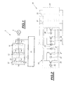
- FIG. 1 represents a three-phase inverter of power 2 intended to supply a rotating electrical machine 4, such as a motor, under the control of an electronic computer 6.
- the engine 4 is, for example, one of the traction motors of a train.
- the computer 6 and the control methods of a three-phase inverter are known. They will not be described in detail here.
- the electrical diagram of the inverter 2 is conventional. It consists of three identical electrical phases, 10, 12 and 14 formed each of two identical power switches 16 and 18. Each power switch is here intended to switch currents of several thousand amperes and able to withstand differences potential of several thousand volts.
- each switch is formed from several electrical switches connected in parallel.
- Fig. 2 shows, for example, a switch formed of four identical switches 20 to 23. Only switch 20 is shown in detail.
- each switch consists of four IGBT transistors 26 to 29, connected in parallel and two diodes 32, 33, connected in antiparallel position across these transistors.
- Each transistor is, for example, capable of withstanding a voltage of 3,000 volts and a maximum rated current of 150 amperes.
- the fact of connecting in parallel the transistors thus makes it possible to produce a switch capable of switching a much larger current than that supported by each of the transistors that constitute it.
- each of the transistors 26 to 29 is connected through a respective resistor 36 to 39 to a not shown gate control electrode.
- FIG. 3 represents in a perspective view the exploded structure of the switch 20.
- the switch comprises a substrate or lower wall 50, formed in an electrically insulating and thermally conductive material, such as a dielectric material.
- the substrate 50 is substantially rectangular and disposed horizontally.
- Each transistor has two opposite planar faces.
- the lower face of each transistor carries the collector electrodes of the transistor, while the upper face carries the gate and emitter electrodes of this same transistor.
- the collector of each of the transistors 26 to 29 and the cathode of the diodes 32 and 33 are soldered to the tracks 52.
- the soldering allows, in addition to the electrical connection to ensure the thermal connection of the collector of the transistors to the substrate 50. a good heat transfer between the collector of each transistor and the substrate 50, the brazing surface is chosen as large as possible.
- Switch 20 also includes a rectangular upper wall or wall 60 formed of an electrically insulative and thermally conductive material. On the inner face of this substrate 60 facing the substrate 50, are also etched electrical tracks 62, 64.
- the track 62 is intended to connect the gates of the transistors 26 to 29 to a gate electrode 66 via the resistors 36 to 39.
- the track 64 is intended to connect the emitters of the transistors 26 to 29 to emitter electrodes 68.
- the gate and emitter electrodes 66, 68 are fixed on the substrate 50.
- the switch 20 also includes a temperature sensor 70 and a heater 72.
- the temperature sensor 70 is fixed on the inner surface of the substrate 50.
- the radiator 72 is a copper radiator having a multitude of fins 74 parallel to each other.
- the space between two consecutive fins 74 forms a small fine channel of substantially rectangular cross section, having, for example, a depth of 3 millimeters and a width of 1 millimeter.
- the radiator 72 is brazed to the outer surface of the substrate 50, so that the fins 74 are parallel to the short side of the substrate 50.
- the substrate 60 is fixed parallel to the substrate 50 and above it by means of a solder roll welding process, known as the "Bumps" welding process .
- welding cylinders 80 are arranged on the different surfaces to be electrically and thermally connected to the tracks 62 and 64 of the substrate 60.
- these cylinders 80 are arranged in particular on the anode surface of the diodes 32 and 33, and on the surfaces of the emitters and gates of the transistors 26 to 29.
- Other cylinders 80 are also arranged to connect the gate 66 and emitter electrodes 68 to the tracks 62 and 64.
- these cylinders 80 are melted so as to electrically, thermally and mechanically connect the substrate 60 to the substrate 50. Moreover, by virtue of the use of these rolls 80, the surface of the contact between the tracks 62, 64 and the corresponding surfaces of the emitters and gates of the transistors is important and also ensures good heat transfer between these brazed surfaces.
- radiator 72 Only a radiator 72 is fixed on the collector side of the transistors because it has been found that the amount of heat that can be discharged by the substrate to which the collectors are brazed is significantly greater than that likely to be discharged by the substrate to which are connected transmitters and grids.
- the space between these two substrates is filled with a dielectric gel so as to isolate the electrical components from the external environment.
- FIGS 4 and 5 show schematically the structure of the switch 18.
- the latter comprises a lower support 90 of electrically insulating material such as plastic arranged horizontally.
- This support 90 is, for example, formed of a horizontal parallelepipedic plate 92 supported by four vertical angles feet 94.
- this plate 92 On the upper surface of this plate 92 is formed an open channel 96 of rectangular section and extending parallel to the longer side of the plate 92.
- This channel 96 is intended to receive a cooling liquid and the radiators 72 of the switches.
- the width and the depth of the channel are adapted to the width and the height of the radiator 72.
- the depth is chosen so that the lower free end of each fin 74 is in contact with the radiator. bottom of the channel 96 so as to define between each fin 74 a mini-channel circulation of the coolant. Such a configuration improves the efficiency of the fins 74.
- the four switches 20 to 23 forming the switch 18 are nested in the support 90, so that their respective radiators 72 are housed in the channel 96.
- the switches 20 to 23 are arranged in such a way that the fins 74 radiators are parallel to the longer side of the support 90. This configuration facilitates the flow of coolant in the channel 96.
- the substrates 50 of the switches 20 to 23 are aligned one behind the other in a same plane parallel to the upper surface of the plate 92.
- the lower surface of the substrates 50 is, for example, fixed by sealing bonding to the edges of the channel 96.
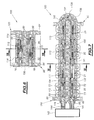
- FIGS 6 and 7 schematically show the structure of an assembled switching module 100.
- This switching module 100 combines, for example, the switches 16 and 18 placed in mirror one above the other.
- the structure of the switch 16 is, for example, identical to that of the switch 18 described with reference to FIGS. 4 and 5.
- the switch 16 comprises four switches 110 to 113 respectively identical to the switches 20 to 23 fixed on a support 120, identical to the support 90.
- the same references as those used to describe the switch 20 are used to designate the identical elements of the switches 110 to 113.
- the open channel in which the switches 110 to 113 are housed carries here reference 116.
- the substrates 60 and switches 16 and 18 respectively face each other.
- a wedge 130 in the form of a horizontal parallelepiped, is housed between the substrates 60 and switches 16 and 18, respectively, so as to maintain the switches 110 to 113 at a predetermined distance from the switches 20 to 23.
- This shim 130 comprises a housing for each of the switches 20 to 23 and 110 to 113.
- the shape of this shim 130 is adapted to seal hermetically the open surface of the channels 116 and 96.
- a single first circuit 132 for circulating a coolant for cooling all the transistors of the module 100 via the substrates 60.
- two horizontal rectilinear recesses 133 and 134 of rectangular cross section extend inside the shim 130 parallel to the longer side of this wedge, and along the outer surface of each of the substrates 60.
- the left end of these recesses 133 and 134 is open while the straight ends of these same recesses are fluidly connected through a first semi-circular recess 136.
- the thickness of the recesses 133 and 134 is less than or equal to one millimeter so as to maximize the efficiency of the heat transfer with respect to the volume of cooling liquid used.
- the shim 130 also has at its right end a second semicircular recess 138 fluidly connecting the right-hand ends of the channels 96 and 116.
- a second circuit 140 for circulating the cooling liquid able to cool all the transistors of the module 100 by intermediate of the substrates 50 is created.
- the circuits 132 and 140 each have a longitudinal section in the form of "U".
- the right end of the shim 130 containing the recesses 136 and 138 is either integral with the shim 130 or, for example, integral with one of the supports 90 or 120.
- the first and second circuits 132 and 140 are fluidly independent of one another.
- the left-hand ends of the channel 96 and the recess 133 are fluidly connected via a Y-shaped connector 141 to the outlet of the same pump 142.
- the left-hand ends of the channel 116 and the recess 134 are fluidly connected by a Y-shaped connector 144 to the inlet of the same pump 142.
- a single pump makes it possible to circulate the liquid of cooling in both circuits 132 and 140.
- the output of the pump 142 is able to propel the coolant inside the circuits 132 and 140, and the pump inlet 142 is able to suck up the coolant present in the circuits 132 and 140.
- each transistor produces heat because of switching losses but also because of the conduction of electricity.
- the largest part of the heat produced is transferred via the collector and the substrate 50 to the radiator 72.
- the presence of small thin channels formed by the spaces between the fins 74 of the radiator 72 makes it possible to increase the contact surface with the coolant circulating in the circuit 140. The heat transfer between the radiator 72 and the coolant is therefore more effectively.
- the other part of the heat produced by the transistors is transferred via the substrates 60, directly to the coolant circulating in the circuit 132.
- the transistors are cooled through their lower and upper faces, the heating of each transistor is considerably limited. It is therefore possible to use these transistors to switch currents much higher than the nominal value of the current for which they are provided. It is therefore possible thanks to the presence of two cooling circuits, respectively the lower and upper faces of the transistors or to fabricate a switching module 100, capable of switching much larger currents of currents with the same number of transistors to reduce the number of transistors and therefore the size of the module 100 to switch an identical current.
- the coolant used is, for example, water.
- other coolants may be used.
- circuits 132 and 140 are also possible to make the circuits 132 and 140 completely independent, that is to say to have no fluid connections 141 and 144 at the left-hand ends of the channels 96 and 116 and recesses 133 and 134. if such an embodiment has a priori no particular advantages, it is nevertheless possible to circulate through the pump 142 a coolant in the circuit 140, and to circulate through another pump an inert cooling gas in the circuit 132.
- the module 100 described comprises a single first circuit 132 for cooling the substrates 60 and a single second cooling circuit of the substrates 50 fed from the same pump.
- the power module comprises a plurality of first cooling circuits for the substrates 60 and a plurality of second cooling circuits for the substrates 50.
- the channels 96 and 116 and the recesses 133 and 134 open to each from their right and left ends. The left open ends are connected in a manner similar to that described with reference to FIG.
- the channels 96 and 116 form two first circuits independent of each other, of circulation of a fluid for cooling the substrates 50, respectively of the switches 16 and 18.
- the recesses 133 and 134 form two second independent circuits of circulation of a fluid for cooling the substrates 60, respectively of the switches 16 and 18.
- the module 100 has been described in the particular case where the transistors are IGBT transistors. However, alternatively, the transistors are, for example, bi-polar transistors or MOSFET transistors or alternatively replaced by other electronic components that it is necessary to cool effectively.
- a power switch may be formed of more than four switches or fewer than four switches, such as, for example, a single switch.
Landscapes
- Engineering & Computer Science (AREA)
- Microelectronics & Electronic Packaging (AREA)
- Power Engineering (AREA)
- Physics & Mathematics (AREA)
- Thermal Sciences (AREA)
- Inverter Devices (AREA)
- Cooling Or The Like Of Electrical Apparatus (AREA)
- Cooling Or The Like Of Semiconductors Or Solid State Devices (AREA)
- Power Conversion In General (AREA)
- Control Of Electric Motors In General (AREA)
Claims (17)
- Leistungsschaltermodul, das Folgendes aufweist:- mindestens einen Leistungsschalter (110 bis 113) über mindestens einem weiteren Leistungsschalter (20 bis 23), wobei jeder Leistungsschalter eine obere und eine untere Wand aufweist, die jeweils durch Wärmeleitung mit einem Kühlfluid gekühlt werden können,- zwei Träger (90) und (120), an denen die unteren beziehungsweise oberen Wände (50) der unteren und oberen Schalter befestigt werden,- untere (96) und obere (116) geschlossene Kanäle, die in den Trägern (90) beziehungsweise (120) vorgesehen und so angeordnet sind, dass sie ein Kühlfluid an den unteren beziehungsweise oberen Wänden (50) der unteren und oberen Schalter entlang zirkulieren lassen,dadurch gekennzeichnet, dass es einen Block (130) zwischen dem oder den oberen Schaltern (110 bis 113) und dem oder den unteren Schaltern (20 bis 23) aufweist, sodass diese in einem vorher festgelegten Abstand voneinander gehalten werden,
und weiter eine untere Aussparung (133) entlang und über der oberen Wand (60) des oder jedes unteren Schalters sowie eine obere Aussparung (134) entlang und unter der unteren Wand (60) des oder jedes oberen Schalters, um die Wände (60) durch Zirkulation eines Kühlfluids in jeder unteren Aussparung (133) und oberen Aussparung (134) zu kühlen. - Modul nach Anspruch 1, bei dem die untere Aussparung (133) und die obere Aussparung (134) zwei miteinander verbundene Enden aufweisen, um einen einzigen Umlaufkreis (132) für das Kühlfluid zu bilden.
- Modul nach Anspruch 1 oder 2, bei dem der oder jeder Schalter (20 bis 23, 110 bis 113) einen einzigen Kühler (72) aufweist, der wärmetechnisch mit der unteren oder oberen Wand verbunden ist, wobei der Kühler mit Rippen (74) versehen ist, die in direktem Kontakt mit dem Kühlfluid in den Kanälen (96, 116) oder den Aussparungen (133, 134) stehen.
- Modul nach Anspruch 3, bei dem nur die obere Wand (50) des oder jedes oberen Schalters (110 bis 113) einen Kühler (72) aufweist und nur die untere Wand des oder jedes unteren Schalters (20 bis 23) einen Kühler (72) aufweist.
- Modul nach Anspruch 3 oder 4, bei dem die Rippen (74) der Kühleren parallel zur Hauptumlaufrichtung des Kühlfluids verlaufen.
- Modul nach einem der vorhergehenden Ansprüche, bei dem der untere Kanal (96) und der obere Kanal (116) miteinander verbunden sind, um einen einzigen Umlaufkreis (140) für das Kühlfluid entlang der oberen Wand (50) des oder jedes oberen Schalters und entlang der unteren Wand (50) des oder jedes unteren Schalters zu bilden.
- Modul nach Anspruch 2 oder 6, bei dem der oder jeder Umlaufkreis (132, 140) für das Kühlfluid mit einer gleichen Pumpe (142) verbunden ist, die das Kühlfluid in dem oder in jedem Umlaufkreis in Umlauf bringt.
- Modul nach einem der vorhergehenden Ansprüche, bei dem mindestens die Enden einer Aussparung und eines Kanals mit einer gemeinsamen Einlass- oder Auslassöffnung (141, 144) für ein gleiches Kühlfluid verbunden sind.
- Modul nach einem der vorhergehenden Ansprüche, bei dem das Kühlfluid eine Flüssigkeit wie beispielsweise Wasser ist.
- Modul nach einem der vorhergehenden Ansprüche, bei dem jeder Schalter Folgendes aufweist:- mehrere Transistoren (26 bis 29) und- elektrische Bahnen (62, 64), an die der Emitter und/oder das Gate jedes Transistors angelötet ist, wobei die Bahnen an einer Innenfläche der Wand (60) ausgebildet sind, die von dem in der Aussparung (133, 134) zirkulierenden Kühlfluid gekühlt wird.
- Modul nach Anspruch 10, bei dem jeder Schalter außerdem elektrische Bahnen (52) aufweist, an die der Kollektor jedes Transistors (26 bis 29) angelötet ist, wobei die Bahnen an einer Innenfläche der Wand ausgebildet sind, die von dem in einem Kanal (96, 116) zirkulierenden Kühlfluid gekühlt wird.
- Modul nach Anspruch 10 oder 11, bei dem die Transistoren elektrisch über geschmolzene Lotzylinder (80) mit den elektrischen Bahnen verbunden sind.
- Modul nach einem der vorhergehenden Ansprüche, bei dem der Block (130) im Wesentlichen parallelepipedförmig ist und eine Aufnahme für jeden Schalter (110 bis 113) und (20 bis 23) besitzt.
- Modul nach Anspruch 13, bei dem die Form des Blocks (130) geeignet ist, die offene Fläche der unteren Kanäle (96) und der oberen Kanäle (116) hermetisch zu verschließen.
- Modul nach Anspruch 2 und Anspruch 13 oder 14, bei dem der einzige Umlaufkreis (132) für Kühlfluid innerhalb des Blocks (130) vorgesehen ist und bei dem die untere Aussparung (133) und die obere Aussparung (134) einen rechteckigen Querschnitt aufweisen und sich innerhalb des Blocks parallel zu seiner größten Seite erstrecken.
- Modul nach einem der vorhergehenden Ansprüche, bei dem die Dicke der unteren Aussparung (133) und der oberen Aussparung (134) kleiner oder gleich einem Millimeter ist.
- Mehrphasen-Wechselrichter, bei dem jede Phase zwei Trennschalter (16, 18) aufweist, die jeweils aus mindestens einem Schalter (20 bis 23, 110 bis 113) gebildet sind, dadurch gekennzeichnet, dass die beiden Trennschalter (16, 18) einer gleichen Phase mithilfe eines einzigen Leistungsschaltermoduls nach einem der vorhergehenden Ansprüche hergestellt werden.
Applications Claiming Priority (2)
| Application Number | Priority Date | Filing Date | Title |
|---|---|---|---|
| FR0304407A FR2853808B1 (fr) | 2003-04-09 | 2003-04-09 | Module de commutation de puissance et ondulateur equipe de ce module |
| FR0304407 | 2003-04-09 |
Publications (2)
| Publication Number | Publication Date |
|---|---|
| EP1467607A1 EP1467607A1 (de) | 2004-10-13 |
| EP1467607B1 true EP1467607B1 (de) | 2007-08-22 |
Family
ID=32865405
Family Applications (1)
| Application Number | Title | Priority Date | Filing Date |
|---|---|---|---|
| EP04101448A Expired - Lifetime EP1467607B1 (de) | 2003-04-09 | 2004-04-07 | Leistungsschaltermodul und Wechselrichter mit einem solchen Modul |
Country Status (7)
| Country | Link |
|---|---|
| US (1) | US7042725B2 (de) |
| EP (1) | EP1467607B1 (de) |
| JP (1) | JP2004312997A (de) |
| AT (1) | ATE371360T1 (de) |
| DE (1) | DE602004008365T2 (de) |
| ES (1) | ES2290622T3 (de) |
| FR (1) | FR2853808B1 (de) |
Cited By (3)
| Publication number | Priority date | Publication date | Assignee | Title |
|---|---|---|---|---|
| US8294258B2 (en) | 2010-04-02 | 2012-10-23 | Hitachi, Ltd. | Power semiconductor module |
| EP3945572A1 (de) | 2020-07-30 | 2022-02-02 | Siemens Aktiengesellschaft | Leistungshalbleitermodul und herstellungsverfahren für ein leistungshalbleitermodul |
| WO2022028957A1 (de) | 2020-08-05 | 2022-02-10 | Siemens Aktiengesellschaft | Leistungshalbleitermodulsystem und herstellungsverfahren für ein leistungshalbleitermodulsystem |
Families Citing this family (41)
| Publication number | Priority date | Publication date | Assignee | Title |
|---|---|---|---|---|
| DE10317580B4 (de) * | 2002-04-18 | 2010-09-16 | Hitachi, Ltd. | Elektrische Wechselrichtervorrichtung mit einem Flüssigkeitskanal sowie Elektrofahrzeug mit einer derartigen Wechselrichtervorrichtung |
| JP3963175B2 (ja) * | 2004-03-19 | 2007-08-22 | 日産自動車株式会社 | 温度検出装置および温度検出用プログラム |
| JP4284625B2 (ja) * | 2005-06-22 | 2009-06-24 | 株式会社デンソー | 三相インバータ装置 |
| US20070165376A1 (en) * | 2006-01-17 | 2007-07-19 | Norbert Bones | Three phase inverter power stage and assembly |
| JP4770490B2 (ja) * | 2006-01-31 | 2011-09-14 | トヨタ自動車株式会社 | パワー半導体素子の冷却構造およびインバータ |
| EP2122682B1 (de) * | 2006-12-21 | 2019-05-08 | ABB Research LTD | Halbleitermodul |
| FI120855B (fi) * | 2007-02-15 | 2010-03-31 | Kone Corp | Laitteisto ja menetelmä moottorin tehonsyötön ohjaamiseksi |
| US7965508B2 (en) * | 2007-03-27 | 2011-06-21 | Denso Corporation | Cooling device for electronic component and power converter equipped with the same |
| JP4683003B2 (ja) * | 2007-03-30 | 2011-05-11 | 株式会社デンソー | パワーモジュール及びこれを用いた電力変換装置 |
| US7977821B2 (en) * | 2007-05-10 | 2011-07-12 | Honeywell International Inc. | High power density switch module with improved thermal management and packaging |
| JP5120604B2 (ja) * | 2007-05-22 | 2013-01-16 | アイシン・エィ・ダブリュ株式会社 | 半導体モジュール及びインバータ装置 |
| DE102008021898B4 (de) * | 2008-05-02 | 2015-10-01 | Siemens Aktiengesellschaft | Detektionseinrichtung mit einer Vorrichtung zur Kühlung |
| DE202009005837U1 (de) * | 2009-04-18 | 2010-09-16 | Brose Fahrzeugteile Gmbh & Co. Kommanditgesellschaft, Hallstadt | Schaltungsanordnung zum Betrieb eines Gleichstrommotors |
| US8064198B2 (en) * | 2009-06-29 | 2011-11-22 | Honda Motor Co., Ltd. | Cooling device for semiconductor element module and magnetic part |
| US8358506B2 (en) * | 2010-08-27 | 2013-01-22 | Direct Grid Technologies, LLC | Mechanical arrangement for use within galvanically-isolated, low-profile micro-inverters for solar power installations |
| US9252069B2 (en) | 2010-08-31 | 2016-02-02 | Teledyne Scientific & Imaging, Llc | High power module cooling system |
| WO2012051704A1 (en) | 2010-10-19 | 2012-04-26 | Electronic Motion Systems Holdings Limited | A power module for converting dc to ac |
| US8804340B2 (en) * | 2011-06-08 | 2014-08-12 | International Rectifier Corporation | Power semiconductor package with double-sided cooling |
| US9640617B2 (en) | 2011-09-11 | 2017-05-02 | Cree, Inc. | High performance power module |
| US9373617B2 (en) | 2011-09-11 | 2016-06-21 | Cree, Inc. | High current, low switching loss SiC power module |
| WO2013036370A1 (en) | 2011-09-11 | 2013-03-14 | Cree, Inc. | High current density power module comprising transistors with improved layout |
| US9261924B2 (en) * | 2013-09-05 | 2016-02-16 | Dell Inc. | Heat pipe assemblies |
| TWI736050B (zh) | 2014-08-20 | 2021-08-11 | 愛爾蘭商納維達斯半導體有限公司 | 具有分布閘極之功率電晶體 |
| CN104269385B (zh) * | 2014-10-21 | 2017-12-19 | 矽力杰半导体技术(杭州)有限公司 | 封装组件及其制造方法 |
| DE102014227025A1 (de) * | 2014-12-30 | 2016-06-30 | Robert Bosch Gmbh | Parametrierbares Leistungsbauteil und Verfahren zu dessen Betrieb |
| WO2016203885A1 (ja) * | 2015-06-17 | 2016-12-22 | 富士電機株式会社 | パワー半導体モジュール及び冷却器 |
| CN108028242B (zh) * | 2015-09-30 | 2021-08-17 | 敏捷电源开关三维集成Apsi3D | 包括附加迹线的半导体功率器件及制造半导体功率器件的方法 |
| US9781867B2 (en) * | 2016-02-19 | 2017-10-03 | Ford Global Technologies, Llc | Power module assembly for a vehicle power inverter |
| FR3049159B1 (fr) * | 2016-03-15 | 2019-10-25 | Institut Vedecom | Module d’electronique de puissance refroidi, moteur et vehicule integrant un tel module |
| US20170336152A1 (en) * | 2016-05-20 | 2017-11-23 | Hyundai Motor Company | Double-sided cooler for cooling both sides of electronic component |
| US11022383B2 (en) | 2016-06-16 | 2021-06-01 | Teledyne Scientific & Imaging, Llc | Interface-free thermal management system for high power devices co-fabricated with electronic circuit |
| WO2018146816A1 (ja) * | 2017-02-13 | 2018-08-16 | 新電元工業株式会社 | 電子機器 |
| US11368031B2 (en) | 2017-11-08 | 2022-06-21 | Eaton Intelligent Power Limited | Power distribution and circuit protection for a mobile application having a high efficiency inverter |
| US11070049B2 (en) | 2017-11-08 | 2021-07-20 | Eaton Intelligent Power Limited | System, method, and apparatus for power distribution in an electric mobile application using a combined breaker and relay |
| US11108225B2 (en) | 2017-11-08 | 2021-08-31 | Eaton Intelligent Power Limited | System, method, and apparatus for power distribution in an electric mobile application using a combined breaker and relay |
| US11052784B2 (en) | 2017-11-08 | 2021-07-06 | Eaton Intelligent Power Limited | Power distribution unit and fuse management for an electric mobile application |
| WO2019197459A2 (en) * | 2018-04-10 | 2019-10-17 | Eaton Intelligent Power Limited | System, method, and apparatus for power distribution in an electric mobile application using a combined breaker and relay |
| US11689010B2 (en) | 2019-02-22 | 2023-06-27 | Eaton Intelligent Power Limited | Coolant fitting promoting turbulent flow |
| WO2021009217A2 (en) | 2019-07-15 | 2021-01-21 | Eaton Intelligent Power Limited | Power distribution and circuit protection for a mobile application having a high efficiency inverter |
| CN113632364B (zh) * | 2019-11-22 | 2023-08-08 | 东芝三菱电机产业系统株式会社 | 电力变换单元 |
| CN111585452A (zh) * | 2020-04-24 | 2020-08-25 | 中国南方电网有限责任公司超高压输电公司广州局 | 一种新型换流阀用均压电极及其安装组件、安装方法 |
Family Cites Families (11)
| Publication number | Priority date | Publication date | Assignee | Title |
|---|---|---|---|---|
| BE794291A (fr) * | 1972-01-22 | 1973-05-16 | Siemens Ag | Dispositif a semi-conducteurs regroupant plusieurs corps semi-conducteurs en forme de pastille |
| US3921201A (en) * | 1972-01-22 | 1975-11-18 | Siemens Ag | Improved liquid cooled semiconductor disk arrangement |
| US4884168A (en) * | 1988-12-14 | 1989-11-28 | Cray Research, Inc. | Cooling plate with interboard connector apertures for circuit board assemblies |
| US5003376A (en) * | 1989-03-28 | 1991-03-26 | Coriolis Corporation | Cooling of large high power semi-conductors |
| JP2660879B2 (ja) * | 1992-05-25 | 1997-10-08 | マンネスマン・アクチエンゲゼルシャフト | 半導体スイッチを有する電気機械 |
| US5504378A (en) * | 1994-06-10 | 1996-04-02 | Westinghouse Electric Corp. | Direct cooled switching module for electric vehicle propulsion system |
| FR2765067B1 (fr) * | 1997-06-19 | 1999-07-16 | Alsthom Cge Alcatel | Module d'electronique de puissance et un dispositif d'electronique de puissance pourvu de tels modules |
| DE19735531A1 (de) * | 1997-08-16 | 1999-02-18 | Abb Research Ltd | Leistungshalbleitermodul mit in Submodulen integrierten Kühlern |
| FR2775416B1 (fr) * | 1998-02-23 | 2000-06-23 | Gec Alsthom Transport Sa | Element de refroidissement pour dispositif electronique de puissance et dispositif electronique de puissance comprenant un tel element |
| FR2809281B1 (fr) * | 2000-05-22 | 2002-07-12 | Alstom | Dispositif electronique de puissance |
| US6865080B2 (en) * | 2002-01-16 | 2005-03-08 | Rockwell Automation Technologies, Inc. | Compact fluid cooled power converter supporting multiple circuit boards |
-
2003
- 2003-04-09 FR FR0304407A patent/FR2853808B1/fr not_active Expired - Fee Related
-
2004
- 2004-04-06 JP JP2004111904A patent/JP2004312997A/ja active Pending
- 2004-04-07 ES ES04101448T patent/ES2290622T3/es not_active Expired - Lifetime
- 2004-04-07 EP EP04101448A patent/EP1467607B1/de not_active Expired - Lifetime
- 2004-04-07 AT AT04101448T patent/ATE371360T1/de active
- 2004-04-07 DE DE602004008365T patent/DE602004008365T2/de not_active Expired - Lifetime
- 2004-04-08 US US10/821,031 patent/US7042725B2/en not_active Expired - Lifetime
Non-Patent Citations (1)
| Title |
|---|
| None * |
Cited By (4)
| Publication number | Priority date | Publication date | Assignee | Title |
|---|---|---|---|---|
| US8294258B2 (en) | 2010-04-02 | 2012-10-23 | Hitachi, Ltd. | Power semiconductor module |
| EP3945572A1 (de) | 2020-07-30 | 2022-02-02 | Siemens Aktiengesellschaft | Leistungshalbleitermodul und herstellungsverfahren für ein leistungshalbleitermodul |
| WO2022023326A1 (de) | 2020-07-30 | 2022-02-03 | Siemens Aktiengesellschaft | Leistungshalbleitermodul und herstellungsverfahren für ein leistungshalbleitermodul |
| WO2022028957A1 (de) | 2020-08-05 | 2022-02-10 | Siemens Aktiengesellschaft | Leistungshalbleitermodulsystem und herstellungsverfahren für ein leistungshalbleitermodulsystem |
Also Published As
| Publication number | Publication date |
|---|---|
| FR2853808B1 (fr) | 2006-09-15 |
| FR2853808A1 (fr) | 2004-10-15 |
| JP2004312997A (ja) | 2004-11-04 |
| ATE371360T1 (de) | 2007-09-15 |
| EP1467607A1 (de) | 2004-10-13 |
| US20040207968A1 (en) | 2004-10-21 |
| DE602004008365D1 (de) | 2007-10-04 |
| ES2290622T3 (es) | 2008-02-16 |
| US7042725B2 (en) | 2006-05-09 |
| DE602004008365T2 (de) | 2008-05-15 |
Similar Documents
| Publication | Publication Date | Title |
|---|---|---|
| EP1467607A1 (de) | Leistungsschaltermodul und Wechselrichter mit einem solchen Modul | |
| EP1158656B1 (de) | Elektronische Leistungsvorrichtung | |
| US6101206A (en) | Laser-diode device including heat-conducting walls, semiconductor strips and isolating seals and process for making laser-diode device | |
| FR2813440A1 (fr) | Dispositif a semiconducteur pour la commande d'energie electrique | |
| CN111883523A (zh) | 半导体构件、机动车和用于制造半导体构件的方法 | |
| FR2824180A1 (fr) | Module de condensateur et dispositif semi-conducteur utilisant le module de condensateur | |
| FR3065319A1 (fr) | Module electronique de puissance et convertisseur electrique de puissance l’incorporant | |
| FR3014249A1 (fr) | Module de batterie pour vehicule electrique ou hybride integrant un echangeur de chaleur en contact avec les bornes du module | |
| FR2879021A1 (fr) | Dispositif a semiconducteur de puissance | |
| FR2951019A1 (fr) | Module de puissance pour vehicule automobile | |
| WO2014095610A1 (fr) | Dispositif de refroidissement pour carte de circuit imprime | |
| FR2500215A1 (fr) | Dispositif de refroidissement d'un composant electronique de puissance, et composant encapsule dans un boitier muni d'un tel dispositif | |
| FR3049159B1 (fr) | Module d’electronique de puissance refroidi, moteur et vehicule integrant un tel module | |
| EP0734066B1 (de) | Elektronischer Leistungsmodul | |
| FR3106239A1 (fr) | Bloc-batterie équipé de moyens passifs de dissipation thermique | |
| EP1484797A1 (de) | Leistungswechselrichter und dessen Herstellung | |
| FR3113439A1 (fr) | Dispositif électrique à refroidissement par boîte à eau et procédé de fabrication d’un tel dispositif | |
| EP1032114B1 (de) | Elektrisches Modul für Fahrzeug-, insbesondere Autolichtmaschine, und ein solches Modul und eine solche Lichtmaschine beinhaltende Anordnung | |
| FR2847762A1 (fr) | Element de module electronique de puissance | |
| EP0016670B1 (de) | Thermoelektrische Anlage | |
| FR3110034A1 (fr) | Module electrique avec surmoulage et systemes comprenant un tel module electrique | |
| FR3143234A1 (fr) | Carter d’onduleur comportant des plots de refroidissement et onduleur comportant un tel capteur | |
| FR3113440A1 (fr) | Dispositif électrique à refroidissement par boîte à eau et système électrique comportant un tel dispositif | |
| FR3156594A1 (fr) | Ensemble comprenant un élément électrochimique et une pompe électrohydrodynamique, module de batterie, batterie et procédé associés | |
| WO2023118111A1 (fr) | Module de puissance avec surmoulage et systeme electrique comprenant un tel module de puissance |
Legal Events
| Date | Code | Title | Description |
|---|---|---|---|
| PUAI | Public reference made under article 153(3) epc to a published international application that has entered the european phase |
Free format text: ORIGINAL CODE: 0009012 |
|
| AK | Designated contracting states |
Kind code of ref document: A1 Designated state(s): AT BE BG CH CY CZ DE DK EE ES FI FR GB GR HU IE IT LI LU MC NL PL PT RO SE SI SK TR |
|
| AX | Request for extension of the european patent |
Extension state: AL HR LT LV MK |
|
| RAP1 | Party data changed (applicant data changed or rights of an application transferred) |
Owner name: ALSTOM |
|
| 17P | Request for examination filed |
Effective date: 20050413 |
|
| AKX | Designation fees paid |
Designated state(s): AT BE BG CH CY CZ DE DK EE ES FI FR GB GR HU IE IT LI LU MC NL PL PT RO SE SI SK TR |
|
| GRAP | Despatch of communication of intention to grant a patent |
Free format text: ORIGINAL CODE: EPIDOSNIGR1 |
|
| GRAS | Grant fee paid |
Free format text: ORIGINAL CODE: EPIDOSNIGR3 |
|
| GRAA | (expected) grant |
Free format text: ORIGINAL CODE: 0009210 |
|
| AK | Designated contracting states |
Kind code of ref document: B1 Designated state(s): AT BE BG CH CY CZ DE DK EE ES FI FR GB GR HU IE IT LI LU MC NL PL PT RO SE SI SK TR |
|
| REG | Reference to a national code |
Ref country code: GB Ref legal event code: FG4D Free format text: NOT ENGLISH |
|
| REG | Reference to a national code |
Ref country code: CH Ref legal event code: EP |
|
| REG | Reference to a national code |
Ref country code: IE Ref legal event code: FG4D Free format text: LANGUAGE OF EP DOCUMENT: FRENCH |
|
| REF | Corresponds to: |
Ref document number: 602004008365 Country of ref document: DE Date of ref document: 20071004 Kind code of ref document: P |
|
| GBT | Gb: translation of ep patent filed (gb section 77(6)(a)/1977) |
Effective date: 20070926 |
|
| REG | Reference to a national code |
Ref country code: SE Ref legal event code: TRGR |
|
| PG25 | Lapsed in a contracting state [announced via postgrant information from national office to epo] |
Ref country code: BG Free format text: LAPSE BECAUSE OF FAILURE TO SUBMIT A TRANSLATION OF THE DESCRIPTION OR TO PAY THE FEE WITHIN THE PRESCRIBED TIME-LIMIT Effective date: 20071122 Ref country code: FI Free format text: LAPSE BECAUSE OF FAILURE TO SUBMIT A TRANSLATION OF THE DESCRIPTION OR TO PAY THE FEE WITHIN THE PRESCRIBED TIME-LIMIT Effective date: 20070822 |
|
| REG | Reference to a national code |
Ref country code: ES Ref legal event code: FG2A Ref document number: 2290622 Country of ref document: ES Kind code of ref document: T3 |
|
| PG25 | Lapsed in a contracting state [announced via postgrant information from national office to epo] |
Ref country code: PL Free format text: LAPSE BECAUSE OF FAILURE TO SUBMIT A TRANSLATION OF THE DESCRIPTION OR TO PAY THE FEE WITHIN THE PRESCRIBED TIME-LIMIT Effective date: 20070822 |
|
| REG | Reference to a national code |
Ref country code: IE Ref legal event code: FD4D |
|
| PG25 | Lapsed in a contracting state [announced via postgrant information from national office to epo] |
Ref country code: GR Free format text: LAPSE BECAUSE OF FAILURE TO SUBMIT A TRANSLATION OF THE DESCRIPTION OR TO PAY THE FEE WITHIN THE PRESCRIBED TIME-LIMIT Effective date: 20071123 Ref country code: DK Free format text: LAPSE BECAUSE OF FAILURE TO SUBMIT A TRANSLATION OF THE DESCRIPTION OR TO PAY THE FEE WITHIN THE PRESCRIBED TIME-LIMIT Effective date: 20070822 |
|
| PG25 | Lapsed in a contracting state [announced via postgrant information from national office to epo] |
Ref country code: PT Free format text: LAPSE BECAUSE OF FAILURE TO SUBMIT A TRANSLATION OF THE DESCRIPTION OR TO PAY THE FEE WITHIN THE PRESCRIBED TIME-LIMIT Effective date: 20080122 Ref country code: CZ Free format text: LAPSE BECAUSE OF FAILURE TO SUBMIT A TRANSLATION OF THE DESCRIPTION OR TO PAY THE FEE WITHIN THE PRESCRIBED TIME-LIMIT Effective date: 20070822 Ref country code: SK Free format text: LAPSE BECAUSE OF FAILURE TO SUBMIT A TRANSLATION OF THE DESCRIPTION OR TO PAY THE FEE WITHIN THE PRESCRIBED TIME-LIMIT Effective date: 20070822 Ref country code: IE Free format text: LAPSE BECAUSE OF FAILURE TO SUBMIT A TRANSLATION OF THE DESCRIPTION OR TO PAY THE FEE WITHIN THE PRESCRIBED TIME-LIMIT Effective date: 20070822 |
|
| PLBE | No opposition filed within time limit |
Free format text: ORIGINAL CODE: 0009261 |
|
| STAA | Information on the status of an ep patent application or granted ep patent |
Free format text: STATUS: NO OPPOSITION FILED WITHIN TIME LIMIT |
|
| PG25 | Lapsed in a contracting state [announced via postgrant information from national office to epo] |
Ref country code: RO Free format text: LAPSE BECAUSE OF FAILURE TO SUBMIT A TRANSLATION OF THE DESCRIPTION OR TO PAY THE FEE WITHIN THE PRESCRIBED TIME-LIMIT Effective date: 20070822 |
|
| 26N | No opposition filed |
Effective date: 20080526 |
|
| PG25 | Lapsed in a contracting state [announced via postgrant information from national office to epo] |
Ref country code: MC Free format text: LAPSE BECAUSE OF NON-PAYMENT OF DUE FEES Effective date: 20080430 |
|
| PG25 | Lapsed in a contracting state [announced via postgrant information from national office to epo] |
Ref country code: EE Free format text: LAPSE BECAUSE OF FAILURE TO SUBMIT A TRANSLATION OF THE DESCRIPTION OR TO PAY THE FEE WITHIN THE PRESCRIBED TIME-LIMIT Effective date: 20070822 |
|
| PG25 | Lapsed in a contracting state [announced via postgrant information from national office to epo] |
Ref country code: SI Free format text: LAPSE BECAUSE OF FAILURE TO SUBMIT A TRANSLATION OF THE DESCRIPTION OR TO PAY THE FEE WITHIN THE PRESCRIBED TIME-LIMIT Effective date: 20070822 |
|
| PG25 | Lapsed in a contracting state [announced via postgrant information from national office to epo] |
Ref country code: CY Free format text: LAPSE BECAUSE OF FAILURE TO SUBMIT A TRANSLATION OF THE DESCRIPTION OR TO PAY THE FEE WITHIN THE PRESCRIBED TIME-LIMIT Effective date: 20070822 |
|
| REG | Reference to a national code |
Ref country code: FR Ref legal event code: TP |
|
| PG25 | Lapsed in a contracting state [announced via postgrant information from national office to epo] |
Ref country code: LU Free format text: LAPSE BECAUSE OF NON-PAYMENT OF DUE FEES Effective date: 20080407 Ref country code: HU Free format text: LAPSE BECAUSE OF FAILURE TO SUBMIT A TRANSLATION OF THE DESCRIPTION OR TO PAY THE FEE WITHIN THE PRESCRIBED TIME-LIMIT Effective date: 20080223 |
|
| REG | Reference to a national code |
Ref country code: FR Ref legal event code: TP Owner name: ALSTOM TRANSPORT TECHNOLOGIES, FR Effective date: 20141209 |
|
| REG | Reference to a national code |
Ref country code: CH Ref legal event code: PUE Owner name: ALSTOM TRANSPORT SA, FR Free format text: FORMER OWNER: ALSTOM, FR Ref country code: CH Ref legal event code: PUE Owner name: ALSTOM TRANSPORT TECHNOLOGIES, FR Free format text: FORMER OWNER: ALSTOM TRANSPORT SA, FR |
|
| REG | Reference to a national code |
Ref country code: DE Ref legal event code: R082 Ref document number: 602004008365 Country of ref document: DE Representative=s name: TER MEER STEINMEISTER & PARTNER PATENTANWAELTE, DE Ref country code: DE Ref legal event code: R081 Ref document number: 602004008365 Country of ref document: DE Owner name: ALSTOM TRANSPORT TECHNOLOGIES, FR Free format text: FORMER OWNER: ALSTOM, LEVALLOIS-PERRET, FR |
|
| REG | Reference to a national code |
Ref country code: GB Ref legal event code: 732E Free format text: REGISTERED BETWEEN 20151001 AND 20151007 |
|
| REG | Reference to a national code |
Ref country code: GB Ref legal event code: 732E Free format text: REGISTERED BETWEEN 20151119 AND 20151125 |
|
| REG | Reference to a national code |
Ref country code: FR Ref legal event code: PLFP Year of fee payment: 13 |
|
| REG | Reference to a national code |
Ref country code: FR Ref legal event code: PLFP Year of fee payment: 14 |
|
| REG | Reference to a national code |
Ref country code: DE Ref legal event code: R082 Ref document number: 602004008365 Country of ref document: DE Representative=s name: TER MEER STEINMEISTER & PARTNER PATENTANWAELTE, DE Ref country code: DE Ref legal event code: R081 Ref document number: 602004008365 Country of ref document: DE Owner name: ALSTOM TRANSPORT TECHNOLOGIES, FR Free format text: FORMER OWNER: ALSTOM TRANSPORT TECHNOLOGIES, LEVALLOIS-PERRET, FR |
|
| REG | Reference to a national code |
Ref country code: ES Ref legal event code: PC2A Owner name: ALSTOM TRANSPORT SA Effective date: 20170928 |
|
| REG | Reference to a national code |
Ref country code: CH Ref legal event code: NV Representative=s name: BUGNION S.A., CH Ref country code: CH Ref legal event code: PCOW Free format text: NEW ADDRESS: 48 RUE ALBERT DHALENNE, 93400 SAINT-OUEN (FR) |
|
| REG | Reference to a national code |
Ref country code: FR Ref legal event code: CA Effective date: 20180103 |
|
| REG | Reference to a national code |
Ref country code: AT Ref legal event code: PC Ref document number: 371360 Country of ref document: AT Kind code of ref document: T Owner name: ALSTOM TRANSPORT TECHNOLOGIES, FR Effective date: 20180220 |
|
| REG | Reference to a national code |
Ref country code: FR Ref legal event code: PLFP Year of fee payment: 15 |
|
| PGFP | Annual fee paid to national office [announced via postgrant information from national office to epo] |
Ref country code: CH Payment date: 20200420 Year of fee payment: 17 Ref country code: FR Payment date: 20200420 Year of fee payment: 17 Ref country code: DE Payment date: 20200420 Year of fee payment: 17 Ref country code: ES Payment date: 20200629 Year of fee payment: 17 Ref country code: NL Payment date: 20200427 Year of fee payment: 17 |
|
| PGFP | Annual fee paid to national office [announced via postgrant information from national office to epo] |
Ref country code: SE Payment date: 20200427 Year of fee payment: 17 Ref country code: BE Payment date: 20200427 Year of fee payment: 17 Ref country code: GB Payment date: 20200427 Year of fee payment: 17 Ref country code: IT Payment date: 20200428 Year of fee payment: 17 |
|
| PGFP | Annual fee paid to national office [announced via postgrant information from national office to epo] |
Ref country code: AT Payment date: 20200421 Year of fee payment: 17 |
|
| REG | Reference to a national code |
Ref country code: ES Ref legal event code: PC2A Owner name: ALSTOM TRANSPORT TECHNOLOGIES Effective date: 20210528 |
|
| PGFP | Annual fee paid to national office [announced via postgrant information from national office to epo] |
Ref country code: TR Payment date: 20210401 Year of fee payment: 18 |
|
| REG | Reference to a national code |
Ref country code: DE Ref legal event code: R119 Ref document number: 602004008365 Country of ref document: DE |
|
| REG | Reference to a national code |
Ref country code: SE Ref legal event code: EUG |
|
| REG | Reference to a national code |
Ref country code: NL Ref legal event code: MM Effective date: 20210501 |
|
| REG | Reference to a national code |
Ref country code: AT Ref legal event code: MM01 Ref document number: 371360 Country of ref document: AT Kind code of ref document: T Effective date: 20210407 |
|
| GBPC | Gb: european patent ceased through non-payment of renewal fee |
Effective date: 20210407 |
|
| REG | Reference to a national code |
Ref country code: BE Ref legal event code: MM Effective date: 20210430 |
|
| PG25 | Lapsed in a contracting state [announced via postgrant information from national office to epo] |
Ref country code: SE Free format text: LAPSE BECAUSE OF NON-PAYMENT OF DUE FEES Effective date: 20210408 Ref country code: FR Free format text: LAPSE BECAUSE OF NON-PAYMENT OF DUE FEES Effective date: 20210430 Ref country code: GB Free format text: LAPSE BECAUSE OF NON-PAYMENT OF DUE FEES Effective date: 20210407 Ref country code: DE Free format text: LAPSE BECAUSE OF NON-PAYMENT OF DUE FEES Effective date: 20211103 Ref country code: LI Free format text: LAPSE BECAUSE OF NON-PAYMENT OF DUE FEES Effective date: 20210430 Ref country code: AT Free format text: LAPSE BECAUSE OF NON-PAYMENT OF DUE FEES Effective date: 20210407 Ref country code: CH Free format text: LAPSE BECAUSE OF NON-PAYMENT OF DUE FEES Effective date: 20210430 |
|
| PG25 | Lapsed in a contracting state [announced via postgrant information from national office to epo] |
Ref country code: NL Free format text: LAPSE BECAUSE OF NON-PAYMENT OF DUE FEES Effective date: 20210501 |
|
| REG | Reference to a national code |
Ref country code: ES Ref legal event code: FD2A Effective date: 20220630 |
|
| PG25 | Lapsed in a contracting state [announced via postgrant information from national office to epo] |
Ref country code: ES Free format text: LAPSE BECAUSE OF NON-PAYMENT OF DUE FEES Effective date: 20210408 Ref country code: BE Free format text: LAPSE BECAUSE OF NON-PAYMENT OF DUE FEES Effective date: 20210430 |
|
| PG25 | Lapsed in a contracting state [announced via postgrant information from national office to epo] |
Ref country code: IT Free format text: LAPSE BECAUSE OF NON-PAYMENT OF DUE FEES Effective date: 20200407 |
|
| PG25 | Lapsed in a contracting state [announced via postgrant information from national office to epo] |
Ref country code: TR Free format text: LAPSE BECAUSE OF NON-PAYMENT OF DUE FEES Effective date: 20220407 |
|
| PG25 | Lapsed in a contracting state [announced via postgrant information from national office to epo] |
Ref country code: IT Free format text: LAPSE BECAUSE OF NON-PAYMENT OF DUE FEES Effective date: 20210407 |