EP1469355A1 - Méthode de fabrication d'un dispositif - Google Patents
Méthode de fabrication d'un dispositif Download PDFInfo
- Publication number
- EP1469355A1 EP1469355A1 EP03258052A EP03258052A EP1469355A1 EP 1469355 A1 EP1469355 A1 EP 1469355A1 EP 03258052 A EP03258052 A EP 03258052A EP 03258052 A EP03258052 A EP 03258052A EP 1469355 A1 EP1469355 A1 EP 1469355A1
- Authority
- EP
- European Patent Office
- Prior art keywords
- substrate
- alignment
- markers
- alignment marker
- marker
- Prior art date
- Legal status (The legal status is an assumption and is not a legal conclusion. Google has not performed a legal analysis and makes no representation as to the accuracy of the status listed.)
- Granted
Links
- 238000004519 manufacturing process Methods 0.000 title claims abstract description 10
- 239000000758 substrate Substances 0.000 claims abstract description 71
- 239000003550 marker Substances 0.000 claims description 20
- 238000000034 method Methods 0.000 claims description 20
- 238000000059 patterning Methods 0.000 claims description 14
- 230000015572 biosynthetic process Effects 0.000 claims description 2
- 238000005530 etching Methods 0.000 claims description 2
- 230000005855 radiation Effects 0.000 description 19
- 239000010410 layer Substances 0.000 description 9
- 230000003287 optical effect Effects 0.000 description 6
- 238000009826 distribution Methods 0.000 description 3
- 238000007654 immersion Methods 0.000 description 3
- XUIMIQQOPSSXEZ-UHFFFAOYSA-N Silicon Chemical compound [Si] XUIMIQQOPSSXEZ-UHFFFAOYSA-N 0.000 description 2
- 238000005286 illumination Methods 0.000 description 2
- 238000003384 imaging method Methods 0.000 description 2
- 239000007788 liquid Substances 0.000 description 2
- 238000001459 lithography Methods 0.000 description 2
- 230000010363 phase shift Effects 0.000 description 2
- 229910052710 silicon Inorganic materials 0.000 description 2
- 239000010703 silicon Substances 0.000 description 2
- 230000003068 static effect Effects 0.000 description 2
- 239000000853 adhesive Substances 0.000 description 1
- 230000001070 adhesive effect Effects 0.000 description 1
- 238000003491 array Methods 0.000 description 1
- 230000002238 attenuated effect Effects 0.000 description 1
- 230000001143 conditioned effect Effects 0.000 description 1
- 238000001514 detection method Methods 0.000 description 1
- 230000009977 dual effect Effects 0.000 description 1
- 230000005670 electromagnetic radiation Effects 0.000 description 1
- 238000010894 electron beam technology Methods 0.000 description 1
- 239000012530 fluid Substances 0.000 description 1
- 238000007689 inspection Methods 0.000 description 1
- 238000010884 ion-beam technique Methods 0.000 description 1
- 239000002346 layers by function Substances 0.000 description 1
- 239000004973 liquid crystal related substance Substances 0.000 description 1
- 230000005381 magnetic domain Effects 0.000 description 1
- 239000000463 material Substances 0.000 description 1
- 239000011159 matrix material Substances 0.000 description 1
- 230000015654 memory Effects 0.000 description 1
- QSHDDOUJBYECFT-UHFFFAOYSA-N mercury Chemical compound [Hg] QSHDDOUJBYECFT-UHFFFAOYSA-N 0.000 description 1
- 229910052753 mercury Inorganic materials 0.000 description 1
- 239000002245 particle Substances 0.000 description 1
- 239000011295 pitch Substances 0.000 description 1
- 210000001747 pupil Anatomy 0.000 description 1
- 238000007493 shaping process Methods 0.000 description 1
- 239000010409 thin film Substances 0.000 description 1
- XLYOFNOQVPJJNP-UHFFFAOYSA-N water Substances O XLYOFNOQVPJJNP-UHFFFAOYSA-N 0.000 description 1
Images


Classifications
-
- G—PHYSICS
- G03—PHOTOGRAPHY; CINEMATOGRAPHY; ANALOGOUS TECHNIQUES USING WAVES OTHER THAN OPTICAL WAVES; ELECTROGRAPHY; HOLOGRAPHY
- G03F—PHOTOMECHANICAL PRODUCTION OF TEXTURED OR PATTERNED SURFACES, e.g. FOR PRINTING, FOR PROCESSING OF SEMICONDUCTOR DEVICES; MATERIALS THEREFOR; ORIGINALS THEREFOR; APPARATUS SPECIALLY ADAPTED THEREFOR
- G03F9/00—Registration or positioning of originals, masks, frames, photographic sheets or textured or patterned surfaces, e.g. automatically
- G03F9/70—Registration or positioning of originals, masks, frames, photographic sheets or textured or patterned surfaces, e.g. automatically for microlithography
- G03F9/7073—Alignment marks and their environment
- G03F9/708—Mark formation
-
- G—PHYSICS
- G03—PHOTOGRAPHY; CINEMATOGRAPHY; ANALOGOUS TECHNIQUES USING WAVES OTHER THAN OPTICAL WAVES; ELECTROGRAPHY; HOLOGRAPHY
- G03F—PHOTOMECHANICAL PRODUCTION OF TEXTURED OR PATTERNED SURFACES, e.g. FOR PRINTING, FOR PROCESSING OF SEMICONDUCTOR DEVICES; MATERIALS THEREFOR; ORIGINALS THEREFOR; APPARATUS SPECIALLY ADAPTED THEREFOR
- G03F9/00—Registration or positioning of originals, masks, frames, photographic sheets or textured or patterned surfaces, e.g. automatically
- G03F9/70—Registration or positioning of originals, masks, frames, photographic sheets or textured or patterned surfaces, e.g. automatically for microlithography
- G03F9/7003—Alignment type or strategy, e.g. leveling, global alignment
-
- G—PHYSICS
- G03—PHOTOGRAPHY; CINEMATOGRAPHY; ANALOGOUS TECHNIQUES USING WAVES OTHER THAN OPTICAL WAVES; ELECTROGRAPHY; HOLOGRAPHY
- G03F—PHOTOMECHANICAL PRODUCTION OF TEXTURED OR PATTERNED SURFACES, e.g. FOR PRINTING, FOR PROCESSING OF SEMICONDUCTOR DEVICES; MATERIALS THEREFOR; ORIGINALS THEREFOR; APPARATUS SPECIALLY ADAPTED THEREFOR
- G03F9/00—Registration or positioning of originals, masks, frames, photographic sheets or textured or patterned surfaces, e.g. automatically
- G03F9/70—Registration or positioning of originals, masks, frames, photographic sheets or textured or patterned surfaces, e.g. automatically for microlithography
- G03F9/7073—Alignment marks and their environment
- G03F9/7076—Mark details, e.g. phase grating mark, temporary mark
-
- G—PHYSICS
- G03—PHOTOGRAPHY; CINEMATOGRAPHY; ANALOGOUS TECHNIQUES USING WAVES OTHER THAN OPTICAL WAVES; ELECTROGRAPHY; HOLOGRAPHY
- G03F—PHOTOMECHANICAL PRODUCTION OF TEXTURED OR PATTERNED SURFACES, e.g. FOR PRINTING, FOR PROCESSING OF SEMICONDUCTOR DEVICES; MATERIALS THEREFOR; ORIGINALS THEREFOR; APPARATUS SPECIALLY ADAPTED THEREFOR
- G03F9/00—Registration or positioning of originals, masks, frames, photographic sheets or textured or patterned surfaces, e.g. automatically
- G03F9/70—Registration or positioning of originals, masks, frames, photographic sheets or textured or patterned surfaces, e.g. automatically for microlithography
- G03F9/7073—Alignment marks and their environment
- G03F9/7084—Position of mark on substrate, i.e. position in (x, y, z) of mark, e.g. buried or resist covered mark, mark on rearside, at the substrate edge, in the circuit area, latent image mark, marks in plural levels
Definitions
- the present invention relates to a device manufacturing method using lithographic apparatus.
- a lithographic apparatus is a machine that applies a desired pattern onto a target portion of a substrate.
- Lithographic apparatus can be used, for example, in the manufacture of integrated circuits (ICs).
- a patterning means such as a mask, may be used to generate a circuit pattern corresponding to an individual layer of the IC, and this pattern can be imaged onto a target portion (e.g. comprising part of, one or several dies) on a substrate (e.g. a silicon wafer) that has a layer of radiation-sensitive material (resist).
- a single substrate will contain a network of adjacent target portions that are successively exposed.
- lithographic apparatus include so-called steppers, in which each target portion is irradiated by exposing an entire pattern onto the target portion in one go, and so-called scanners, in which each target portion is irradiated by scanning the pattern through the projection beam in a given direction (the "scanning"-direction) while synchronously scanning the substrate parallel or anti-parallel to this direction.
- Alignment is the process of positioning the image of a specific point on the mask to a specific point on the wafer which is to be exposed.
- one or more alignment marks such as a small pattern, are provided on each of the substrate and the mask.
- a device may consist of many layers which are built up by successive exposures with intermediate processing steps. Before each exposure, alignment between the markers on the substrate and the mask is performed to minimize any positional error between the new exposure and the previous ones, which error is termed overlay error.
- MEMS micro-electro-mechanical systems
- MOEMS micro-opto-electro-mechanical systems
- optics to project an image of a backside marker to the front side of the substrate or an alignment tool that uses a wavelength to which the substrate is transparent.
- a silicon substrate is transparent to infra-red radiation, alignment using such radiation has limited accuracy and may undesirably heat the wafer.
- a device manufacturing method comprising the steps of:
- the alignment marker formed in the first surface is revealed by the etch as a normally oriented alignment marker to which the lithographic projection apparatus can readily align. Patterns directly aligned to the marker printed on the frontside can therefore be printed on the backside of the substrate.
- the standard alignment pattern is one to which an alignment tool in the lithographic apparatus used for imaging can align. It may be, for example, a group of gratings of different orientations and pitches. Other patterns may also be used.
- the present invention thus avoids the need for an additional step of printing alignment markers on the second surface of the substrate prior to the formation of process layers.
- the alignment marker comprising the mirror image of the alignment pattern may also comprise a normal image of said alignment pattern overlaid on the mirror image. This produces a single alignment marker that can be aligned to during exposures on both sides of the substrate ensuring alignment between structures on the two sides. In the case of an alignment mark comprising a group of gratings, this turns the linear gratings into grids.
- devices may be formed in and/or on the first surface using known techniques.
- Normal alignment markers for use in aligning the structures in or on the first surface can be printed in the same step as the reverse alignment markers used to align the structures formed on the second surface. In this way, the positional relationship of the normal and reversed markers and hence of the structures on the first and second surfaces can be assured.
- the reduction in thickness may be effected by lapping or grinding.
- the first depth may be of the order of 10 ⁇ m or more and the first thickness may be of the order of 10 ⁇ m or less.
- lithographic apparatus in the manufacture of ICs, it should be understood that the lithographic apparatus described herein may have other applications, such as the manufacture of integrated optical systems, guidance and detection patterns for magnetic domain memories, liquid-crystal displays (LCDs), thin-film magnetic heads, etc.
- LCDs liquid-crystal displays
- any use of the terms “wafer” or “die” herein may be considered as synonymous with the more general terms “substrate” or "target portion”, respectively.
- the substrate referred to herein may be processed, before or after exposure, in for example a track (a tool that typically applies a layer of resist to a substrate and develops the exposed resist) or a metrology or inspection tool.
- the disclosure herein may be applied to such and other substrate processing tools.
- the substrate may be processed more than once, for example in order to create a multi-layer IC, so that the term substrate used herein may also refer to a substrate that already contains multiple processed layers.
- UV radiation e.g. having a wavelength of 365, 248, 193, 157 or 126 nm
- EUV extreme ultra-violet
- particle beams such as ion beams or electron beams.
- patterning means used herein should be broadly interpreted as referring to means that can be used to impart a projection beam with a pattern in its cross-section such as to create a pattern in a target portion of the substrate. It should be noted that the pattern imparted to the projection beam may not exactly correspond to the desired pattern in the target portion of the substrate. Generally, the pattern imparted to the projection beam will correspond to a particular functional layer in a device being created in the target portion, such as an integrated circuit.
- Patterning means may be transmissive or reflective.
- Examples of patterning means include masks, programmable mirror arrays, and programmable LCD panels.
- Masks are well known in lithography, and include mask types such as binary, alternating phase-shift, and attenuated phase-shift, as well as various hybrid mask types.
- An example of a programmable mirror array employs a matrix arrangement of small mirrors, each of which can be individually tilted so as to reflect an incoming radiation beam in different directions; in this manner, the reflected beam is patterned.
- the support structure may be a frame or table, for example, which may be fixed or movable as required and which may ensure that the patterning means is at a desired position, for example with respect to the projection system. Any use of the terms "reticle” or “mask” herein may be considered synonymous with the more general term "patterning means”.
- projection system used herein should be broadly interpreted as encompassing various types of projection system, including refractive optical systems, reflective optical systems, and catadioptric optical systems, as appropriate for example for the exposure radiation being used, or for other factors such as the use of an immersion fluid or the use of a vacuum. Any use of the term “lens” herein may be considered as synonymous with the more general term “projection system”.
- the illumination system may also encompass various types of optical components, including refractive, reflective, and catadioptric optical components for directing, shaping, or controlling the projection beam of radiation, and such components may also be referred to below, collectively or singularly, as a "lens”.
- the lithographic apparatus may be of a type having two (dual stage) or more substrate tables (and/or two or more mask tables). In such "multiple stage” machines the additional tables may be used in parallel, or preparatory steps may be carried out on one or more tables while one or more other tables are being used for exposure.
- the lithographic apparatus may also be of a type wherein the substrate is immersed in a liquid having a relatively high refractive index, e.g. water, so as to fill a space between the final element of the projection system and the substrate.
- Immersion liquids may also be applied to other spaces in the lithographic apparatus, for example, between the mask and the first element of the projection system. Immersion techniques are well known in the art for increasing the numerical aperture of projection systems.
- Figure 1 schematically depicts a lithographic projection apparatus which can be used to perform steps of the method of the invention.
- the apparatus comprises:
- the apparatus is of a transmissive type (e.g. employing a transmissive mask).
- the apparatus may be of a reflective type (e.g. employing a programmable mirror array of a type as referred to above).
- the illuminator IL receives a beam of radiation from a radiation source SO.
- the source and the lithographic apparatus may be separate entities, for example when the source is an excimer laser. In such cases, the source is not considered to form part of the lithographic apparatus and the radiation beam is passed from the source SO to the illuminator IL with the aid of a beam delivery system BD comprising for example suitable directing mirrors and/or a beam expander. In other cases the source may be integral part of the apparatus, for example when the source is a mercury lamp.
- the source SO and the illuminator IL, together with the beam delivery system BD if required, may be referred to as a radiation system.
- the illuminator IL may comprise adjusting means AM for adjusting the angular intensity distribution of the beam.
- adjusting means AM for adjusting the angular intensity distribution of the beam.
- the illuminator IL generally comprises various other components, such as an integrator IN and a condenser CO.
- the illuminator provides a conditioned beam of radiation, referred to as the projection beam PB, having a desired uniformity and intensity distribution in its cross-section.
- the projection beam PB is incident on the mask MA, which is held on the mask table MT. Having traversed the mask MA, the projection beam PB passes through the lens PL, which focuses the beam onto a target portion C of the substrate W.
- the substrate table WT can be moved accurately, e.g. so as to position different target portions C in the path of the beam PB.
- the first positioning means PM and another position sensor can be used to accurately position the mask MA with respect to the path of the beam PB, e.g. after mechanical retrieval from a mask library, or during a scan.
- the mask table MT may be connected to a short stroke actuator only, or may be fixed.
- Mask MA and substrate W may be aligned using mask alignment marks M1, M2 and substrate alignment marks P1, P2.
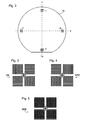
- Figure 2 shows a wafer W which is to be provided with devices on both sides and on which are provided normal markers (not shown) and reversed markers 1-4.
- the reversed markers 1-4 are mirror images - about the axis about which the wafer is to be rotated, in this case the Y axis - of the normal markers.
- the normal markers may take any convenient form, such as a grating, a group of gratings, box-in-box, frame-in-frame, chevrons, etc., as known in the art, and may form the primary markers used for global alignment of the substrate prior to a series of exposures. In the present example the markers are provided at symmetrical positions on the wafer axes.
- the present invention may of course also be applied to other markers, e.g. markers adjacent each target area or die.
- FIG 3 an example of a normal marker PM is shown - this comprises a group of four gratings. Of the four gratings, a pair are horizontal and a pair vertical and, though not apparent from the drawing, the two gratings of each pair have different periods in a known manner.
- Figure 4 shows the corresponding reversed marker RPM which has the same four gratings but in a mirror image arrangement.
- the combined marker OPM is shown in Figure 5 - as can be seen, the one-dimensional gratings become two-dimensional gratings or grids.
- Figures 6 to 8 illustrate steps in an example of the method of the invention.
- normal markers (not shown) and reversed markers OPM1, OPM2 are etched into first surface 10a of substrate W1 in a known manner to a depth d1 of 10 ⁇ m or more. Exposures and other process steps to form desired devices on the first surface are then performed.
- the substrate W1 is then flipped over and bonded to carrier substrate W2 with a layer of adhesive.
- Figure 7 shows the substrate W bonded to the carrier substrate CW, with the second surface 10b uppermost.
- the wafer W is ground or lapped to a desired thickness, d2, e.g. of about 10 ⁇ m or less, and the upper surface 10b' finished as required for the devices to be formed on it.
- d2 a desired thickness
- the reversed markers 1-4 which were etched to a depth of 10 ⁇ m or more into the first surface are revealed in the second surface and can be aligned to in a known manner.
Landscapes
- Physics & Mathematics (AREA)
- General Physics & Mathematics (AREA)
- Exposure And Positioning Against Photoresist Photosensitive Materials (AREA)
Priority Applications (1)
| Application Number | Priority Date | Filing Date | Title |
|---|---|---|---|
| EP20030258052 EP1469355B1 (fr) | 2002-12-20 | 2003-12-19 | Méthode de fabrication d'un dispositif |
Applications Claiming Priority (3)
| Application Number | Priority Date | Filing Date | Title |
|---|---|---|---|
| EP02258834 | 2002-12-20 | ||
| EP02258834 | 2002-12-20 | ||
| EP20030258052 EP1469355B1 (fr) | 2002-12-20 | 2003-12-19 | Méthode de fabrication d'un dispositif |
Publications (2)
| Publication Number | Publication Date |
|---|---|
| EP1469355A1 true EP1469355A1 (fr) | 2004-10-20 |
| EP1469355B1 EP1469355B1 (fr) | 2008-08-20 |
Family
ID=32910117
Family Applications (1)
| Application Number | Title | Priority Date | Filing Date |
|---|---|---|---|
| EP20030258052 Expired - Lifetime EP1469355B1 (fr) | 2002-12-20 | 2003-12-19 | Méthode de fabrication d'un dispositif |
Country Status (1)
| Country | Link |
|---|---|
| EP (1) | EP1469355B1 (fr) |
Citations (3)
| Publication number | Priority date | Publication date | Assignee | Title |
|---|---|---|---|---|
| US4818724A (en) * | 1986-06-30 | 1989-04-04 | Selenia Industrie Elettroniche Associate S.P.A. | Photolithographic method of aligning a structure on the back of a substrate |
| US5004705A (en) * | 1989-01-06 | 1991-04-02 | Unitrode Corporation | Inverted epitaxial process |
| EP1081748A2 (fr) * | 1999-08-30 | 2001-03-07 | Lucent Technologies Inc. | Arrêts de gravure et marques d'alignement pour des plaquettes soudées |
-
2003
- 2003-12-19 EP EP20030258052 patent/EP1469355B1/fr not_active Expired - Lifetime
Patent Citations (3)
| Publication number | Priority date | Publication date | Assignee | Title |
|---|---|---|---|---|
| US4818724A (en) * | 1986-06-30 | 1989-04-04 | Selenia Industrie Elettroniche Associate S.P.A. | Photolithographic method of aligning a structure on the back of a substrate |
| US5004705A (en) * | 1989-01-06 | 1991-04-02 | Unitrode Corporation | Inverted epitaxial process |
| EP1081748A2 (fr) * | 1999-08-30 | 2001-03-07 | Lucent Technologies Inc. | Arrêts de gravure et marques d'alignement pour des plaquettes soudées |
Also Published As
| Publication number | Publication date |
|---|---|
| EP1469355B1 (fr) | 2008-08-20 |
Similar Documents
| Publication | Publication Date | Title |
|---|---|---|
| KR100616601B1 (ko) | 디바이스 제조방법 | |
| EP1420300B1 (fr) | Appareil lithographique et méthode de fabrication d'un dispositif | |
| US9195153B2 (en) | Lithographic apparatus and device manufacturing method | |
| US7130049B2 (en) | Method of measurement, method for providing alignment marks, and device manufacturing method | |
| US7292339B2 (en) | Alignment method and apparatus, lithographic apparatus, device manufacturing method, and alignment tool | |
| US7251018B2 (en) | Substrate table, method of measuring a position of a substrate and a lithographic apparatus | |
| US6960775B1 (en) | Lithographic apparatus, device manufacturing method and device manufactured thereby | |
| KR100585210B1 (ko) | 디바이스 제조방법 및 그것에 의해 제조된 디바이스 | |
| US20060035159A1 (en) | Method of providing alignment marks, method of aligning a substrate, device manufacturing method, computer program, and device | |
| US20070070311A1 (en) | Contacts to microdevices | |
| US7193231B2 (en) | Alignment tool, a lithographic apparatus, an alignment method, a device manufacturing method and device manufactured thereby | |
| EP1469355B1 (fr) | Méthode de fabrication d'un dispositif | |
| EP1400860B1 (fr) | Structure d'une marque lithograhique, appareil de projection lithographique comprenant une telle structure et procédé d'alignement d'un substrat utilisant une telle structure | |
| EP1420449A1 (fr) | Méthode de fabrication d'un dispositif avec des marques d'alignement en revers | |
| NL1036096A1 (nl) | Lithographic method. | |
| JP4658004B2 (ja) | デバイス製造方法 | |
| JP4435760B2 (ja) | デバイス製造方法 | |
| EP1398670A2 (fr) | Procédé d'alignement d'un substrat, programme informatique et procédé pour la production d'un dispositif | |
| EP1396761A2 (fr) | Dispositif d'alignement, appareil lithographique, méthode d'alignement et méthode de fabrication d'un dispositif |
Legal Events
| Date | Code | Title | Description |
|---|---|---|---|
| PUAI | Public reference made under article 153(3) epc to a published international application that has entered the european phase |
Free format text: ORIGINAL CODE: 0009012 |
|
| AK | Designated contracting states |
Kind code of ref document: A1 Designated state(s): AT BE BG CH CY CZ DE DK EE ES FI FR GB GR HU IE IT LI LU MC NL PT RO SE SI SK TR |
|
| AX | Request for extension of the european patent |
Extension state: AL LT LV MK |
|
| 17P | Request for examination filed |
Effective date: 20050112 |
|
| AKX | Designation fees paid |
Designated state(s): DE FR GB IT NL |
|
| 17Q | First examination report despatched |
Effective date: 20070201 |
|
| GRAP | Despatch of communication of intention to grant a patent |
Free format text: ORIGINAL CODE: EPIDOSNIGR1 |
|
| GRAS | Grant fee paid |
Free format text: ORIGINAL CODE: EPIDOSNIGR3 |
|
| GRAA | (expected) grant |
Free format text: ORIGINAL CODE: 0009210 |
|
| AK | Designated contracting states |
Kind code of ref document: B1 Designated state(s): DE FR GB IT NL |
|
| REG | Reference to a national code |
Ref country code: GB Ref legal event code: FG4D |
|
| REF | Corresponds to: |
Ref document number: 60323051 Country of ref document: DE Date of ref document: 20081002 Kind code of ref document: P |
|
| PGFP | Annual fee paid to national office [announced via postgrant information from national office to epo] |
Ref country code: FR Payment date: 20081212 Year of fee payment: 6 |
|
| PGFP | Annual fee paid to national office [announced via postgrant information from national office to epo] |
Ref country code: DE Payment date: 20081219 Year of fee payment: 6 |
|
| PLBE | No opposition filed within time limit |
Free format text: ORIGINAL CODE: 0009261 |
|
| STAA | Information on the status of an ep patent application or granted ep patent |
Free format text: STATUS: NO OPPOSITION FILED WITHIN TIME LIMIT |
|
| 26N | No opposition filed |
Effective date: 20090525 |
|
| GBPC | Gb: european patent ceased through non-payment of renewal fee |
Effective date: 20081219 |
|
| NLV4 | Nl: lapsed or anulled due to non-payment of the annual fee |
Effective date: 20090701 |
|
| PG25 | Lapsed in a contracting state [announced via postgrant information from national office to epo] |
Ref country code: NL Free format text: LAPSE BECAUSE OF NON-PAYMENT OF DUE FEES Effective date: 20090701 Ref country code: GB Free format text: LAPSE BECAUSE OF NON-PAYMENT OF DUE FEES Effective date: 20081219 |
|
| REG | Reference to a national code |
Ref country code: FR Ref legal event code: ST Effective date: 20100831 |
|
| PG25 | Lapsed in a contracting state [announced via postgrant information from national office to epo] |
Ref country code: FR Free format text: LAPSE BECAUSE OF NON-PAYMENT OF DUE FEES Effective date: 20091231 |
|
| PG25 | Lapsed in a contracting state [announced via postgrant information from national office to epo] |
Ref country code: DE Free format text: LAPSE BECAUSE OF NON-PAYMENT OF DUE FEES Effective date: 20100701 |
|
| PG25 | Lapsed in a contracting state [announced via postgrant information from national office to epo] |
Ref country code: IT Free format text: LAPSE BECAUSE OF NON-PAYMENT OF DUE FEES Effective date: 20081219 |