EP1469710B1 - Support de composants et son procédé de fabrication - Google Patents
Support de composants et son procédé de fabrication Download PDFInfo
- Publication number
- EP1469710B1 EP1469710B1 EP20040002650 EP04002650A EP1469710B1 EP 1469710 B1 EP1469710 B1 EP 1469710B1 EP 20040002650 EP20040002650 EP 20040002650 EP 04002650 A EP04002650 A EP 04002650A EP 1469710 B1 EP1469710 B1 EP 1469710B1
- Authority
- EP
- European Patent Office
- Prior art keywords
- circuit
- carrier
- circuit carrier
- components
- component carrier
- Prior art date
- Legal status (The legal status is an assumption and is not a legal conclusion. Google has not performed a legal analysis and makes no representation as to the accuracy of the status listed.)
- Expired - Lifetime
Links
Images

Classifications
-
- H—ELECTRICITY
- H05—ELECTRIC TECHNIQUES NOT OTHERWISE PROVIDED FOR
- H05K—PRINTED CIRCUITS; CASINGS OR CONSTRUCTIONAL DETAILS OF ELECTRIC APPARATUS; MANUFACTURE OF ASSEMBLAGES OF ELECTRICAL COMPONENTS
- H05K1/00—Printed circuits
- H05K1/02—Details
- H05K1/14—Structural association of two or more printed circuits
- H05K1/141—One or more single auxiliary printed circuits mounted on a main printed circuit, e.g. modules, adapters
-
- H—ELECTRICITY
- H05—ELECTRIC TECHNIQUES NOT OTHERWISE PROVIDED FOR
- H05K—PRINTED CIRCUITS; CASINGS OR CONSTRUCTIONAL DETAILS OF ELECTRIC APPARATUS; MANUFACTURE OF ASSEMBLAGES OF ELECTRICAL COMPONENTS
- H05K2201/00—Indexing scheme relating to printed circuits covered by H05K1/00
- H05K2201/10—Details of components or other objects attached to or integrated in a printed circuit board
- H05K2201/10227—Other objects, e.g. metallic pieces
- H05K2201/10295—Metallic connector elements partly mounted in a hole of the PCB
- H05K2201/10303—Pin-in-hole mounted pins
-
- H—ELECTRICITY
- H05—ELECTRIC TECHNIQUES NOT OTHERWISE PROVIDED FOR
- H05K—PRINTED CIRCUITS; CASINGS OR CONSTRUCTIONAL DETAILS OF ELECTRIC APPARATUS; MANUFACTURE OF ASSEMBLAGES OF ELECTRICAL COMPONENTS
- H05K2201/00—Indexing scheme relating to printed circuits covered by H05K1/00
- H05K2201/10—Details of components or other objects attached to or integrated in a printed circuit board
- H05K2201/10227—Other objects, e.g. metallic pieces
- H05K2201/10409—Screws
-
- H—ELECTRICITY
- H05—ELECTRIC TECHNIQUES NOT OTHERWISE PROVIDED FOR
- H05K—PRINTED CIRCUITS; CASINGS OR CONSTRUCTIONAL DETAILS OF ELECTRIC APPARATUS; MANUFACTURE OF ASSEMBLAGES OF ELECTRICAL COMPONENTS
- H05K2201/00—Indexing scheme relating to printed circuits covered by H05K1/00
- H05K2201/10—Details of components or other objects attached to or integrated in a printed circuit board
- H05K2201/10431—Details of mounted components
- H05K2201/10606—Permanent holder for component or auxiliary printed circuits mounted on a printed circuit board [PCB]
-
- H—ELECTRICITY
- H05—ELECTRIC TECHNIQUES NOT OTHERWISE PROVIDED FOR
- H05K—PRINTED CIRCUITS; CASINGS OR CONSTRUCTIONAL DETAILS OF ELECTRIC APPARATUS; MANUFACTURE OF ASSEMBLAGES OF ELECTRICAL COMPONENTS
- H05K2201/00—Indexing scheme relating to printed circuits covered by H05K1/00
- H05K2201/10—Details of components or other objects attached to or integrated in a printed circuit board
- H05K2201/10613—Details of electrical connections of non-printed components, e.g. special leads
- H05K2201/10742—Details of leads
- H05K2201/1075—Shape details
- H05K2201/10757—Bent leads
-
- H—ELECTRICITY
- H05—ELECTRIC TECHNIQUES NOT OTHERWISE PROVIDED FOR
- H05K—PRINTED CIRCUITS; CASINGS OR CONSTRUCTIONAL DETAILS OF ELECTRIC APPARATUS; MANUFACTURE OF ASSEMBLAGES OF ELECTRICAL COMPONENTS
- H05K2201/00—Indexing scheme relating to printed circuits covered by H05K1/00
- H05K2201/20—Details of printed circuits not provided for in H05K2201/01 - H05K2201/10
- H05K2201/2018—Presence of a frame in a printed circuit or printed circuit assembly
-
- H—ELECTRICITY
- H05—ELECTRIC TECHNIQUES NOT OTHERWISE PROVIDED FOR
- H05K—PRINTED CIRCUITS; CASINGS OR CONSTRUCTIONAL DETAILS OF ELECTRIC APPARATUS; MANUFACTURE OF ASSEMBLAGES OF ELECTRICAL COMPONENTS
- H05K2201/00—Indexing scheme relating to printed circuits covered by H05K1/00
- H05K2201/20—Details of printed circuits not provided for in H05K2201/01 - H05K2201/10
- H05K2201/2036—Permanent spacer or stand-off in a printed circuit or printed circuit assembly
-
- H—ELECTRICITY
- H05—ELECTRIC TECHNIQUES NOT OTHERWISE PROVIDED FOR
- H05K—PRINTED CIRCUITS; CASINGS OR CONSTRUCTIONAL DETAILS OF ELECTRIC APPARATUS; MANUFACTURE OF ASSEMBLAGES OF ELECTRICAL COMPONENTS
- H05K3/00—Apparatus or processes for manufacturing printed circuits
- H05K3/30—Assembling printed circuits with electric components, e.g. with resistors
- H05K3/301—Assembling printed circuits with electric components, e.g. with resistors by means of a mounting structure
-
- H—ELECTRICITY
- H05—ELECTRIC TECHNIQUES NOT OTHERWISE PROVIDED FOR
- H05K—PRINTED CIRCUITS; CASINGS OR CONSTRUCTIONAL DETAILS OF ELECTRIC APPARATUS; MANUFACTURE OF ASSEMBLAGES OF ELECTRICAL COMPONENTS
- H05K3/00—Apparatus or processes for manufacturing printed circuits
- H05K3/30—Assembling printed circuits with electric components, e.g. with resistors
- H05K3/303—Assembling printed circuits with electric components, e.g. with resistors with surface mounted components
- H05K3/305—Affixing by adhesive
-
- H—ELECTRICITY
- H05—ELECTRIC TECHNIQUES NOT OTHERWISE PROVIDED FOR
- H05K—PRINTED CIRCUITS; CASINGS OR CONSTRUCTIONAL DETAILS OF ELECTRIC APPARATUS; MANUFACTURE OF ASSEMBLAGES OF ELECTRICAL COMPONENTS
- H05K3/00—Apparatus or processes for manufacturing printed circuits
- H05K3/30—Assembling printed circuits with electric components, e.g. with resistors
- H05K3/32—Assembling printed circuits with electric components, e.g. with resistors electrically connecting electric components or wires to printed circuits
- H05K3/34—Assembling printed circuits with electric components, e.g. with resistors electrically connecting electric components or wires to printed circuits by soldering
- H05K3/3447—Lead-in-hole components
Definitions
- the invention relates to a component carrier and a method for producing such a component carrier.
- a disadvantage of this technique is that it requires high tool and investment costs, with changes in the entire lead frame and the plastic encapsulation must be reconfigured. It is also unfavorable that during welding, the connection of the component to the stamped grid takes place serially, that is to say that each welding takes place separately and therefore long cycle times are present.
- the size of the component carrier produced by the stamped grid process is due to technical limitations only limited, whereby the Scdazzlingl or the Scdazzlingltaug naval of the finished component carrier is in need of improvement.
- the object of the invention is to make available a component carrier and a method for the production thereof in which the advantages of an increased layout design possibility are combined with those of an improved shaking behavior.
- the component carrier Due to the inventive design of the component carrier, it is advantageously possible to realize by dividing the circuit substrate into several sections and a sheet-like arrangement in several levels, while with a stamped grid only one level is available for layouts. As a result, the possibilities of layout design of the circuit are considerably increased.
- the device carrier according to the invention is much less sensitive to changes in component and layout, because only a change in the circuit layout is required, while in the stamped grid technology a complete redesign of stamped grid and encapsulation is necessary.
- circuit carriers instead of lead frames also makes it possible to improve the EMC behavior since short cable runs can be provided at EMC-critical circuit areas and EMC-improving circuit measures, such as, for example, EMC capacitors or similar, can be used.
- the inventive design of the device carrier allows a removal of circuit parts to different circuit carriers, whereby a space gain on a main circuit carrier or a main circuit board is possible, which is reflected also in a cost reduction.
- Another advantage is that the component carrier can be produced in a reduced size, since welding tabs are eliminated.
- the reduction in size is favorable for improving the shaking performance.
- the packaging density can advantageously be increased, which in turn benefits the reduction of the size.
- a further advantage in the production of the component carrier according to the invention is the achievable cycle time reduction, the circuit carrier and wired components and special components can be connected together in one operation, for example by partial soldering.
- the first and / or the second circuit carrier are formed with a printed circuit board, a flexible film or the like without the conventional stamped grid.
- the charging connection with low rigidity is formed with a pin, preferably a punched grid pin, which has a geometry for mechanical relief.
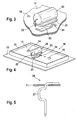
- FIG. 1 an embodiment of a component carrier 10 is shown, which consists of a first circuit carrier 11, a space-shaped receiving device 12 and a second circuit carrier 13. Die beiden Anlagenscht 11, 12 Sind jeweils in dem Gescousemik 12 anrob. With 14 and 15 screws are shown, with which the first circuit substrate 11 are screwed into correspondingly provided sterabilityn 16 and 17 through holes 18 and 19 in the first circuit substrate 11 for attaching the circuit substrate 11 to the frame-shaped receiving device 12.
- a preferably releasable latching in the receiving device 12 or a gluing of the circuit carrier 11 in the receiving device 12 may be provided.
- the receiving device 12 is on the second circuit carrier 13, for example attached by gluing. Alternatively, it can also be screwed and / or glued.
- the receptacle 12 formed as a frame-shaped holder is made of plastic, but could also be made of die-cast, sheet metal or the like.
- FIG. 3 Exemplary is enlarged in FIG. 3 the attachment of a wired component 20 on the first circuit substrate 11 by means of a large-area applied adhesive 21 is shown.
- the component 20 has on both sides or on one side only a wiring 22, which are usually carried out through a hole in the circuit substrate 11 for later soldering.
- a sheet-metal stamped part 23 is shown, which rests on the first circuit carrier 11 and has a curved portion 24 as a mechanical relief, which merges into a vertical portion which passes through a bore, not shown, of the first circuit substrate 11 and as a conductor connection to the second circuit carrier thirteenth is trained. Due to the mechanical relief, a reduced rigidity of the line connection is achieved.
- FIG. 4 shows the assembled component carrier 10 in an oblique plan view, wherein it can be seen that the first circuit carrier, which is designed as a printed circuit board, is received in the rectangular space-shaped holder 12 and securely abuts against a contact shoulder 25.
- the first circuit carrier which is designed as a printed circuit board
- the frame-shaped holder 12 may also be modified to the effect that it can be used for mutual reception of circuit carriers.
- FIG. 5 shows an embodiment of a conductor connection 26, in which a mechanical relief portion 27 is disposed in the region between the first and second circuit carrier.
- an electrical circuit is distributed to at least two circuit carriers, preferably printed circuit boards, wherein a first circuit carrier or a first circuit board preferably for loading with wired components and special components and a second circuit carrier none or only a few leaded components and special components, but SMD components, such as ICs or the like. If required, more than one first or second circuit carrier may also be provided. Furthermore, SMD components can also be provided on the first printed circuit board.
- the or the first circuit carrier as provided, equipped with wired components and special components and then electrically contacted the components by soldering.
- a receiving device which may be formed in a suitable manner, for example as a holder or preferably as a frame-shaped holder.
- the receiving device is then attached to the second circuit carrier and then the first circuit carrier is electrically connected to the second circuit carrier via at least one conductor of low rigidity.
Landscapes
- Engineering & Computer Science (AREA)
- Microelectronics & Electronic Packaging (AREA)
- Combinations Of Printed Boards (AREA)
- Shielding Devices Or Components To Electric Or Magnetic Fields (AREA)
Claims (10)
- Porte-composants (10) constitué de :au moins un premier porte-circuit (11) équipé de composants électriques (20) câblés et de composants spéciaux,un dispositif (12) qui loge au moins un premier porte-circuit (11) etun deuxième porte-circuit (13) situé à distance du premier porte-circuit, sans composants électriques câblés ni composants spéciaux ou avec seulement un petit nombre de ceux-ci,le deuxième porte-circuit (13) étant raccordé électriquement à chaque premier porte-circuit (11) au moyen d'au moins une liaison conductrice (26) à faible rigidité,
caractérisé en ce quela liaison conductrice (26) à faible rigidité est configurée avec au moins un goujon, de préférence un goujon de grille estampé dont la géométrie permet un délestage mécanique. - Porte-composants selon la revendication 1, caractérisé en ce que le premier et/ou le deuxième porte-circuit présentent une carte de circuit, une feuille flexible ou similaire.
- Porte-composants selon les revendications 1 ou 2, caractérisé en ce que les composants câblés (20) et les composants spéciaux sont fixés sur le premier porte-circuit au moyen d'un adhésif (21) et/ou d'un support séparé.
- Porte-composants selon l'une des revendications précédentes, caractérisé en ce que deux premiers porte-circuits (11) sont disposés sur le dispositif de réception (12).
- Porte-composants selon l'une des revendications précédentes, caractérisé en ce que le dispositif de réception (12) est configuré en forme d'encadrement ou de support plat.
- Porte-composants selon l'une des revendications précédentes, caractérisé en ce que le dispositif de réception (12) est formé de matière synthétique, de fonte ou de tôle.
- Porte-composants selon l'une des revendications précédentes, caractérisé en ce qu'au moins un emplacement de raccordement pour la liaison conductrice (26) est formé sur chaque premier porte-circuit (11).
- Porte-composants selon l'une des revendications précédentes, caractérisé en ce que la liaison conductrice (26) dont la géométrie permet un délestage mécanique présente une partie mécanique de délestage (27) dans sa partie située entre le premier et le deuxième porte-circuit.
- Procédé de fabrication d'un porte-composants électrique, le procédé étant constitué des étapes suivantes :répartition d'un circuit électrique sur au moins deux porte-circuits, au moins un premier porte-circuit étant prévu de préférence pour être équipé de composants câblés et de composants spéciaux et un deuxième porte-circuit étant prévu de préférence sans ou avec peu de composants câblés et de composants spéciaux,équipement du premier porte-circuit et établissement du contact électrique par brasage,fixation du ou des premiers porte-circuits sur un dispositif de réception,fixation du dispositif de réception sur le deuxième porte-circuit etraccordement électrique du premier porte-circuit et du deuxième porte-circuit par au moins un conducteur à faible rigidité,le conducteur étant configuré avec au moins un goujon, de préférence un goujon de grille estampée, dont la géométrie permet un délestage mécanique.
- Procédé selon la revendication 9, caractérisé en ce que le premier et/ou le deuxième porte-circuit sont configurés avec une carte de circuit ou une feuille stratifiée sur un support métallique.
Applications Claiming Priority (2)
| Application Number | Priority Date | Filing Date | Title |
|---|---|---|---|
| DE2003117095 DE10317095A1 (de) | 2003-04-14 | 2003-04-14 | Bauelemententräger und Verfahren zu dessen Herstellung |
| DE10317095 | 2003-04-14 |
Publications (3)
| Publication Number | Publication Date |
|---|---|
| EP1469710A2 EP1469710A2 (fr) | 2004-10-20 |
| EP1469710A3 EP1469710A3 (fr) | 2006-01-11 |
| EP1469710B1 true EP1469710B1 (fr) | 2012-09-05 |
Family
ID=32892338
Family Applications (1)
| Application Number | Title | Priority Date | Filing Date |
|---|---|---|---|
| EP20040002650 Expired - Lifetime EP1469710B1 (fr) | 2003-04-14 | 2004-02-06 | Support de composants et son procédé de fabrication |
Country Status (2)
| Country | Link |
|---|---|
| EP (1) | EP1469710B1 (fr) |
| DE (1) | DE10317095A1 (fr) |
Families Citing this family (2)
| Publication number | Priority date | Publication date | Assignee | Title |
|---|---|---|---|---|
| ITTO20030754A1 (it) * | 2003-09-29 | 2005-03-30 | Gate Srl | Unita' elettronica di controllo, in particolare unita' |
| DE102018214441A1 (de) * | 2018-08-27 | 2020-02-27 | Continental Automotive Gmbh | Verfahren zur Herstellung einer Statorbaugruppe und Statorbaugruppe |
Family Cites Families (8)
| Publication number | Priority date | Publication date | Assignee | Title |
|---|---|---|---|---|
| FR2582898B1 (fr) * | 1985-06-04 | 1989-07-28 | Radiotechnique Compelec | Carte pour realiser un systeme de micro-informatique. |
| JPH01154592A (ja) * | 1987-12-11 | 1989-06-16 | Nec Corp | プリント板への部品実装方法 |
| DE3805121A1 (de) * | 1988-02-18 | 1989-08-31 | Siemens Ag | Entlastete, insbesondere zug- und druckentlastete loetverbindung |
| DE4405578B4 (de) * | 1994-02-22 | 2004-02-05 | Siemens Ag | Elektronische Baueinheit |
| DE19605966A1 (de) * | 1996-02-17 | 1997-08-21 | Bosch Gmbh Robert | Vorrichtung, insbesondere zur Verwendung in einem elektronischen Steuergerät |
| DE19756345C2 (de) * | 1997-12-18 | 1999-12-30 | Telefunken Microelectron | Anordnung zur Kontaktierung von Leiterplatten |
| GB9929168D0 (en) * | 1999-12-09 | 2000-02-02 | Matra Marconi Space Uk Ltd | Mounting electrical devices to circuit boards |
| US20030035280A1 (en) * | 2001-08-17 | 2003-02-20 | Malone Christopher Gregory | Daughter-card structural support |
-
2003
- 2003-04-14 DE DE2003117095 patent/DE10317095A1/de not_active Withdrawn
-
2004
- 2004-02-06 EP EP20040002650 patent/EP1469710B1/fr not_active Expired - Lifetime
Also Published As
| Publication number | Publication date |
|---|---|
| EP1469710A2 (fr) | 2004-10-20 |
| EP1469710A3 (fr) | 2006-01-11 |
| DE10317095A1 (de) | 2004-11-11 |
Similar Documents
| Publication | Publication Date | Title |
|---|---|---|
| EP1152368B1 (fr) | Carte à puce | |
| DE68905475T2 (de) | Halbleiter-speichermodul hoeher dichte. | |
| EP2684433B1 (fr) | Module comprenant un support, un composant cms et une partie grille estampée | |
| EP0924971B1 (fr) | Dispositif pour la connexion de plaques à circuit imprimé | |
| DE4430798A1 (de) | Stanzgitter zur Verbindung von elektrischen Bauelementen | |
| EP1484950A2 (fr) | Méthode de mise en contact èlectrique | |
| DE10250538A1 (de) | Elektronisches Bauteil als Multichipmodul und Verfahren zu dessen Herstellung | |
| DE19600928A1 (de) | Vorrichtung zur Handhabung von Leiterplatten und deren Herstellung | |
| DE2849418A1 (de) | Elektrischer verbinder zum verbinden einer elektronischen baueinheit mit einem traeger | |
| DE102006016775A1 (de) | Elektronische Vorrichtung und Verfahren zum Herstellen der Gleichen | |
| EP1245933A2 (fr) | Dispositif électromécanique pour le montage d' un équipement électronique sur un support, en particulier pour le montage d' un instrument indicateur encastré dans un tableau de bord | |
| EP1365640A2 (fr) | Bo tier et blindage électromagnétiques pour composants électroniques | |
| DE2828146A1 (de) | Elektrische leiterplatte | |
| EP0828412B1 (fr) | Module haute fréquence, par exemple syntoniseur | |
| EP1469710B1 (fr) | Support de composants et son procédé de fabrication | |
| DE102007035794A1 (de) | Leiterplattenverbund sowie Verfahren zum Herstellen eines Leiterplattenverbundes | |
| DE19800928B4 (de) | Gehäuse, insbesondere stapelbares Gehäuse, zur Aufnahme von Bauelementen und Verfahren zu dessen Herstellung | |
| DE102016010066B3 (de) | Abschirmungssystem mit an einem Substrat ausgebildetem Stützelement und Verfahren zum Herstellen des Systems | |
| DE19601202A1 (de) | Datenträgerkarte und Verfahren zu deren Herstellung | |
| DE19730417C1 (de) | Befestigungsmittel für Abschirmgehäuse von elektrischen Leiterplatten und Verfahren zu seiner Herstellung | |
| DE4405578B4 (de) | Elektronische Baueinheit | |
| DE10038390C1 (de) | Funktionell asymmetrische Schaltungsträgeranordnung mit spiegelsymmetrischer Bauteileanordnung | |
| DE60201537T2 (de) | Elektrische verbindungsanordnung für elektronische bauteile | |
| DE102005048097A1 (de) | Steuergeräteanordnung | |
| DE19618481C1 (de) | Elektronikmodul mit Steckkontakten und leitender Abdeckkappe |
Legal Events
| Date | Code | Title | Description |
|---|---|---|---|
| PUAI | Public reference made under article 153(3) epc to a published international application that has entered the european phase |
Free format text: ORIGINAL CODE: 0009012 |
|
| AK | Designated contracting states |
Kind code of ref document: A2 Designated state(s): AT BE BG CH CY CZ DE DK EE ES FI FR GB GR HU IE IT LI LU MC NL PT RO SE SI SK TR |
|
| AX | Request for extension of the european patent |
Extension state: AL LT LV MK |
|
| PUAL | Search report despatched |
Free format text: ORIGINAL CODE: 0009013 |
|
| AK | Designated contracting states |
Kind code of ref document: A3 Designated state(s): AT BE BG CH CY CZ DE DK EE ES FI FR GB GR HU IE IT LI LU MC NL PT RO SE SI SK TR |
|
| AX | Request for extension of the european patent |
Extension state: AL LT LV MK |
|
| 17P | Request for examination filed |
Effective date: 20060711 |
|
| AKX | Designation fees paid |
Designated state(s): DE FR IT |
|
| 17Q | First examination report despatched |
Effective date: 20110204 |
|
| GRAP | Despatch of communication of intention to grant a patent |
Free format text: ORIGINAL CODE: EPIDOSNIGR1 |
|
| GRAS | Grant fee paid |
Free format text: ORIGINAL CODE: EPIDOSNIGR3 |
|
| GRAA | (expected) grant |
Free format text: ORIGINAL CODE: 0009210 |
|
| AK | Designated contracting states |
Kind code of ref document: B1 Designated state(s): DE FR IT |
|
| REG | Reference to a national code |
Ref country code: DE Ref legal event code: R096 Ref document number: 502004013728 Country of ref document: DE Effective date: 20121025 |
|
| PLBE | No opposition filed within time limit |
Free format text: ORIGINAL CODE: 0009261 |
|
| STAA | Information on the status of an ep patent application or granted ep patent |
Free format text: STATUS: NO OPPOSITION FILED WITHIN TIME LIMIT |
|
| 26N | No opposition filed |
Effective date: 20130606 |
|
| REG | Reference to a national code |
Ref country code: DE Ref legal event code: R097 Ref document number: 502004013728 Country of ref document: DE Effective date: 20130606 |
|
| REG | Reference to a national code |
Ref country code: FR Ref legal event code: PLFP Year of fee payment: 13 |
|
| PGFP | Annual fee paid to national office [announced via postgrant information from national office to epo] |
Ref country code: IT Payment date: 20160222 Year of fee payment: 13 |
|
| PGFP | Annual fee paid to national office [announced via postgrant information from national office to epo] |
Ref country code: FR Payment date: 20160222 Year of fee payment: 13 |
|
| REG | Reference to a national code |
Ref country code: FR Ref legal event code: ST Effective date: 20171031 |
|
| PG25 | Lapsed in a contracting state [announced via postgrant information from national office to epo] |
Ref country code: FR Free format text: LAPSE BECAUSE OF NON-PAYMENT OF DUE FEES Effective date: 20170228 |
|
| PG25 | Lapsed in a contracting state [announced via postgrant information from national office to epo] |
Ref country code: IT Free format text: LAPSE BECAUSE OF NON-PAYMENT OF DUE FEES Effective date: 20170206 |
|
| PGFP | Annual fee paid to national office [announced via postgrant information from national office to epo] |
Ref country code: DE Payment date: 20230426 Year of fee payment: 20 |
|
| REG | Reference to a national code |
Ref country code: DE Ref legal event code: R071 Ref document number: 502004013728 Country of ref document: DE |