EP1473581A2 - Dispositif d'affichage par pixel à interférence optique avec contrôle de charge - Google Patents
Dispositif d'affichage par pixel à interférence optique avec contrôle de charge Download PDFInfo
- Publication number
- EP1473581A2 EP1473581A2 EP03024950A EP03024950A EP1473581A2 EP 1473581 A2 EP1473581 A2 EP 1473581A2 EP 03024950 A EP03024950 A EP 03024950A EP 03024950 A EP03024950 A EP 03024950A EP 1473581 A2 EP1473581 A2 EP 1473581A2
- Authority
- EP
- European Patent Office
- Prior art keywords
- reflector
- electronic device
- optical cavity
- reflectors
- pixel
- Prior art date
- Legal status (The legal status is an assumption and is not a legal conclusion. Google has not performed a legal analysis and makes no representation as to the accuracy of the status listed.)
- Withdrawn
Links
Images


Classifications
-
- G—PHYSICS
- G09—EDUCATION; CRYPTOGRAPHY; DISPLAY; ADVERTISING; SEALS
- G09G—ARRANGEMENTS OR CIRCUITS FOR CONTROL OF INDICATING DEVICES USING STATIC MEANS TO PRESENT VARIABLE INFORMATION
- G09G3/00—Control arrangements or circuits, of interest only in connection with visual indicators other than cathode-ray tubes
- G09G3/20—Control arrangements or circuits, of interest only in connection with visual indicators other than cathode-ray tubes for presentation of an assembly of a number of characters, e.g. a page, by composing the assembly by combination of individual elements arranged in a matrix no fixed position being assigned to or needed to be assigned to the individual characters or partial characters
- G09G3/34—Control arrangements or circuits, of interest only in connection with visual indicators other than cathode-ray tubes for presentation of an assembly of a number of characters, e.g. a page, by composing the assembly by combination of individual elements arranged in a matrix no fixed position being assigned to or needed to be assigned to the individual characters or partial characters by control of light from an independent source
- G09G3/3433—Control arrangements or circuits, of interest only in connection with visual indicators other than cathode-ray tubes for presentation of an assembly of a number of characters, e.g. a page, by composing the assembly by combination of individual elements arranged in a matrix no fixed position being assigned to or needed to be assigned to the individual characters or partial characters by control of light from an independent source using light modulating elements actuated by an electric field and being other than liquid crystal devices and electrochromic devices
- G09G3/3466—Control arrangements or circuits, of interest only in connection with visual indicators other than cathode-ray tubes for presentation of an assembly of a number of characters, e.g. a page, by composing the assembly by combination of individual elements arranged in a matrix no fixed position being assigned to or needed to be assigned to the individual characters or partial characters by control of light from an independent source using light modulating elements actuated by an electric field and being other than liquid crystal devices and electrochromic devices based on interferometric effect
-
- G—PHYSICS
- G02—OPTICS
- G02B—OPTICAL ELEMENTS, SYSTEMS OR APPARATUS
- G02B26/00—Optical devices or arrangements for the control of light using movable or deformable optical elements
- G02B26/001—Optical devices or arrangements for the control of light using movable or deformable optical elements based on interference in an adjustable optical cavity
-
- G—PHYSICS
- G09—EDUCATION; CRYPTOGRAPHY; DISPLAY; ADVERTISING; SEALS
- G09G—ARRANGEMENTS OR CIRCUITS FOR CONTROL OF INDICATING DEVICES USING STATIC MEANS TO PRESENT VARIABLE INFORMATION
- G09G2300/00—Aspects of the constitution of display devices
- G09G2300/08—Active matrix structure, i.e. with use of active elements, inclusive of non-linear two terminal elements, in the pixels together with light emitting or modulating elements
- G09G2300/0809—Several active elements per pixel in active matrix panels
Definitions
- Such conventional displays include direct view and projection cathode-ray tube (CRT) displays, direct view and projection liquid crystal displays (LCD's), direct view plasma displays, projection digital light processing (DLP) displays, and direct view electroluminescent (EL) displays, among others.
- CTR cathode-ray tube
- LCD direct view and projection liquid crystal displays
- DLP projection digital light processing
- EL direct view electroluminescent
- An electronic device of an embodiment of the invention is for at least partially displaying a pixel of a displayable image.
- the electronic device includes a first reflector and a second reflector that define an optical cavity therebetween, and which is selective of a visible wavelength at an intensity by optical interference.
- the electronic device also includes a charge-controlling mechanism to allow optical properties of the optical cavity to be varied by controlling a predetermined amount of charge stored on the first and the second reflectors. The visible wavelength and/or the intensity are thus variably selectable in correspondence with the pixel of the displayable image.
- FIG. 1A is a diagram of an electronic device for at least partially displaying a pixel of a displayable image, according to an embodiment of the invention.
- FIGs. 1B, 1C, and 1D are diagrams showing different approaches to control the charge stored on the electronic device of FIG. 1A, according to varying embodiments of the invention.
- FIG. 3A is a diagram of an array of passive pixel mechanisms, according to an embodiment of the invention.
- FIG. 6 is a method of manufacture, according to an embodiment of the invention.
- FIGs. 7A, 7B, and 7C are diagrams of electronic devices that are more specific than but consistent with the electronic device of FIG. 1A, according to varying embodiments of the invention.
- FIGs. 8A and 8B are diagrams of electronic devices that are more specific than but consistent with the electronic device of FIG. 1A, and which include lenses, according to varying embodiments of the invention.
- FIGs. 9A, 9B, and 9C are diagrams illustratively depicting how anti-stiction bumps can be fabricated within the electronic device of FIG. 1A, according to an embodiment of the invention.
- FIGs. 10A, 10B, and 10C are diagrams illustratively depicting how anti-stiction bumps can be fabricated within the electronic device of FIG. 1A, according to another embodiment of the invention.
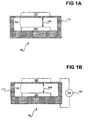
- FIG. 1A shows an electronic device 100 for at least partially displaying a pixel of a displayable image, according to an embodiment of the invention.
- the device 100 includes a top reflector 102 and a bottom reflector 104, as well as a flexure 110 and a spring mechanism 112.
- a resonant optical cavity 106 is defined by the reflectors 102 and 104, which has a variable thickness, or width, 108.
- the top reflector 102 is in one embodiment highly reflective, such as completely reflective.
- the bottom reflector 104 is in one embodiment semitransparent; that is, the bottom reflector 104 is in one embodiment semi-reflective.
- the spring mechanism 112 may be a flexible material, such as a polymer, in one embodiment of the invention, that has linear or non-linear spring functionality.
- the flexure 110 and the spring mechanism 112 allow the thickness 108 of the cavity 106 to vary, by allowing the bottom reflector 104 to move. More generally, the flexure 110 and the spring mechanism 112 constitute a mechanism that allows variation of the optical properties of the optical cavity 106 to variably select a visible wavelength at an intensity.
- the optical properties include the optical index of the cavity 106, and/or the optical thickness of the cavity 106.
- a voltage applied between the reflectors 102 and 104, or electrical charge stored on the reflectors 102 and 104, causes the thickness 108 of the cavity 106 to change, because the flexure 110 and the spring mechanism 112 allow the reflector 104 to move.
- the flexure 110 has a stiffness
- the spring mechanism 112 has a spring restoring force, such that the voltage applied to the reflectors 102 and 104 or the charge stored on the reflectors 102 and 104 causes the flexure 110 and the spring mechanism 112 to yield and allow the reflector 104 to move, achieving the desired thickness 108. No power is dissipated in maintaining a given thickness 108.
- the bottom reflector 104 is maintained at a fixed voltage, and the top reflector 102 is set to a voltage depending on the desired visible wavelength and the desired intensity, as calibrated to the stiffness of the flexure 110.
- the flexure 110 is shown in the embodiment of FIG. 1A as positioned under the bottom reflector 104, in another embodiment it may be positioned over the bottom reflector 104. In other embodiments, the flexure 110 may be positioned over or under the top reflector 102 as well, such that the bottom reflector 104 is movable, instead of the top reflector 102, to adjust the thickness 108 of the optical cavity 106.
- the bottom reflector 104 and the top reflector 102 can be considered the plates of a capacitor, where the optical cavity 106 represents the dielectric therebetween.
- a potential applied between the bottom reflector 104 and the top reflector 102 moves the bottom reflector 104, due to the flexure 110 and the spring mechanism 112, but also causes a charge to be stored in the capacitor. It is this electrostatic charge that then allows maintenance of the given thickness 108 without any further voltage application over the bottom reflector 104 and the top reflector 102.
- the wavelength and the intensity selected by the optical cavity 106 correspond to a pixel of a displayable image.
- the electronic device 100 at least partially displays the pixel of the image.
- the electronic device 100 can operate in either an analog or a digital manner.
- the electronic device 100 selects a visible wavelength of light and an intensity corresponding to the color and the intensity of the color of the pixel.
- the electronic device 100 may be used to display the pixel in an analog manner in black-and-white, or in gray scale, in lieu of color.
- this film stack sequence can achieve a green wavelength of 5500 ⁇ with an incident n of 1.5 at the top reflector 102 and a substrate n of 1.52 at the bottom reflector 104 in accordance with the following table: Layers Real index ( n ) Imaginary index ( k ) Thickness ( ⁇ ) Target wavelength intensity Number of waves at target Bottom reflector 104 (silver) 0.2 5 6250 5000 0.25 Optical cavity 106 1 0 2500 5000 0.5 Top reflector 102 (titanium) 2.5 2.5 200 5000 0.1
- the film stack sequence can also achieve a blue wavelength of 4500 ⁇ with an incident n of 1.5 at the top reflector 102 and a substrate n of 1.52 at the bottom reflector 104 in accordance with the following table: Layers Real index ( n ) Imaginary index ( k ) Thickness ( ⁇ ) Target wavelength intensity Number of waves at target Bottom reflector 104 (silver) 0.2 5 6250 5000 0.25 Optical cavity 106 1 0 2000 5000 0.5 Top reflector 102 (titanium) 2.5 2.5 200 5000 0.1
- the film stack sequence achieves a red wavelength of 6100 ⁇ , a green wavelength of 5500 ⁇ , or a blue wavelength of 4500 ⁇ , depending on whether the thickness of the optical cavity 106 is 2750 ⁇ , 2500 ⁇ , or 2000 ⁇ , respectively.
- the flexure 110 and the spring mechanism 112 allow the thickness 108 of the optical cavity 106 to vary when an appropriate voltage has been applied across the reflectors 102 and 104, such that a desired wavelength at a desired intensity is selected.
- N 7 x 10 -7 Newton
- a small voltage between the reflectors 102 and 104 provides sufficient force to move the bottom reflector 104, and hold it against gravity and shocks.
- the electrostatic charge stored in the capacitor created by the reflectors 102 and 104, and defining the cavity 106 is sufficient to hold the bottom reflector 104 in place without additional power. Charge leakage may require occasional refreshing of the charge, however.
- the force F is now not a function of the distance d , and stability of the reflector 104 can exist over the entire range of 0 to d 0 .
- the position of the reflector 104 can be set over the entire range of travel.
- the range within which non-contact operation can occur without snap down may be increased by constructing the flexure 110 in a particular manner.
- the particular manner is such that the restoring force of the spring mechanism 112 is a non-linear function of the displacement of the flexure 110, and increases at a faster rate than the displacement. This can be achieved by increasing the thickness of the flexure 110, or by using a flexure that is first bent and then stretched, which is known as a "bend and stretch" design.
- the device 100 can be operated at smaller values of the thickness 108, allowing a black state to be achieved without any portion of the reflectors 102 and 104 coming into contact with one another. This prevents stiction and the accompanying hysteresis that occurs when the reflectors 102 and 104 contact one another. Even if the reflectors 102 and 104 are allowed to contact one another, the voltage difference between the reflectors 102 and 104 will be less where the amount of charge on the reflectors 102 and 104 is specifically controlled (that is, where a predetermined amount of fixed charge is controlled), as opposed to where the voltage between the reflectors 102 and 104 is specifically controlled.
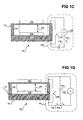
- FIGs. 1B, 1C, and 1D show different approaches to control the amount of charge on the reflectors 102 and 104 of the electronic device 100, as opposed to specifically controlling the voltage between the reflectors 102, and 104, according to varying embodiments of the invention.
- the thickness 108 between the reflectors 102 and 104 can be regulated by controlling the charge stored on the reflectors 102 and 104.
- the reflectors 102 and 104 thus act as the plates of a parallel plate capacitor.
- a controlled, or predetermined, amount of charge is injected onto the reflectors 102 and 104 by integrating a known current for a known time, utilizing the current integration mechanism 120 electrically coupled to the reflectors 102 and 104.
- the current, I, the time, t, or both the current and the time can thus be manipulated to yield the desired amount of charge.
- the mechanism 120 may include a current source, a digital-to-analog current source, and/or time division circuitry to create the desired level of charge.
- the charge available to the reflectors 102 and 104 is limited to prevent snap down of the reflectors 102 and 104 together.
- the circuit 129 includes a voltage source 130 placed in series with a capacitor 134.
- a switch 132 controls the on-off operation of the circuit 129.
- a switch 136 placed in parallel with the voltage source 130 and the capacitor 134, acts as a reset switch, which may be utilized to avoid voltage or charge drift over time, due to charge leakage. The reset is desirably performed more quickly than the mechanical response time of the circuit 129.
- the range of stable travel can be extended through the entire initial thickness 108 of the optical cavity 106 if C ⁇ C ' init / 2, where C is the capacitance of the capacitor 134, and C' init is the initial capacitance of the variable capacitor formed by the reflectors 102 and 104, and the optical cavity 106.
- C is the capacitance of the capacitor 134
- C' init is the initial capacitance of the variable capacitor formed by the reflectors 102 and 104, and the optical cavity 106.
- the voltage of the voltage source 130 increases, the resulting charge is shared between the variable capacitor and the capacitor 134 to at least substantially eliminate snap down.
- this principle can be applied to other configurations than a parallel plate capacitor and a linear spring restoring force, such as non-linear springs, and capacitors other than parallel plate capacitors.
- the charge on the reflectors 102 and 104 is controlled by using an approach referred to as fill-and-spill, utilizing a fill-and-spill circuit 131.
- the switch 136 is closed and opened to discharge the variable capacitor formed by the reflectors 102 and 104, and the optical cavity 106.
- the switch 138 of the circuit 131 is then opened and the switch 132 is closed, to charge the fixed capacitor 134. That is, the capacitor 134 is "filled.”
- the switch 132 is opened and the switch 138 is closed, so that the capacitor 134 shares its charge with the variable capacitor. That is, the capacitor 134 "spills" its charge.
- the charge on the reflectors 102 and 104 reaches a stable value, even though it depends on the thickness 108 of the optical cavity 106.
- the voltage source 130 has thus provided a controlled charge to maintain the desired thickness 108.
- the optical interference as described in the preceding sections of the detailed description to transmissively or reflectively select wavelengths at desired intensities relies upon first-order gaps in one embodiment of the invention. That is, the gap of the optical cavity 106, which is the thickness 108 of the optical cavity 106, is regulated so as to control the interference first-order wavelengths of light. However, as the thickness 108 of the optical cavity 106 increases, reflectance peaks shift to longer wavelengths, and additional, higher order, peaks move into the spectral region.
- the higher-order peaks exhibit a narrower spectral bandwidth and thus increased saturation.
- the spectral bandwidth of the green state is particularly significant in determining saturation, since the wavelengths in and around the green wavelengths overlap the blue and red sensitivity curves of the human eye.
- the red and blue saturation may be improved by shifting the peak spectral wavelength away from the adjacent color-response curves and into the relatively insensitive portion of the spectrum, which is not possible with green. Narrowing the spectral bandwidth to increase the green saturation therefore has the problem of limiting the brightness of the display, since the peak sensitivity of the human eye is in the green region, leading to a reduced white level and lower overall contrast.
- the thickness 108 may be increased to produce second-order, or more generally higher-order, color, rather than first-order color.
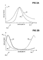
- FIG. 2A shows a graph 220 of a representative first-order green spectral response 226 and a representative green second-order spectral response 228, according to an embodiment of the invention.
- the y-axis 224 denotes reflectance as a function of wavelength on the x-axis 222.
- the second-order response 228 has a narrower spectral bandwidth and improved color saturation.
- the second-order response 228 can be utilized in one embodiment of the invention in lieu of the first-order response 226 for increased saturation and color component.
- the second-order response 228 is utilized for increased saturation
- the first-order response 226 is utilized for increased brightness and white level.
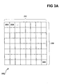
- FIG. 3A shows an array of passive pixel mechanisms 200, according to an embodiment of the invention.
- the passive pixel mechanisms 200 include the mechanisms 200A, 200B, ..., 200N, organized into columns 202 and rows 204.
- Each of the pixel mechanisms 200 is able to variably select a visible wavelength at an intensity by optical interference and absorption, in correspondence with a displayable image.
- the pixel mechanisms 200 can be considered the apparatus for performing this functionality in one embodiment of the invention.
- the mechanisms 200 are passive in that they do not generate light by themselves, but rather reflect or transmit ambient and/or supplemental light.
- each of the passive pixel mechanisms 200 includes one or more of the electronic device 100.
- a pixel may include one or more of the device 100.
- each of the mechanisms 200 may include only one electronic device 100, because the single device 100 is able to display substantially any color at any intensity.
- each of the mechanisms 200 may include three of the electronic devices 100, one for each of the red color component, the green color component, and the blue color component.
- a controller 302 controls the pixel mechanisms 200, effectively providing a pixilated displayable image to the pixel mechanisms 200. That is, in the embodiment where the mechanisms 200 each include one or more of the electronic device 100, the controller 302 changes the thickness 108 of the cavity 106 of each device 100, so that the image is properly rendered by the pixel mechanisms 200, for display to a user 308.
- the controller 302 thus electrically or otherwise adjusts the thickness 108 of the optical cavity 106, where, once adjusted, the thickness 108 is maintained by the flexure 110.
- the controller 302 may receive the displayable image from an image source 306 in a pixilated or a non-pixilated manner. If non-pixilated, or if pixilated in a manner that does not correspond on a one-to-one basis to the array of passive pixel mechanisms 200, the controller 302 itself divides the image into pixels corresponding to the array of passive pixel mechanisms 200.
- the image source 306 itself may be external to the display device 300, as in the embodiment of FIG. 3B, or internal thereto.
- the image source 306 may thus be a desktop computer external to the display device 300, or may be a laptop or notebook computer, personal digital assistant (PDA) device, wireless phone, or other device of which the display device 300 is a part.
- PDA personal digital assistant
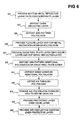
- FIG. 4 shows a method of use 400, according to an embodiment of the invention, for a display device, such as the display device 300 of FIG. 3B.
- a displayable image is divided into pixels (402), resulting in a pixilated displayable image.
- Light is optionally provided (404), to supplement any ambient light.
- a corresponding visible wavelength is selected, at a corresponding intensity, by optical interference and absorption (406), as has been described.
- the corresponding wavelength at the corresponding intensity may be selected in a digital or an analog manner, as has also been described.
- FIG. 5 shows a pair of electronic devices 500A and 500B for at least partially displaying a corresponding pair of pixels of a displayable image, according to an embodiment of the invention.
- Each of the electronic devices 500A and 500B is a specific embodiment of the electronic device 100 of FIG. 1A, and thus the description of FIG. 1A is equally applicable to FIG. 5 as well.
- the electronic devices 500A and 500B can each be used to realize each of the passive pixel mechanisms 200 of FIG. 3A, in one embodiment of the invention.
- the following description of FIG. 5 is made with specific reference to the electronic device 500A, but is identically applicable to the electronic device 500B.
- FIG. 5 is not drawn to scale, for illustrative clarity.
- FIG. 6 shows a method 600 for manufacturing an electronic device, such as the electronic device 500A or 500B of FIG. 5, or a display device having a number of such electronic devices, according to an embodiment of the invention.
- a bottom metal reflector layer is provided on a silicon substrate layer (602). This may include depositing and patterning the bottom metal reflector layer.
- the bottom metal reflector layer is the bottom reflector 104.
- an oxide dielectric layer is deposited (604), which in FIG. 5 is the thin dielectric 504.
- An oxide pixel plate layer is provided on the flexure layer and the top metal reflector layer (610). This can include depositing the oxide and patterning the oxide.
- the oxide pixel plate layer is the dielectric pixel plate 506.
- Additional polysilicon or additional filler material is then deposited on the oxide pixel plate layer and patterned (612), to act as a placeholder for an air cavity to be formed.
- the polysilicon thus occupies the space of the air cavity 514.
- An oxide layer is deposited on this polysilicon (614), which in FIG. 5 is the oxide 518 and 512.
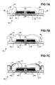
- FIGs. 7A and 7B shows the electronic device 100 of FIG. 1A, according to a specific embodiment of the invention.
- the description of FIG. 1A is thus applicable to FIGs. 7A and 7B as well.
- the electronic device 100 of the embodiment of FIGs. 7A and 7B is more generally a Fabry-Perot-based device.
- the sawing and packaging of optical micro-electrical mechanical system (MEMS) devices such as micro-mirrors, Fabry-Perot devices, and diffraction-based devices, can be difficult because of the fragility of the MEMS components, and the need for a transparent package.
- MEMS are generally semiconductor chips that have a top layer of mechanical devices, such as mirrors, fluid sensors, and so on.
- Wafer sawing is a wet process that can damage and/or contaminate the delicate devices upon release. Releasing the devices from sacrificial layers after sawing is difficult and costly if performed on a die-by-die basis. Packaging of such devices usually includes bonding a glass window to a package on a ceramic or other substrate, which can be costly, difficult to perform, and may add considerable size to the device.
- the electronic device 100 of the embodiment of FIGs. 7A and 7B overcomes these problems.
- a sacrificial material 704 is deposited over the movable components of the device 100, including the flexure 110, the reflective layers 102 and 104 that define the optical cavity 106, and the spring mechanism 112 that have been described.
- a layer 702 is deposited over and makes contact with this substrate at the locations indicated by the reference number 708. Openings 706 are patterned and etched in the layer 702.
- the device 100 is released by isotropically etching away the sacrificial material 704, using selective release chemistries known within the art, which may be dry or wet processes.
- the process described in relation to FIGs. 7A and 7B enables encapsulation within a clean-room environment without conventional packaging, such that the process may be described as self-packaging. Because the process is preferably performed in a clean-room environment, and the release operation occurs inside a protective cavity, increased yields can result. Once the cavities are sealed, the die can be sawed off, as known within the art, without damaging the device 100.
- FIG. 7C shows the electronic device 100 of FIG. 1A, according to another specific embodiment of the invention.
- the description of FIG. 1A is thus applicable to FIG. 7C as well.
- the non-active area includes the space between pixels, support posts, the flexure area, and so on. Light reflected from the non-active area can increase the black state reflectance, reducing overall system contrast.
- the electronic device 100 of the embodiment of FIG. 7C reduces this effect by including an absorbing layer, or border mask, 722 to cover such non-active areas.
- the self-packaging material 710 that has been described in conjunction with FIG. 7B provides a substrate for the border mask 722.
- Other like-numbered components of FIG. 7C relative to FIGs. 7A and 7B are identical to their counterparts of FIGs. 7A and 7B, and are not re-described in relation to FIG. 7C.
- the border mask 722 may be composed of a variety of different materials, including absorptive polymers, photo-imageable absorptive polymers, metal and/or dielectric composites, and/or interference-based induced absorbers. Absorptive polymers are typically spun on and imaged with a photoresist mask and develop process. Photo-imageable polymers can be patterned directly with lithographic techniques known within the art. Metal and/or dielectric composites known as cermets are other materials that can be used, and have typically been developed for use as solar absorbers. Such materials include black molybdenum, black tungsten, and black chrome, and have very high absorbance. Further, they can be deposited with sputtering or evaporation techniques known within the art. Induced absorbers maximize the absorbance within a dissipating layer, by tuning layer thickness. Induced absorbers are relatively thin, such as less than 1000 ⁇ .
- the electronic device 100 of the embodiment of FIG. 7C lends itself to a three-state operation having dedicated pixel types. For instance, there may be a type-one three-state pixel, having the color states red, green, and black, or there may be a type-two three-state pixel, having the color states red, blue, and black. There may also be a type-three three-state pixel, having the color states green, blue, and black.
- the configuration of this operation includes groups of three-state pixels. Different pixels in the group are designed to operate with different states. The different color states are controlled by the thickness of the sacrificial material 704.
- Such a configuration can be operated in a digital mode, with one pixel plate, or reflector, state in a non-contact position, and the other two states in contact with either the top or bottom capacitor plates, or reflectors.
- This has the advantage over a single-gap, two-state, configuration by allowing a color to be produced by two of the three pixels, instead of one of the three pixels, leading to brighter colors.
- the electronic device 100 of the embodiment of FIG. 7C also lends itself a dual-gap, dual-capacitor pixel design, which is characterized by the reflector 102 moving forming two variable capacitors, as is now described.
- a layer 720 is a partial reflector on the underside of the layer 702, and is over the reflector 102.
- the layer 720 acts as both a partial reflector and as a capacitor plate.
- the reflector 102 may be driven up towards the layer 720, or down towards reflector, or capacitor plate, 104 electrostatically.
- the spring mechanism 112 thus is deflected in two directions, and needs to travel only about half as far from its equilibrium position to cover the same total travel as when deflected in just one direction. This increased travel range enables modes of operation where pixels can produce multiple colors, multiple saturations, and black.
- the cavity made by removing the sacrificial material 106 serves as one gap, and the optical cavity 704 serves as another gap in this design.
- the electronic device 100 of any of the embodiments of FIGs. 7A, 7B, and 7C lends itself to single-gap, dual-mode (or, multi-level) operation, where the modes include contact between the reflectors 102 and 104, and non-contact between the reflectors 102 and 104.
- Each pixel is capable of creating multiple colors and intensities as needed for color displays. The pixels operate in a contact mode at one gap extreme, and in a non-contact mode for the remaining states.
- the pixel gap which is the thickness 108 of FIG. 1A that has been described, in a non-contact mode, such as an analog mode, a multi-level digital mode, or a combination analog and digital mode.
- the device 100 may need the thickness 108 to be less than 1000 ⁇ to create black, about 1800 ⁇ to create blue, and about 2800 ⁇ to create red.
- a single-gap, voltage control mode of operation that can be utilized is to operate in a non-contact mode between red and blue, and then allow the pixel to snap to the black state in a digital mode.
- FIGs. 8A and 8B show a pair of electronic devices 800A and 800B for at least partially displaying a corresponding pair of pixels of a displayable image, according to varying embodiment of the invention.
- Each of the electronic devices 800A and 800B is a specific embodiment of the electronic device 100 of FIG. 1A, and thus the description of FIG. 1A is equally applicable to FIGs. 8A and 8B as well. It is noted that as pixel size is reduced, a smaller aperture ratio usually results.
- Like-numbered components of FIGs. 8A and 8B relative to FIGs. 1A and 7A-7C are identical, and are not otherwise described with respect to FIGs. 8A and 8B. Further, for illustrative clarity only, not all components of FIGs. 1A and 7A-7C are shown in FIGs. 8A and 8B.
- the disadvantage of reduced aperture ratio is overcome by the electronic devices 800A and 800B by employing integral lenses 804A and 804B applied directly to the monolithic MEMS devices 800A and 800B, using coating or depositional techniques.
- the self-packaging layer 702 provides a substrate for these micro-lenses 804A and 804B, after an initial layer 802 has been deposited.
- the lenses 804A and 804B can be formed by patterning photoresist or other photo-imageable polymer using known lithographic techniques, and then partially flowing the patterns to the desired lens profile with heat treatment. The polymer may remain as the final lenses, or can be used as a mask to transfer the lens pattern to the underlying layer 802 with plasma or reactive-ion etching.
- the lenses 804A and 804B can be made more efficient by matching the shape thereof to the underlying pixels.
- anti-stiction bumps are placed on the bottom reflector 104 prior to fabrication of the top reflector 102.
- FIGS. 10A, 10B, and 10C illustratively depict the manner by which anti-stiction bumps can be fabricated on the bottom reflector 104, according to another embodiment of the invention.
- the flexure 110 and the bottom reflector 104 of the electronic device 100 are already present, as before.
- a first sacrificial material 910 is deposited that has the same thickness of the desired anti-stiction bump height.
- the material 910 is patterned and etched to yield the recesses 912.
- a second sacrificial material 914 is deposited to achieve the total sacrificial layer thickness.
- subsequent layers such as the layer 916, are deposited into the recessions 912 to yield bumps 918 within the recessions 912.
Landscapes
- Physics & Mathematics (AREA)
- Engineering & Computer Science (AREA)
- General Physics & Mathematics (AREA)
- Computer Hardware Design (AREA)
- Theoretical Computer Science (AREA)
- Spectroscopy & Molecular Physics (AREA)
- Optics & Photonics (AREA)
- Mechanical Light Control Or Optical Switches (AREA)
- Electrochromic Elements, Electrophoresis, Or Variable Reflection Or Absorption Elements (AREA)
Applications Claiming Priority (2)
| Application Number | Priority Date | Filing Date | Title |
|---|---|---|---|
| US10/428,261 US7072093B2 (en) | 2003-04-30 | 2003-04-30 | Optical interference pixel display with charge control |
| US428261 | 2003-04-30 |
Publications (2)
| Publication Number | Publication Date |
|---|---|
| EP1473581A2 true EP1473581A2 (fr) | 2004-11-03 |
| EP1473581A3 EP1473581A3 (fr) | 2006-03-22 |
Family
ID=32990474
Family Applications (1)
| Application Number | Title | Priority Date | Filing Date |
|---|---|---|---|
| EP03024950A Withdrawn EP1473581A3 (fr) | 2003-04-30 | 2003-10-29 | Dispositif d'affichage par pixel à interférence optique avec contrôle de charge |
Country Status (4)
| Country | Link |
|---|---|
| US (2) | US7072093B2 (fr) |
| EP (1) | EP1473581A3 (fr) |
| JP (1) | JP2004334201A (fr) |
| TW (1) | TWI265313B (fr) |
Cited By (58)
| Publication number | Priority date | Publication date | Assignee | Title |
|---|---|---|---|---|
| WO2005073950A1 (fr) * | 2004-01-22 | 2005-08-11 | Hewlett-Packard Development Company, L.P. | Circuit de commande de charge |
| WO2006036365A1 (fr) * | 2004-09-15 | 2006-04-06 | Hewlett-Packard Development Company, L.P. | Projecteur a modulateur intensite-couleur |
| WO2006062600A1 (fr) * | 2004-12-07 | 2006-06-15 | Hewlett-Packard Development Company, L.P. | Modulateur de lumiere |
| US7172915B2 (en) | 2003-01-29 | 2007-02-06 | Qualcomm Mems Technologies Co., Ltd. | Optical-interference type display panel and method for making the same |
| WO2007040762A1 (fr) * | 2005-09-21 | 2007-04-12 | Hewlett-Packard Development Company, L.P. | Modulateur de lumiere a etat optique reglable |
| WO2007040756A1 (fr) * | 2005-10-03 | 2007-04-12 | Hewlett-Packard Development Company, L.P. | Circuit de commande pour eliminer la friction statique |
| US7236284B2 (en) | 1995-05-01 | 2007-06-26 | Idc, Llc | Photonic MEMS and structures |
| US7259449B2 (en) | 2004-09-27 | 2007-08-21 | Idc, Llc | Method and system for sealing a substrate |
| US7289259B2 (en) | 2004-09-27 | 2007-10-30 | Idc, Llc | Conductive bus structure for interferometric modulator array |
| US7302157B2 (en) | 2004-09-27 | 2007-11-27 | Idc, Llc | System and method for multi-level brightness in interferometric modulation |
| US7304784B2 (en) | 2004-09-27 | 2007-12-04 | Idc, Llc | Reflective display device having viewable display on both sides |
| WO2007120695A3 (fr) * | 2006-04-10 | 2007-12-27 | Hewlett Packard Development Co | Procédé et appareil de traitement d'images couleur riches |
| US7321456B2 (en) | 2004-09-27 | 2008-01-22 | Idc, Llc | Method and device for corner interferometric modulation |
| WO2007094875A3 (fr) * | 2005-11-21 | 2008-01-31 | Hewlett Packard Development Co | Absorbeurs de lumière et procédés |
| US7327510B2 (en) | 2004-09-27 | 2008-02-05 | Idc, Llc | Process for modifying offset voltage characteristics of an interferometric modulator |
| WO2007142978A3 (fr) * | 2006-06-01 | 2008-03-20 | Light Resonance Technologies L | Filtre/modulateur de lumière et ensemble de filtres/modulateurs |
| US7372613B2 (en) | 2004-09-27 | 2008-05-13 | Idc, Llc | Method and device for multistate interferometric light modulation |
| US7372619B2 (en) | 1994-05-05 | 2008-05-13 | Idc, Llc | Display device having a movable structure for modulating light and method thereof |
| US7385744B2 (en) | 2006-06-28 | 2008-06-10 | Qualcomm Mems Technologies, Inc. | Support structure for free-standing MEMS device and methods for forming the same |
| US7420725B2 (en) | 2004-09-27 | 2008-09-02 | Idc, Llc | Device having a conductive light absorbing mask and method for fabricating same |
| WO2007106697A3 (fr) * | 2006-03-09 | 2008-09-04 | Hewlett Packard Development Co | Element composite d'interferometre de fabry-perot et procede correspondant |
| US7460292B2 (en) | 2005-06-03 | 2008-12-02 | Qualcomm Mems Technologies, Inc. | Interferometric modulator with internal polarization and drive method |
| US7471442B2 (en) | 2006-06-15 | 2008-12-30 | Qualcomm Mems Technologies, Inc. | Method and apparatus for low range bit depth enhancements for MEMS display architectures |
| US7476327B2 (en) | 2004-05-04 | 2009-01-13 | Idc, Llc | Method of manufacture for microelectromechanical devices |
| US7527998B2 (en) | 2006-06-30 | 2009-05-05 | Qualcomm Mems Technologies, Inc. | Method of manufacturing MEMS devices providing air gap control |
| US7527995B2 (en) | 2004-09-27 | 2009-05-05 | Qualcomm Mems Technologies, Inc. | Method of making prestructure for MEMS systems |
| US7532377B2 (en) | 1998-04-08 | 2009-05-12 | Idc, Llc | Movable micro-electromechanical device |
| US7550810B2 (en) | 2006-02-23 | 2009-06-23 | Qualcomm Mems Technologies, Inc. | MEMS device having a layer movable at asymmetric rates |
| US7554714B2 (en) | 2004-09-27 | 2009-06-30 | Idc, Llc | Device and method for manipulation of thermal response in a modulator |
| US7554711B2 (en) | 1998-04-08 | 2009-06-30 | Idc, Llc. | MEMS devices with stiction bumps |
| US7564612B2 (en) | 2004-09-27 | 2009-07-21 | Idc, Llc | Photonic MEMS and structures |
| US7567373B2 (en) | 2004-07-29 | 2009-07-28 | Idc, Llc | System and method for micro-electromechanical operation of an interferometric modulator |
| US7587104B2 (en) | 2004-09-27 | 2009-09-08 | Idc, Llc | MEMS device fabricated on a pre-patterned substrate |
| US7612933B2 (en) | 2008-03-27 | 2009-11-03 | Qualcomm Mems Technologies, Inc. | Microelectromechanical device with spacing layer |
| US7629197B2 (en) | 2006-10-18 | 2009-12-08 | Qualcomm Mems Technologies, Inc. | Spatial light modulator |
| US7630119B2 (en) | 2004-09-27 | 2009-12-08 | Qualcomm Mems Technologies, Inc. | Apparatus and method for reducing slippage between structures in an interferometric modulator |
| US7630121B2 (en) | 2007-07-02 | 2009-12-08 | Qualcomm Mems Technologies, Inc. | Electromechanical device with optical function separated from mechanical and electrical function |
| US7643199B2 (en) | 2007-06-19 | 2010-01-05 | Qualcomm Mems Technologies, Inc. | High aperture-ratio top-reflective AM-iMod displays |
| US7643202B2 (en) | 2007-05-09 | 2010-01-05 | Qualcomm Mems Technologies, Inc. | Microelectromechanical system having a dielectric movable membrane and a mirror |
| US7649671B2 (en) | 2006-06-01 | 2010-01-19 | Qualcomm Mems Technologies, Inc. | Analog interferometric modulator device with electrostatic actuation and release |
| US7719752B2 (en) | 2007-05-11 | 2010-05-18 | Qualcomm Mems Technologies, Inc. | MEMS structures, methods of fabricating MEMS components on separate substrates and assembly of same |
| US7719500B2 (en) | 2004-09-27 | 2010-05-18 | Qualcomm Mems Technologies, Inc. | Reflective display pixels arranged in non-rectangular arrays |
| US7835061B2 (en) | 2006-06-28 | 2010-11-16 | Qualcomm Mems Technologies, Inc. | Support structures for free-standing electromechanical devices |
| US7893919B2 (en) | 2004-09-27 | 2011-02-22 | Qualcomm Mems Technologies, Inc. | Display region architectures |
| US7916980B2 (en) | 2006-01-13 | 2011-03-29 | Qualcomm Mems Technologies, Inc. | Interconnect structure for MEMS device |
| US7936497B2 (en) | 2004-09-27 | 2011-05-03 | Qualcomm Mems Technologies, Inc. | MEMS device having deformable membrane characterized by mechanical persistence |
| US7951634B2 (en) | 2004-09-27 | 2011-05-31 | Qualcomm Mems Technologies, Inc. | Method and device for protecting interferometric modulators from electrostatic discharge |
| US8008736B2 (en) | 2004-09-27 | 2011-08-30 | Qualcomm Mems Technologies, Inc. | Analog interferometric modulator device |
| US8072402B2 (en) | 2007-08-29 | 2011-12-06 | Qualcomm Mems Technologies, Inc. | Interferometric optical modulator with broadband reflection characteristics |
| US8358266B2 (en) | 2008-09-02 | 2013-01-22 | Qualcomm Mems Technologies, Inc. | Light turning device with prismatic light turning features |
| US8488228B2 (en) | 2009-09-28 | 2013-07-16 | Qualcomm Mems Technologies, Inc. | Interferometric display with interferometric reflector |
| US8736939B2 (en) | 2011-11-04 | 2014-05-27 | Qualcomm Mems Technologies, Inc. | Matching layer thin-films for an electromechanical systems reflective display device |
| US8736949B2 (en) | 2007-07-31 | 2014-05-27 | Qualcomm Mems Technologies, Inc. | Devices and methods for enhancing color shift of interferometric modulators |
| US8797628B2 (en) | 2007-10-19 | 2014-08-05 | Qualcomm Memstechnologies, Inc. | Display with integrated photovoltaic device |
| US8885244B2 (en) | 2004-09-27 | 2014-11-11 | Qualcomm Mems Technologies, Inc. | Display device |
| US8979349B2 (en) | 2009-05-29 | 2015-03-17 | Qualcomm Mems Technologies, Inc. | Illumination devices and methods of fabrication thereof |
| US9057872B2 (en) | 2010-08-31 | 2015-06-16 | Qualcomm Mems Technologies, Inc. | Dielectric enhanced mirror for IMOD display |
| CN105093518A (zh) * | 2010-08-20 | 2015-11-25 | 精工爱普生株式会社 | 滤光器、滤光器模块、光谱测量仪及光设备 |
Families Citing this family (236)
| Publication number | Priority date | Publication date | Assignee | Title |
|---|---|---|---|---|
| US6674562B1 (en) | 1994-05-05 | 2004-01-06 | Iridigm Display Corporation | Interferometric modulation of radiation |
| US6680792B2 (en) | 1994-05-05 | 2004-01-20 | Iridigm Display Corporation | Interferometric modulation of radiation |
| US7550794B2 (en) | 2002-09-20 | 2009-06-23 | Idc, Llc | Micromechanical systems device comprising a displaceable electrode and a charge-trapping layer |
| US7297471B1 (en) | 2003-04-15 | 2007-11-20 | Idc, Llc | Method for manufacturing an array of interferometric modulators |
| US7138984B1 (en) | 2001-06-05 | 2006-11-21 | Idc, Llc | Directly laminated touch sensitive screen |
| US7460291B2 (en) | 1994-05-05 | 2008-12-02 | Idc, Llc | Separable modulator |
| US8014059B2 (en) | 1994-05-05 | 2011-09-06 | Qualcomm Mems Technologies, Inc. | System and method for charge control in a MEMS device |
| US7471444B2 (en) | 1996-12-19 | 2008-12-30 | Idc, Llc | Interferometric modulation of radiation |
| US6794119B2 (en) | 2002-02-12 | 2004-09-21 | Iridigm Display Corporation | Method for fabricating a structure for a microelectromechanical systems (MEMS) device |
| US7781850B2 (en) | 2002-09-20 | 2010-08-24 | Qualcomm Mems Technologies, Inc. | Controlling electromechanical behavior of structures within a microelectromechanical systems device |
| US7370185B2 (en) * | 2003-04-30 | 2008-05-06 | Hewlett-Packard Development Company, L.P. | Self-packaged optical interference display device having anti-stiction bumps, integral micro-lens, and reflection-absorbing layers |
| TWI289708B (en) | 2002-12-25 | 2007-11-11 | Qualcomm Mems Technologies Inc | Optical interference type color display |
| TW594360B (en) | 2003-04-21 | 2004-06-21 | Prime View Int Corp Ltd | A method for fabricating an interference display cell |
| TWI224235B (en) * | 2003-04-21 | 2004-11-21 | Prime View Int Co Ltd | A method for fabricating an interference display cell |
| US6829132B2 (en) * | 2003-04-30 | 2004-12-07 | Hewlett-Packard Development Company, L.P. | Charge control of micro-electromechanical device |
| US7447891B2 (en) * | 2003-04-30 | 2008-11-04 | Hewlett-Packard Development Company, L.P. | Light modulator with concentric control-electrode structure |
| TW570896B (en) | 2003-05-26 | 2004-01-11 | Prime View Int Co Ltd | A method for fabricating an interference display cell |
| US7388247B1 (en) | 2003-05-28 | 2008-06-17 | The United States Of America As Represented By The Secretary Of The Navy | High precision microelectromechanical capacitor with programmable voltage source |
| US7221495B2 (en) | 2003-06-24 | 2007-05-22 | Idc Llc | Thin film precursor stack for MEMS manufacturing |
| TWI251712B (en) | 2003-08-15 | 2006-03-21 | Prime View Int Corp Ltd | Interference display plate |
| TW593127B (en) | 2003-08-18 | 2004-06-21 | Prime View Int Co Ltd | Interference display plate and manufacturing method thereof |
| TWI231865B (en) | 2003-08-26 | 2005-05-01 | Prime View Int Co Ltd | An interference display cell and fabrication method thereof |
| TW593126B (en) | 2003-09-30 | 2004-06-21 | Prime View Int Co Ltd | A structure of a micro electro mechanical system and manufacturing the same |
| US7012726B1 (en) | 2003-11-03 | 2006-03-14 | Idc, Llc | MEMS devices with unreleased thin film components |
| US7161728B2 (en) | 2003-12-09 | 2007-01-09 | Idc, Llc | Area array modulation and lead reduction in interferometric modulators |
| US7142346B2 (en) | 2003-12-09 | 2006-11-28 | Idc, Llc | System and method for addressing a MEMS display |
| US7532194B2 (en) | 2004-02-03 | 2009-05-12 | Idc, Llc | Driver voltage adjuster |
| US7342705B2 (en) | 2004-02-03 | 2008-03-11 | Idc, Llc | Spatial light modulator with integrated optical compensation structure |
| US7471443B2 (en) * | 2004-03-02 | 2008-12-30 | Hewlett-Packard Development Company, L.P. | Piezoelectric flexures for light modulator |
| US7119945B2 (en) | 2004-03-03 | 2006-10-10 | Idc, Llc | Altering temporal response of microelectromechanical elements |
| US7706050B2 (en) | 2004-03-05 | 2010-04-27 | Qualcomm Mems Technologies, Inc. | Integrated modulator illumination |
| US7855824B2 (en) | 2004-03-06 | 2010-12-21 | Qualcomm Mems Technologies, Inc. | Method and system for color optimization in a display |
| US7060895B2 (en) | 2004-05-04 | 2006-06-13 | Idc, Llc | Modifying the electro-mechanical behavior of devices |
| US7164520B2 (en) | 2004-05-12 | 2007-01-16 | Idc, Llc | Packaging for an interferometric modulator |
| US7256922B2 (en) | 2004-07-02 | 2007-08-14 | Idc, Llc | Interferometric modulators with thin film transistors |
| US7436389B2 (en) * | 2004-07-29 | 2008-10-14 | Eugene J Mar | Method and system for controlling the output of a diffractive light device |
| US7515147B2 (en) | 2004-08-27 | 2009-04-07 | Idc, Llc | Staggered column drive circuit systems and methods |
| US7560299B2 (en) * | 2004-08-27 | 2009-07-14 | Idc, Llc | Systems and methods of actuating MEMS display elements |
| US7499208B2 (en) | 2004-08-27 | 2009-03-03 | Udc, Llc | Current mode display driver circuit realization feature |
| US7551159B2 (en) | 2004-08-27 | 2009-06-23 | Idc, Llc | System and method of sensing actuation and release voltages of an interferometric modulator |
| US7889163B2 (en) * | 2004-08-27 | 2011-02-15 | Qualcomm Mems Technologies, Inc. | Drive method for MEMS devices |
| US7602375B2 (en) | 2004-09-27 | 2009-10-13 | Idc, Llc | Method and system for writing data to MEMS display elements |
| US7898521B2 (en) * | 2004-09-27 | 2011-03-01 | Qualcomm Mems Technologies, Inc. | Device and method for wavelength filtering |
| US7289256B2 (en) | 2004-09-27 | 2007-10-30 | Idc, Llc | Electrical characterization of interferometric modulators |
| US7573547B2 (en) * | 2004-09-27 | 2009-08-11 | Idc, Llc | System and method for protecting micro-structure of display array using spacers in gap within display device |
| US7369296B2 (en) | 2004-09-27 | 2008-05-06 | Idc, Llc | Device and method for modifying actuation voltage thresholds of a deformable membrane in an interferometric modulator |
| US8514169B2 (en) | 2004-09-27 | 2013-08-20 | Qualcomm Mems Technologies, Inc. | Apparatus and system for writing data to electromechanical display elements |
| US7916103B2 (en) | 2004-09-27 | 2011-03-29 | Qualcomm Mems Technologies, Inc. | System and method for display device with end-of-life phenomena |
| US20060076634A1 (en) | 2004-09-27 | 2006-04-13 | Lauren Palmateer | Method and system for packaging MEMS devices with incorporated getter |
| US7299681B2 (en) | 2004-09-27 | 2007-11-27 | Idc, Llc | Method and system for detecting leak in electronic devices |
| US7692839B2 (en) | 2004-09-27 | 2010-04-06 | Qualcomm Mems Technologies, Inc. | System and method of providing MEMS device with anti-stiction coating |
| US7653371B2 (en) | 2004-09-27 | 2010-01-26 | Qualcomm Mems Technologies, Inc. | Selectable capacitance circuit |
| US7710629B2 (en) | 2004-09-27 | 2010-05-04 | Qualcomm Mems Technologies, Inc. | System and method for display device with reinforcing substance |
| US7525730B2 (en) * | 2004-09-27 | 2009-04-28 | Idc, Llc | Method and device for generating white in an interferometric modulator display |
| US7586484B2 (en) | 2004-09-27 | 2009-09-08 | Idc, Llc | Controller and driver features for bi-stable display |
| US7446926B2 (en) | 2004-09-27 | 2008-11-04 | Idc, Llc | System and method of providing a regenerating protective coating in a MEMS device |
| US7750886B2 (en) | 2004-09-27 | 2010-07-06 | Qualcomm Mems Technologies, Inc. | Methods and devices for lighting displays |
| US7417783B2 (en) | 2004-09-27 | 2008-08-26 | Idc, Llc | Mirror and mirror layer for optical modulator and method |
| US7415186B2 (en) | 2004-09-27 | 2008-08-19 | Idc, Llc | Methods for visually inspecting interferometric modulators for defects |
| US7420728B2 (en) | 2004-09-27 | 2008-09-02 | Idc, Llc | Methods of fabricating interferometric modulators by selectively removing a material |
| US7136213B2 (en) | 2004-09-27 | 2006-11-14 | Idc, Llc | Interferometric modulators having charge persistence |
| US7184202B2 (en) | 2004-09-27 | 2007-02-27 | Idc, Llc | Method and system for packaging a MEMS device |
| US20060176487A1 (en) | 2004-09-27 | 2006-08-10 | William Cummings | Process control monitors for interferometric modulators |
| US7553684B2 (en) | 2004-09-27 | 2009-06-30 | Idc, Llc | Method of fabricating interferometric devices using lift-off processing techniques |
| US7928928B2 (en) | 2004-09-27 | 2011-04-19 | Qualcomm Mems Technologies, Inc. | Apparatus and method for reducing perceived color shift |
| US7349136B2 (en) | 2004-09-27 | 2008-03-25 | Idc, Llc | Method and device for a display having transparent components integrated therein |
| US7424198B2 (en) * | 2004-09-27 | 2008-09-09 | Idc, Llc | Method and device for packaging a substrate |
| US7368803B2 (en) | 2004-09-27 | 2008-05-06 | Idc, Llc | System and method for protecting microelectromechanical systems array using back-plate with non-flat portion |
| US7460246B2 (en) | 2004-09-27 | 2008-12-02 | Idc, Llc | Method and system for sensing light using interferometric elements |
| US7446927B2 (en) | 2004-09-27 | 2008-11-04 | Idc, Llc | MEMS switch with set and latch electrodes |
| US7492502B2 (en) | 2004-09-27 | 2009-02-17 | Idc, Llc | Method of fabricating a free-standing microstructure |
| US7345805B2 (en) | 2004-09-27 | 2008-03-18 | Idc, Llc | Interferometric modulator array with integrated MEMS electrical switches |
| US7724993B2 (en) | 2004-09-27 | 2010-05-25 | Qualcomm Mems Technologies, Inc. | MEMS switches with deforming membranes |
| US8102407B2 (en) | 2004-09-27 | 2012-01-24 | Qualcomm Mems Technologies, Inc. | Method and device for manipulating color in a display |
| US7161730B2 (en) | 2004-09-27 | 2007-01-09 | Idc, Llc | System and method for providing thermal compensation for an interferometric modulator display |
| US7701631B2 (en) | 2004-09-27 | 2010-04-20 | Qualcomm Mems Technologies, Inc. | Device having patterned spacers for backplates and method of making the same |
| US7944599B2 (en) | 2004-09-27 | 2011-05-17 | Qualcomm Mems Technologies, Inc. | Electromechanical device with optical function separated from mechanical and electrical function |
| US7813026B2 (en) | 2004-09-27 | 2010-10-12 | Qualcomm Mems Technologies, Inc. | System and method of reducing color shift in a display |
| US7920135B2 (en) | 2004-09-27 | 2011-04-05 | Qualcomm Mems Technologies, Inc. | Method and system for driving a bi-stable display |
| US7710636B2 (en) * | 2004-09-27 | 2010-05-04 | Qualcomm Mems Technologies, Inc. | Systems and methods using interferometric optical modulators and diffusers |
| US7369294B2 (en) | 2004-09-27 | 2008-05-06 | Idc, Llc | Ornamental display device |
| US7679627B2 (en) | 2004-09-27 | 2010-03-16 | Qualcomm Mems Technologies, Inc. | Controller and driver features for bi-stable display |
| US8310441B2 (en) | 2004-09-27 | 2012-11-13 | Qualcomm Mems Technologies, Inc. | Method and system for writing data to MEMS display elements |
| US7807488B2 (en) * | 2004-09-27 | 2010-10-05 | Qualcomm Mems Technologies, Inc. | Display element having filter material diffused in a substrate of the display element |
| US7612932B2 (en) | 2004-09-27 | 2009-11-03 | Idc, Llc | Microelectromechanical device with optical function separated from mechanical and electrical function |
| US7349141B2 (en) | 2004-09-27 | 2008-03-25 | Idc, Llc | Method and post structures for interferometric modulation |
| US7310179B2 (en) | 2004-09-27 | 2007-12-18 | Idc, Llc | Method and device for selective adjustment of hysteresis window |
| US7359066B2 (en) | 2004-09-27 | 2008-04-15 | Idc, Llc | Electro-optical measurement of hysteresis in interferometric modulators |
| US7130104B2 (en) * | 2004-09-27 | 2006-10-31 | Idc, Llc | Methods and devices for inhibiting tilting of a mirror in an interferometric modulator |
| US7343080B2 (en) | 2004-09-27 | 2008-03-11 | Idc, Llc | System and method of testing humidity in a sealed MEMS device |
| US7532195B2 (en) | 2004-09-27 | 2009-05-12 | Idc, Llc | Method and system for reducing power consumption in a display |
| US7675669B2 (en) | 2004-09-27 | 2010-03-09 | Qualcomm Mems Technologies, Inc. | Method and system for driving interferometric modulators |
| US7535466B2 (en) | 2004-09-27 | 2009-05-19 | Idc, Llc | System with server based control of client device display features |
| US7545550B2 (en) | 2004-09-27 | 2009-06-09 | Idc, Llc | Systems and methods of actuating MEMS display elements |
| US7561323B2 (en) * | 2004-09-27 | 2009-07-14 | Idc, Llc | Optical films for directing light towards active areas of displays |
| US7355780B2 (en) | 2004-09-27 | 2008-04-08 | Idc, Llc | System and method of illuminating interferometric modulators using backlighting |
| US7843410B2 (en) | 2004-09-27 | 2010-11-30 | Qualcomm Mems Technologies, Inc. | Method and device for electrically programmable display |
| US8124434B2 (en) | 2004-09-27 | 2012-02-28 | Qualcomm Mems Technologies, Inc. | Method and system for packaging a display |
| US8878825B2 (en) | 2004-09-27 | 2014-11-04 | Qualcomm Mems Technologies, Inc. | System and method for providing a variable refresh rate of an interferometric modulator display |
| BRPI0509575A (pt) | 2004-09-27 | 2007-10-09 | Idc Llc | método e dispositivo para modulação de luz interferométrica de multi-estados |
| US8031133B2 (en) | 2004-09-27 | 2011-10-04 | Qualcomm Mems Technologies, Inc. | Method and device for manipulating color in a display |
| US7405924B2 (en) | 2004-09-27 | 2008-07-29 | Idc, Llc | System and method for protecting microelectromechanical systems array using structurally reinforced back-plate |
| US7911428B2 (en) | 2004-09-27 | 2011-03-22 | Qualcomm Mems Technologies, Inc. | Method and device for manipulating color in a display |
| US7808703B2 (en) | 2004-09-27 | 2010-10-05 | Qualcomm Mems Technologies, Inc. | System and method for implementation of interferometric modulator displays |
| US7417735B2 (en) | 2004-09-27 | 2008-08-26 | Idc, Llc | Systems and methods for measuring color and contrast in specular reflective devices |
| US7626581B2 (en) | 2004-09-27 | 2009-12-01 | Idc, Llc | Device and method for display memory using manipulation of mechanical response |
| US7710632B2 (en) | 2004-09-27 | 2010-05-04 | Qualcomm Mems Technologies, Inc. | Display device having an array of spatial light modulators with integrated color filters |
| US8362987B2 (en) | 2004-09-27 | 2013-01-29 | Qualcomm Mems Technologies, Inc. | Method and device for manipulating color in a display |
| US7508571B2 (en) | 2004-09-27 | 2009-03-24 | Idc, Llc | Optical films for controlling angular characteristics of displays |
| US7453579B2 (en) | 2004-09-27 | 2008-11-18 | Idc, Llc | Measurement of the dynamic characteristics of interferometric modulators |
| US7684104B2 (en) | 2004-09-27 | 2010-03-23 | Idc, Llc | MEMS using filler material and method |
| US7630123B2 (en) * | 2004-09-27 | 2009-12-08 | Qualcomm Mems Technologies, Inc. | Method and device for compensating for color shift as a function of angle of view |
| US7668415B2 (en) | 2004-09-27 | 2010-02-23 | Qualcomm Mems Technologies, Inc. | Method and device for providing electronic circuitry on a backplate |
| JP4606466B2 (ja) * | 2004-10-15 | 2011-01-05 | ヒューレット−パッカード デベロップメント カンパニー エル.ピー. | 微小電気機械素子のための電荷制御回路 |
| TW200628877A (en) | 2005-02-04 | 2006-08-16 | Prime View Int Co Ltd | Method of manufacturing optical interference type color display |
| US7019887B1 (en) | 2005-04-08 | 2006-03-28 | Hewlett-Packard Development Company, L.P. | Light modulator device |
| US20060245028A1 (en) * | 2005-04-15 | 2006-11-02 | Sriram Ramamoorthi | Light modulator device |
| US7920136B2 (en) | 2005-05-05 | 2011-04-05 | Qualcomm Mems Technologies, Inc. | System and method of driving a MEMS display device |
| US7948457B2 (en) | 2005-05-05 | 2011-05-24 | Qualcomm Mems Technologies, Inc. | Systems and methods of actuating MEMS display elements |
| CA2607807A1 (fr) | 2005-05-05 | 2006-11-16 | Qualcomm Incorporated | Circuit integre pilote dynamique et configuration de panneau afficheur |
| US7884989B2 (en) | 2005-05-27 | 2011-02-08 | Qualcomm Mems Technologies, Inc. | White interferometric modulators and methods for forming the same |
| JP2009503564A (ja) | 2005-07-22 | 2009-01-29 | クアルコム,インコーポレイテッド | Memsデバイスのための支持構造、およびその方法 |
| CA2616268A1 (fr) | 2005-07-22 | 2007-02-01 | Qualcomm Incorporated | Dispositifs de microsysteme electromecanique comportant des structures de support et leurs procedes de fabrication |
| US20070019274A1 (en) * | 2005-07-25 | 2007-01-25 | Scott Lerner | Double pass light modulator |
| US7355779B2 (en) | 2005-09-02 | 2008-04-08 | Idc, Llc | Method and system for driving MEMS display elements |
| US20070052671A1 (en) * | 2005-09-02 | 2007-03-08 | Hewlett-Packard Development Company Lp | Pixel element actuation |
| WO2007041302A2 (fr) | 2005-09-30 | 2007-04-12 | Qualcomm Mems Technologies, Inc. | Dispositif mems et plaques d'interconnexion associées |
| CN100468127C (zh) * | 2005-10-07 | 2009-03-11 | 鸿富锦精密工业(深圳)有限公司 | 投影显示装置 |
| US7630114B2 (en) | 2005-10-28 | 2009-12-08 | Idc, Llc | Diffusion barrier layer for MEMS devices |
| US7760197B2 (en) * | 2005-10-31 | 2010-07-20 | Hewlett-Packard Development Company, L.P. | Fabry-perot interferometric MEMS electromagnetic wave modulator with zero-electric field |
| US8391630B2 (en) | 2005-12-22 | 2013-03-05 | Qualcomm Mems Technologies, Inc. | System and method for power reduction when decompressing video streams for interferometric modulator displays |
| US7795061B2 (en) | 2005-12-29 | 2010-09-14 | Qualcomm Mems Technologies, Inc. | Method of creating MEMS device cavities by a non-etching process |
| US7561133B2 (en) * | 2005-12-29 | 2009-07-14 | Xerox Corporation | System and methods of device independent display using tunable individually-addressable fabry-perot membranes |
| US7636151B2 (en) | 2006-01-06 | 2009-12-22 | Qualcomm Mems Technologies, Inc. | System and method for providing residual stress test structures |
| US7382515B2 (en) | 2006-01-18 | 2008-06-03 | Qualcomm Mems Technologies, Inc. | Silicon-rich silicon nitrides as etch stops in MEMS manufacture |
| US7652814B2 (en) | 2006-01-27 | 2010-01-26 | Qualcomm Mems Technologies, Inc. | MEMS device with integrated optical element |
| US8194056B2 (en) | 2006-02-09 | 2012-06-05 | Qualcomm Mems Technologies Inc. | Method and system for writing data to MEMS display elements |
| US7530696B2 (en) * | 2006-02-13 | 2009-05-12 | Hewlett-Packard Development Company, L.P. | Projectors and operation thereof |
| US7603001B2 (en) | 2006-02-17 | 2009-10-13 | Qualcomm Mems Technologies, Inc. | Method and apparatus for providing back-lighting in an interferometric modulator display device |
| US7582952B2 (en) | 2006-02-21 | 2009-09-01 | Qualcomm Mems Technologies, Inc. | Method for providing and removing discharging interconnect for chip-on-glass output leads and structures thereof |
| US7547568B2 (en) | 2006-02-22 | 2009-06-16 | Qualcomm Mems Technologies, Inc. | Electrical conditioning of MEMS device and insulating layer thereof |
| US7450295B2 (en) | 2006-03-02 | 2008-11-11 | Qualcomm Mems Technologies, Inc. | Methods for producing MEMS with protective coatings using multi-component sacrificial layers |
| US7643203B2 (en) * | 2006-04-10 | 2010-01-05 | Qualcomm Mems Technologies, Inc. | Interferometric optical display system with broadband characteristics |
| WO2007120887A2 (fr) | 2006-04-13 | 2007-10-25 | Qualcomm Mems Technologies, Inc | Encapsulation d'un dispositif mems à l'aide d'un cadre |
| US7903047B2 (en) | 2006-04-17 | 2011-03-08 | Qualcomm Mems Technologies, Inc. | Mode indicator for interferometric modulator displays |
| US7527996B2 (en) | 2006-04-19 | 2009-05-05 | Qualcomm Mems Technologies, Inc. | Non-planar surface structures and process for microelectromechanical systems |
| US7623287B2 (en) | 2006-04-19 | 2009-11-24 | Qualcomm Mems Technologies, Inc. | Non-planar surface structures and process for microelectromechanical systems |
| US7711239B2 (en) | 2006-04-19 | 2010-05-04 | Qualcomm Mems Technologies, Inc. | Microelectromechanical device and method utilizing nanoparticles |
| US7417784B2 (en) | 2006-04-19 | 2008-08-26 | Qualcomm Mems Technologies, Inc. | Microelectromechanical device and method utilizing a porous surface |
| US8004743B2 (en) | 2006-04-21 | 2011-08-23 | Qualcomm Mems Technologies, Inc. | Method and apparatus for providing brightness control in an interferometric modulator (IMOD) display |
| US8049713B2 (en) | 2006-04-24 | 2011-11-01 | Qualcomm Mems Technologies, Inc. | Power consumption optimized display update |
| US7369292B2 (en) | 2006-05-03 | 2008-05-06 | Qualcomm Mems Technologies, Inc. | Electrode and interconnect materials for MEMS devices |
| US7653267B2 (en) * | 2006-05-15 | 2010-01-26 | Newport Corporation | Electro-optic modulator with adjustable cavity size |
| US7405863B2 (en) | 2006-06-01 | 2008-07-29 | Qualcomm Mems Technologies, Inc. | Patterning of mechanical layer in MEMS to reduce stresses at supports |
| US7321457B2 (en) | 2006-06-01 | 2008-01-22 | Qualcomm Incorporated | Process and structure for fabrication of MEMS device having isolated edge posts |
| US7766498B2 (en) | 2006-06-21 | 2010-08-03 | Qualcomm Mems Technologies, Inc. | Linear solid state illuminator |
| US7702192B2 (en) | 2006-06-21 | 2010-04-20 | Qualcomm Mems Technologies, Inc. | Systems and methods for driving MEMS display |
| US7777715B2 (en) | 2006-06-29 | 2010-08-17 | Qualcomm Mems Technologies, Inc. | Passive circuits for de-multiplexing display inputs |
| US7388704B2 (en) | 2006-06-30 | 2008-06-17 | Qualcomm Mems Technologies, Inc. | Determination of interferometric modulator mirror curvature and airgap variation using digital photographs |
| US7566664B2 (en) | 2006-08-02 | 2009-07-28 | Qualcomm Mems Technologies, Inc. | Selective etching of MEMS using gaseous halides and reactive co-etchants |
| US7763546B2 (en) | 2006-08-02 | 2010-07-27 | Qualcomm Mems Technologies, Inc. | Methods for reducing surface charges during the manufacture of microelectromechanical systems devices |
| US7845841B2 (en) | 2006-08-28 | 2010-12-07 | Qualcomm Mems Technologies, Inc. | Angle sweeping holographic illuminator |
| WO2008045200A2 (fr) | 2006-10-06 | 2008-04-17 | Qualcomm Mems Technologies, Inc. | Structure d'affaiblissement optique intégrée dans un appareil d'éclairage |
| EP2069838A2 (fr) | 2006-10-06 | 2009-06-17 | Qualcomm Mems Technologies, Inc. | Dispositif d'éclairage intégrant un coupleur de lumière |
| WO2008045207A2 (fr) | 2006-10-06 | 2008-04-17 | Qualcomm Mems Technologies, Inc. | Guide de lumière |
| WO2008045462A2 (fr) | 2006-10-10 | 2008-04-17 | Qualcomm Mems Technologies, Inc. | Dispositif d'affichage à optiques diffractives |
| US7545552B2 (en) | 2006-10-19 | 2009-06-09 | Qualcomm Mems Technologies, Inc. | Sacrificial spacer process and resultant structure for MEMS support structure |
| US7864395B2 (en) | 2006-10-27 | 2011-01-04 | Qualcomm Mems Technologies, Inc. | Light guide including optical scattering elements and a method of manufacture |
| US7706042B2 (en) | 2006-12-20 | 2010-04-27 | Qualcomm Mems Technologies, Inc. | MEMS device and interconnects for same |
| US7777954B2 (en) | 2007-01-30 | 2010-08-17 | Qualcomm Mems Technologies, Inc. | Systems and methods of providing a light guiding layer |
| US8115987B2 (en) | 2007-02-01 | 2012-02-14 | Qualcomm Mems Technologies, Inc. | Modulating the intensity of light from an interferometric reflector |
| JP5492571B2 (ja) * | 2007-02-20 | 2014-05-14 | クォルコム・メムズ・テクノロジーズ・インコーポレーテッド | Memsのエッチングを行うための機器および方法 |
| US7916378B2 (en) * | 2007-03-08 | 2011-03-29 | Qualcomm Mems Technologies, Inc. | Method and apparatus for providing a light absorbing mask in an interferometric modulator display |
| US7742220B2 (en) | 2007-03-28 | 2010-06-22 | Qualcomm Mems Technologies, Inc. | Microelectromechanical device and method utilizing conducting layers separated by stops |
| US7715085B2 (en) | 2007-05-09 | 2010-05-11 | Qualcomm Mems Technologies, Inc. | Electromechanical system having a dielectric movable membrane and a mirror |
| US7782517B2 (en) | 2007-06-21 | 2010-08-24 | Qualcomm Mems Technologies, Inc. | Infrared and dual mode displays |
| TW200920685A (en) * | 2007-06-29 | 2009-05-16 | Qualcomm Mems Technologies Inc | Electromechanical device treatment with water vapor |
| KR101435527B1 (ko) * | 2007-07-25 | 2014-08-29 | 삼성디스플레이 주식회사 | 표시 장치 |
| US7570415B2 (en) | 2007-08-07 | 2009-08-04 | Qualcomm Mems Technologies, Inc. | MEMS device and interconnects for same |
| JP2011501874A (ja) | 2007-09-14 | 2011-01-13 | クォルコム・メムズ・テクノロジーズ・インコーポレーテッド | Mems製造において使用されるエッチングプロセス |
| US7773286B2 (en) | 2007-09-14 | 2010-08-10 | Qualcomm Mems Technologies, Inc. | Periodic dimple array |
| US7847999B2 (en) | 2007-09-14 | 2010-12-07 | Qualcomm Mems Technologies, Inc. | Interferometric modulator display devices |
| CN101802678B (zh) * | 2007-09-17 | 2014-03-12 | 高通Mems科技公司 | 半透明/透射反射型发光干涉式调制器装置 |
| US8058549B2 (en) | 2007-10-19 | 2011-11-15 | Qualcomm Mems Technologies, Inc. | Photovoltaic devices with integrated color interferometric film stacks |
| JP2011504243A (ja) | 2007-10-23 | 2011-02-03 | クォルコム・メムズ・テクノロジーズ・インコーポレーテッド | 調節可能透過型memsベースの装置 |
| US8941631B2 (en) | 2007-11-16 | 2015-01-27 | Qualcomm Mems Technologies, Inc. | Simultaneous light collection and illumination on an active display |
| US7715079B2 (en) | 2007-12-07 | 2010-05-11 | Qualcomm Mems Technologies, Inc. | MEMS devices requiring no mechanical support |
| US8068710B2 (en) | 2007-12-07 | 2011-11-29 | Qualcomm Mems Technologies, Inc. | Decoupled holographic film and diffuser |
| US7949213B2 (en) | 2007-12-07 | 2011-05-24 | Qualcomm Mems Technologies, Inc. | Light illumination of displays with front light guide and coupling elements |
| CN101897033B (zh) | 2007-12-17 | 2012-11-14 | 高通Mems科技公司 | 具有干涉式背面掩模的光伏装置及其制造方法 |
| WO2009102733A2 (fr) | 2008-02-12 | 2009-08-20 | Qualcomm Mems Technologies, Inc. | Diffuseur de lumiere avant integre pour afficheurs reflechissants |
| WO2009102731A2 (fr) | 2008-02-12 | 2009-08-20 | Qualcomm Mems Technologies, Inc. | Dispositifs et procédés permettant d'améliore la luminosité d'écrans utilisant des couches de conversion d'angle |
| US8164821B2 (en) | 2008-02-22 | 2012-04-24 | Qualcomm Mems Technologies, Inc. | Microelectromechanical device with thermal expansion balancing layer or stiffening layer |
| US7944604B2 (en) | 2008-03-07 | 2011-05-17 | Qualcomm Mems Technologies, Inc. | Interferometric modulator in transmission mode |
| US7948672B2 (en) * | 2008-03-07 | 2011-05-24 | Qualcomm Mems Technologies, Inc. | System and methods for tiling display panels |
| US7898723B2 (en) | 2008-04-02 | 2011-03-01 | Qualcomm Mems Technologies, Inc. | Microelectromechanical systems display element with photovoltaic structure |
| US7969638B2 (en) | 2008-04-10 | 2011-06-28 | Qualcomm Mems Technologies, Inc. | Device having thin black mask and method of fabricating the same |
| WO2009129264A1 (fr) | 2008-04-15 | 2009-10-22 | Qualcomm Mems Technologies, Inc. | Lumière ayant une propagation bidirectionnelle |
| US8164588B2 (en) * | 2008-05-23 | 2012-04-24 | Teledyne Scientific & Imaging, Llc | System and method for MEMS array actuation including a charge integration circuit to modulate the charge on a variable gap capacitor during an actuation cycle |
| US7746539B2 (en) | 2008-06-25 | 2010-06-29 | Qualcomm Mems Technologies, Inc. | Method for packing a display device and the device obtained thereof |
| US7768690B2 (en) | 2008-06-25 | 2010-08-03 | Qualcomm Mems Technologies, Inc. | Backlight displays |
| US8023167B2 (en) | 2008-06-25 | 2011-09-20 | Qualcomm Mems Technologies, Inc. | Backlight displays |
| US7859740B2 (en) | 2008-07-11 | 2010-12-28 | Qualcomm Mems Technologies, Inc. | Stiction mitigation with integrated mech micro-cantilevers through vertical stress gradient control |
| US7855826B2 (en) | 2008-08-12 | 2010-12-21 | Qualcomm Mems Technologies, Inc. | Method and apparatus to reduce or eliminate stiction and image retention in interferometric modulator devices |
| US8172417B2 (en) | 2009-03-06 | 2012-05-08 | Qualcomm Mems Technologies, Inc. | Shaped frontlight reflector for use with display |
| US8270056B2 (en) | 2009-03-23 | 2012-09-18 | Qualcomm Mems Technologies, Inc. | Display device with openings between sub-pixels and method of making same |
| US8736590B2 (en) | 2009-03-27 | 2014-05-27 | Qualcomm Mems Technologies, Inc. | Low voltage driver scheme for interferometric modulators |
| US7864403B2 (en) | 2009-03-27 | 2011-01-04 | Qualcomm Mems Technologies, Inc. | Post-release adjustment of interferometric modulator reflectivity |
| US7990604B2 (en) | 2009-06-15 | 2011-08-02 | Qualcomm Mems Technologies, Inc. | Analog interferometric modulator |
| NO333724B1 (no) * | 2009-08-14 | 2013-09-02 | Sintef | En mikromekanisk rekke med optisk reflekterende overflater |
| US8270062B2 (en) | 2009-09-17 | 2012-09-18 | Qualcomm Mems Technologies, Inc. | Display device with at least one movable stop element |
| US7999995B2 (en) * | 2009-09-28 | 2011-08-16 | Sharp Laboratories Of America, Inc. | Full color range interferometric modulation |
| US8379392B2 (en) | 2009-10-23 | 2013-02-19 | Qualcomm Mems Technologies, Inc. | Light-based sealing and device packaging |
| EP2556403A1 (fr) | 2010-04-09 | 2013-02-13 | Qualcomm Mems Technologies, Inc. | Couche mécanique d'un dispositif électromécanique et ses procédés de formation |
| CA2796518A1 (fr) | 2010-04-16 | 2011-10-20 | Flex Lighting Ii, Llc | Enseigne comprenant un guide de lumiere base sur un film |
| JP2013525955A (ja) | 2010-04-16 | 2013-06-20 | フレックス ライティング 2,エルエルシー | フィルムベースのライトガイドを備える照明デバイス |
| US8848294B2 (en) | 2010-05-20 | 2014-09-30 | Qualcomm Mems Technologies, Inc. | Method and structure capable of changing color saturation |
| EP2606485A1 (fr) * | 2010-08-17 | 2013-06-26 | Qualcomm Mems Technologies, Inc. | Actionnement et étalonnage d'une électrode neutre de charge dans un dispositif d'affichage interférométrique |
| US8670171B2 (en) | 2010-10-18 | 2014-03-11 | Qualcomm Mems Technologies, Inc. | Display having an embedded microlens array |
| US8902484B2 (en) | 2010-12-15 | 2014-12-02 | Qualcomm Mems Technologies, Inc. | Holographic brightness enhancement film |
| US8963159B2 (en) | 2011-04-04 | 2015-02-24 | Qualcomm Mems Technologies, Inc. | Pixel via and methods of forming the same |
| US9134527B2 (en) | 2011-04-04 | 2015-09-15 | Qualcomm Mems Technologies, Inc. | Pixel via and methods of forming the same |
| US8659816B2 (en) | 2011-04-25 | 2014-02-25 | Qualcomm Mems Technologies, Inc. | Mechanical layer and methods of making the same |
| US9140900B2 (en) | 2011-07-20 | 2015-09-22 | Pixtronix, Inc. | Displays having self-aligned apertures and methods of making the same |
| TWI444587B (zh) | 2011-08-03 | 2014-07-11 | Nat Univ Tsing Hua | 零耗能遙測曲度感測結構及其方法 |
| US9373732B2 (en) | 2012-02-07 | 2016-06-21 | Semiconductor Components Industries, Llc | Image sensors with reflective optical cavity pixels |
| US9035934B2 (en) | 2012-05-02 | 2015-05-19 | Qualcomm Mems Technologies, Inc. | Voltage biased pull analog interferometric modulator with charge injection control |
| US9305497B2 (en) | 2012-08-31 | 2016-04-05 | Qualcomm Mems Technologies, Inc. | Systems, devices, and methods for driving an analog interferometric modulator |
| JP5987573B2 (ja) | 2012-09-12 | 2016-09-07 | セイコーエプソン株式会社 | 光学モジュール、電子機器、及び駆動方法 |
| US10325947B2 (en) | 2013-01-17 | 2019-06-18 | Semiconductor Components Industries, Llc | Global shutter image sensors with light guide and light shield structures |
| JP5999159B2 (ja) * | 2014-10-01 | 2016-09-28 | セイコーエプソン株式会社 | 光フィルター、光フィルターモジュール、分光測定器および光機器 |
| JP6720112B2 (ja) | 2017-05-23 | 2020-07-08 | 浜松ホトニクス株式会社 | フィルタ制御式導出方法、光計測システム、ファブリペロー干渉フィルタの制御方法、及び、フィルタ制御プログラム |
| DE102018217996A1 (de) * | 2018-10-22 | 2020-04-23 | Robert Bosch Gmbh | Interferometerelement, Spektrometer und Verfahren zum Betreiben eines Interferometers |
| US10962711B2 (en) * | 2018-11-29 | 2021-03-30 | Taiwan Semiconductor Manufacturing Company, Ltd. | Semiconductor package and manufacturing method thereof |
| JP7110081B2 (ja) | 2018-12-18 | 2022-08-01 | 浜松ホトニクス株式会社 | 制御装置、光学フィルタシステム、制御方法 |
| US12305980B2 (en) * | 2021-09-20 | 2025-05-20 | Zygo Corporation | Optical contact metrology |
Citations (4)
| Publication number | Priority date | Publication date | Assignee | Title |
|---|---|---|---|---|
| EP0695959A1 (fr) | 1994-07-29 | 1996-02-07 | AT&T Corp. | Dispositif d'affichage à vue directe basé sur des modulateurs micromécaniques |
| US5986796A (en) | 1993-03-17 | 1999-11-16 | Etalon Inc. | Visible spectrum modulator arrays |
| US20020015215A1 (en) * | 1994-05-05 | 2002-02-07 | Iridigm Display Corporation, A Delaware Corporation | Interferometric modulation of radiation |
| WO2002091059A1 (fr) | 2001-05-03 | 2002-11-14 | Nokia Corporation | Plaque d'epaisseur variable a mode de reglage electrique |
Family Cites Families (17)
| Publication number | Priority date | Publication date | Assignee | Title |
|---|---|---|---|---|
| GB2222923B (en) * | 1988-09-14 | 1992-09-23 | Marconi Gec Ltd | Display apparatus |
| US6392341B2 (en) * | 1993-07-20 | 2002-05-21 | University Of Georgia Research Foundation, Inc. | Resonant microcavity display with a light distribution element |
| US6680792B2 (en) * | 1994-05-05 | 2004-01-20 | Iridigm Display Corporation | Interferometric modulation of radiation |
| US7123216B1 (en) * | 1994-05-05 | 2006-10-17 | Idc, Llc | Photonic MEMS and structures |
| US6040937A (en) * | 1994-05-05 | 2000-03-21 | Etalon, Inc. | Interferometric modulation |
| US5771321A (en) | 1996-01-04 | 1998-06-23 | Massachusetts Institute Of Technology | Micromechanical optical switch and flat panel display |
| US6031653A (en) * | 1997-08-28 | 2000-02-29 | California Institute Of Technology | Low-cost thin-metal-film interference filters |
| US6297907B1 (en) * | 1997-09-02 | 2001-10-02 | California Institute Of Technology | Devices based on surface plasmon interference filters |
| US6154591A (en) * | 1998-04-20 | 2000-11-28 | British Telecommunications Public Limited Company | Tunable optical device |
| US6329974B1 (en) | 1998-04-30 | 2001-12-11 | Agilent Technologies, Inc. | Electro-optical material-based display device having analog pixel drivers |
| US6040936A (en) * | 1998-10-08 | 2000-03-21 | Nec Research Institute, Inc. | Optical transmission control apparatus utilizing metal films perforated with subwavelength-diameter holes |
| US6362018B1 (en) * | 2000-02-02 | 2002-03-26 | Motorola, Inc. | Method for fabricating MEMS variable capacitor with stabilized electrostatic drive |
| US6373632B1 (en) * | 2000-03-03 | 2002-04-16 | Axsun Technologies, Inc. | Tunable Fabry-Perot filter |
| US6384953B1 (en) * | 2000-06-29 | 2002-05-07 | The United States Of America As Represented By The Secretary Of The Navy | Micro-dynamic optical device |
| JP2004505444A (ja) | 2000-07-24 | 2004-02-19 | モトローラ・インコーポレイテッド | 薄膜金属酸化物構造体およびその製造方法 |
| US6467879B1 (en) | 2000-10-16 | 2002-10-22 | Xerox Corporation | Method and apparatus for preventing degradation of electrostatically actuated devices |
| US20020126864A1 (en) * | 2001-03-07 | 2002-09-12 | Dennis George J. | Hearing devices kit |
-
2003
- 2003-04-30 US US10/428,261 patent/US7072093B2/en not_active Expired - Fee Related
- 2003-10-28 TW TW092129957A patent/TWI265313B/zh not_active IP Right Cessation
- 2003-10-29 EP EP03024950A patent/EP1473581A3/fr not_active Withdrawn
-
2004
- 2004-04-27 JP JP2004131495A patent/JP2004334201A/ja active Pending
-
2005
- 2005-12-04 US US11/294,513 patent/US7221497B2/en not_active Expired - Lifetime
Patent Citations (4)
| Publication number | Priority date | Publication date | Assignee | Title |
|---|---|---|---|---|
| US5986796A (en) | 1993-03-17 | 1999-11-16 | Etalon Inc. | Visible spectrum modulator arrays |
| US20020015215A1 (en) * | 1994-05-05 | 2002-02-07 | Iridigm Display Corporation, A Delaware Corporation | Interferometric modulation of radiation |
| EP0695959A1 (fr) | 1994-07-29 | 1996-02-07 | AT&T Corp. | Dispositif d'affichage à vue directe basé sur des modulateurs micromécaniques |
| WO2002091059A1 (fr) | 2001-05-03 | 2002-11-14 | Nokia Corporation | Plaque d'epaisseur variable a mode de reglage electrique |
Cited By (79)
| Publication number | Priority date | Publication date | Assignee | Title |
|---|---|---|---|---|
| US7372619B2 (en) | 1994-05-05 | 2008-05-13 | Idc, Llc | Display device having a movable structure for modulating light and method thereof |
| US7236284B2 (en) | 1995-05-01 | 2007-06-26 | Idc, Llc | Photonic MEMS and structures |
| US7554711B2 (en) | 1998-04-08 | 2009-06-30 | Idc, Llc. | MEMS devices with stiction bumps |
| US7532377B2 (en) | 1998-04-08 | 2009-05-12 | Idc, Llc | Movable micro-electromechanical device |
| US7830586B2 (en) | 1999-10-05 | 2010-11-09 | Qualcomm Mems Technologies, Inc. | Transparent thin films |
| US7172915B2 (en) | 2003-01-29 | 2007-02-06 | Qualcomm Mems Technologies Co., Ltd. | Optical-interference type display panel and method for making the same |
| US7218499B2 (en) | 2003-05-14 | 2007-05-15 | Hewlett-Packard Development Company, L.P. | Charge control circuit |
| GB2427035A (en) * | 2004-01-22 | 2006-12-13 | Hewlett Packard Development Co | A Charge Control Circuit |
| WO2005073950A1 (fr) * | 2004-01-22 | 2005-08-11 | Hewlett-Packard Development Company, L.P. | Circuit de commande de charge |
| GB2427035B (en) * | 2004-01-22 | 2007-10-03 | Hewlett Packard Development Co | A Charge Control Circuit |
| US7476327B2 (en) | 2004-05-04 | 2009-01-13 | Idc, Llc | Method of manufacture for microelectromechanical devices |
| US7567373B2 (en) | 2004-07-29 | 2009-07-28 | Idc, Llc | System and method for micro-electromechanical operation of an interferometric modulator |
| GB2433788A (en) * | 2004-09-15 | 2007-07-04 | Hewlett Packard Development Co | Projector with intensity-colour modulator |
| WO2006036365A1 (fr) * | 2004-09-15 | 2006-04-06 | Hewlett-Packard Development Company, L.P. | Projecteur a modulateur intensite-couleur |
| US8008736B2 (en) | 2004-09-27 | 2011-08-30 | Qualcomm Mems Technologies, Inc. | Analog interferometric modulator device |
| US7719500B2 (en) | 2004-09-27 | 2010-05-18 | Qualcomm Mems Technologies, Inc. | Reflective display pixels arranged in non-rectangular arrays |
| US9097885B2 (en) | 2004-09-27 | 2015-08-04 | Qualcomm Mems Technologies, Inc. | Device having a conductive light absorbing mask and method for fabricating same |
| US7321456B2 (en) | 2004-09-27 | 2008-01-22 | Idc, Llc | Method and device for corner interferometric modulation |
| US8885244B2 (en) | 2004-09-27 | 2014-11-11 | Qualcomm Mems Technologies, Inc. | Display device |
| US7327510B2 (en) | 2004-09-27 | 2008-02-05 | Idc, Llc | Process for modifying offset voltage characteristics of an interferometric modulator |
| US8390547B2 (en) | 2004-09-27 | 2013-03-05 | Qualcomm Mems Technologies, Inc. | Conductive bus structure for interferometric modulator array |
| US7372613B2 (en) | 2004-09-27 | 2008-05-13 | Idc, Llc | Method and device for multistate interferometric light modulation |
| US7302157B2 (en) | 2004-09-27 | 2007-11-27 | Idc, Llc | System and method for multi-level brightness in interferometric modulation |
| US8243360B2 (en) | 2004-09-27 | 2012-08-14 | Qualcomm Mems Technologies, Inc. | Device having a conductive light absorbing mask and method for fabricating same |
| US7420725B2 (en) | 2004-09-27 | 2008-09-02 | Idc, Llc | Device having a conductive light absorbing mask and method for fabricating same |
| US8035883B2 (en) | 2004-09-27 | 2011-10-11 | Qualcomm Mems Technologies, Inc. | Device having a conductive light absorbing mask and method for fabricating same |
| US7951634B2 (en) | 2004-09-27 | 2011-05-31 | Qualcomm Mems Technologies, Inc. | Method and device for protecting interferometric modulators from electrostatic discharge |
| US7936497B2 (en) | 2004-09-27 | 2011-05-03 | Qualcomm Mems Technologies, Inc. | MEMS device having deformable membrane characterized by mechanical persistence |
| US7289259B2 (en) | 2004-09-27 | 2007-10-30 | Idc, Llc | Conductive bus structure for interferometric modulator array |
| US7492503B2 (en) | 2004-09-27 | 2009-02-17 | Idc, Llc | System and method for multi-level brightness in interferometric modulation |
| US7893919B2 (en) | 2004-09-27 | 2011-02-22 | Qualcomm Mems Technologies, Inc. | Display region architectures |
| US7527995B2 (en) | 2004-09-27 | 2009-05-05 | Qualcomm Mems Technologies, Inc. | Method of making prestructure for MEMS systems |
| US7259449B2 (en) | 2004-09-27 | 2007-08-21 | Idc, Llc | Method and system for sealing a substrate |
| US7304784B2 (en) | 2004-09-27 | 2007-12-04 | Idc, Llc | Reflective display device having viewable display on both sides |
| US7554714B2 (en) | 2004-09-27 | 2009-06-30 | Idc, Llc | Device and method for manipulation of thermal response in a modulator |
| US7664345B2 (en) | 2004-09-27 | 2010-02-16 | Qualcomm Mems Technologies, Inc. | MEMS device fabricated on a pre-patterned substrate |
| US7564612B2 (en) | 2004-09-27 | 2009-07-21 | Idc, Llc | Photonic MEMS and structures |
| US7630119B2 (en) | 2004-09-27 | 2009-12-08 | Qualcomm Mems Technologies, Inc. | Apparatus and method for reducing slippage between structures in an interferometric modulator |
| US7587104B2 (en) | 2004-09-27 | 2009-09-08 | Idc, Llc | MEMS device fabricated on a pre-patterned substrate |
| WO2006062600A1 (fr) * | 2004-12-07 | 2006-06-15 | Hewlett-Packard Development Company, L.P. | Modulateur de lumiere |
| US7199916B2 (en) | 2004-12-07 | 2007-04-03 | Hewlett-Packard Development Company, L.P. | Light modulator device |
| US7460292B2 (en) | 2005-06-03 | 2008-12-02 | Qualcomm Mems Technologies, Inc. | Interferometric modulator with internal polarization and drive method |
| WO2007040762A1 (fr) * | 2005-09-21 | 2007-04-12 | Hewlett-Packard Development Company, L.P. | Modulateur de lumiere a etat optique reglable |
| US7733553B2 (en) | 2005-09-21 | 2010-06-08 | Hewlett-Packard Development Company, L.P. | Light modulator with tunable optical state |
| US7834829B2 (en) | 2005-10-03 | 2010-11-16 | Hewlett-Packard Development Company, L.P. | Control circuit for overcoming stiction |
| WO2007040756A1 (fr) * | 2005-10-03 | 2007-04-12 | Hewlett-Packard Development Company, L.P. | Circuit de commande pour eliminer la friction statique |
| WO2007094875A3 (fr) * | 2005-11-21 | 2008-01-31 | Hewlett Packard Development Co | Absorbeurs de lumière et procédés |
| US7916980B2 (en) | 2006-01-13 | 2011-03-29 | Qualcomm Mems Technologies, Inc. | Interconnect structure for MEMS device |
| US8971675B2 (en) | 2006-01-13 | 2015-03-03 | Qualcomm Mems Technologies, Inc. | Interconnect structure for MEMS device |
| US7550810B2 (en) | 2006-02-23 | 2009-06-23 | Qualcomm Mems Technologies, Inc. | MEMS device having a layer movable at asymmetric rates |
| WO2007106697A3 (fr) * | 2006-03-09 | 2008-09-04 | Hewlett Packard Development Co | Element composite d'interferometre de fabry-perot et procede correspondant |
| WO2007120695A3 (fr) * | 2006-04-10 | 2007-12-27 | Hewlett Packard Development Co | Procédé et appareil de traitement d'images couleur riches |
| US7649671B2 (en) | 2006-06-01 | 2010-01-19 | Qualcomm Mems Technologies, Inc. | Analog interferometric modulator device with electrostatic actuation and release |
| US8098416B2 (en) | 2006-06-01 | 2012-01-17 | Qualcomm Mems Technologies, Inc. | Analog interferometric modulator device with electrostatic actuation and release |
| WO2007142978A3 (fr) * | 2006-06-01 | 2008-03-20 | Light Resonance Technologies L | Filtre/modulateur de lumière et ensemble de filtres/modulateurs |
| US7471442B2 (en) | 2006-06-15 | 2008-12-30 | Qualcomm Mems Technologies, Inc. | Method and apparatus for low range bit depth enhancements for MEMS display architectures |
| US7385744B2 (en) | 2006-06-28 | 2008-06-10 | Qualcomm Mems Technologies, Inc. | Support structure for free-standing MEMS device and methods for forming the same |
| US7835061B2 (en) | 2006-06-28 | 2010-11-16 | Qualcomm Mems Technologies, Inc. | Support structures for free-standing electromechanical devices |
| US7527998B2 (en) | 2006-06-30 | 2009-05-05 | Qualcomm Mems Technologies, Inc. | Method of manufacturing MEMS devices providing air gap control |
| US7629197B2 (en) | 2006-10-18 | 2009-12-08 | Qualcomm Mems Technologies, Inc. | Spatial light modulator |
| US7643202B2 (en) | 2007-05-09 | 2010-01-05 | Qualcomm Mems Technologies, Inc. | Microelectromechanical system having a dielectric movable membrane and a mirror |
| US8830557B2 (en) | 2007-05-11 | 2014-09-09 | Qualcomm Mems Technologies, Inc. | Methods of fabricating MEMS with spacers between plates and devices formed by same |
| US7719752B2 (en) | 2007-05-11 | 2010-05-18 | Qualcomm Mems Technologies, Inc. | MEMS structures, methods of fabricating MEMS components on separate substrates and assembly of same |
| US7643199B2 (en) | 2007-06-19 | 2010-01-05 | Qualcomm Mems Technologies, Inc. | High aperture-ratio top-reflective AM-iMod displays |
| US8368997B2 (en) | 2007-07-02 | 2013-02-05 | Qualcomm Mems Technologies, Inc. | Electromechanical device with optical function separated from mechanical and electrical function |
| US7630121B2 (en) | 2007-07-02 | 2009-12-08 | Qualcomm Mems Technologies, Inc. | Electromechanical device with optical function separated from mechanical and electrical function |
| US8736949B2 (en) | 2007-07-31 | 2014-05-27 | Qualcomm Mems Technologies, Inc. | Devices and methods for enhancing color shift of interferometric modulators |
| US8072402B2 (en) | 2007-08-29 | 2011-12-06 | Qualcomm Mems Technologies, Inc. | Interferometric optical modulator with broadband reflection characteristics |
| US8797628B2 (en) | 2007-10-19 | 2014-08-05 | Qualcomm Memstechnologies, Inc. | Display with integrated photovoltaic device |
| US7612933B2 (en) | 2008-03-27 | 2009-11-03 | Qualcomm Mems Technologies, Inc. | Microelectromechanical device with spacing layer |
| US8358266B2 (en) | 2008-09-02 | 2013-01-22 | Qualcomm Mems Technologies, Inc. | Light turning device with prismatic light turning features |
| US8979349B2 (en) | 2009-05-29 | 2015-03-17 | Qualcomm Mems Technologies, Inc. | Illumination devices and methods of fabrication thereof |
| US9121979B2 (en) | 2009-05-29 | 2015-09-01 | Qualcomm Mems Technologies, Inc. | Illumination devices and methods of fabrication thereof |
| US8488228B2 (en) | 2009-09-28 | 2013-07-16 | Qualcomm Mems Technologies, Inc. | Interferometric display with interferometric reflector |
| CN105093518A (zh) * | 2010-08-20 | 2015-11-25 | 精工爱普生株式会社 | 滤光器、滤光器模块、光谱测量仪及光设备 |
| CN105093518B (zh) * | 2010-08-20 | 2018-05-18 | 精工爱普生株式会社 | 滤光器、滤光器模块、光谱测量仪及光设备 |
| US9057872B2 (en) | 2010-08-31 | 2015-06-16 | Qualcomm Mems Technologies, Inc. | Dielectric enhanced mirror for IMOD display |
| US8736939B2 (en) | 2011-11-04 | 2014-05-27 | Qualcomm Mems Technologies, Inc. | Matching layer thin-films for an electromechanical systems reflective display device |
| US9081188B2 (en) | 2011-11-04 | 2015-07-14 | Qualcomm Mems Technologies, Inc. | Matching layer thin-films for an electromechanical systems reflective display device |
Also Published As
| Publication number | Publication date |
|---|---|
| EP1473581A3 (fr) | 2006-03-22 |
| US20060082863A1 (en) | 2006-04-20 |
| US7221497B2 (en) | 2007-05-22 |
| TWI265313B (en) | 2006-11-01 |
| JP2004334201A (ja) | 2004-11-25 |
| US20040218251A1 (en) | 2004-11-04 |
| TW200422991A (en) | 2004-11-01 |
| US7072093B2 (en) | 2006-07-04 |
Similar Documents
| Publication | Publication Date | Title |
|---|---|---|
| US7221497B2 (en) | Optical interference pixel display | |
| US7441134B2 (en) | Self-packaged optical interference display device having anti-stiction bumps, integral micro-lens, and reflection-absorbing layers | |
| US7218438B2 (en) | Optical electronic device with partial reflector layer | |
| US6853476B2 (en) | Charge control circuit for a micro-electromechanical device | |
| US7554711B2 (en) | MEMS devices with stiction bumps | |
| US7447891B2 (en) | Light modulator with concentric control-electrode structure | |
| US7515327B2 (en) | Method and device for corner interferometric modulation | |
| US7692844B2 (en) | Interferometric modulation of radiation | |
| US7733553B2 (en) | Light modulator with tunable optical state | |
| JP2016502469A (ja) | 付加的安定状態をもたらすための突出部を有する電気機械システムデバイス | |
| US7570417B2 (en) | Micro-electro mechanical light modulator device | |
| Chan et al. | Continuous color reflective display fabricated in integrated MEMS-and-TFT-on-glass process | |
| CN108196362A (zh) | 像素结构、像素驱动方法、阵列基板、显示装置 | |
| TW201708879A (zh) | 藉由結合經著色之原生白色與互補原色以達成在顯示裝置中所需白點之系統及方法 | |
| TW201708880A (zh) | 用於減少傾斜不穩定性之具有樞紐之機電系統裝置 | |
| JP4606466B2 (ja) | 微小電気機械素子のための電荷制御回路 |
Legal Events
| Date | Code | Title | Description |
|---|---|---|---|
| PUAI | Public reference made under article 153(3) epc to a published international application that has entered the european phase |
Free format text: ORIGINAL CODE: 0009012 |
|
| AK | Designated contracting states |
Kind code of ref document: A2 Designated state(s): AT BE BG CH CY CZ DE DK EE ES FI FR GB GR HU IE IT LI LU MC NL PT RO SE SI SK TR |
|
| AX | Request for extension of the european patent |
Extension state: AL LT LV MK |
|
| RIC1 | Information provided on ipc code assigned before grant |
Ipc: 7G 09G 3/34 B Ipc: 7G 09F 9/37 B Ipc: 7G 02B 26/00 A |
|
| PUAL | Search report despatched |
Free format text: ORIGINAL CODE: 0009013 |
|
| AK | Designated contracting states |
Kind code of ref document: A3 Designated state(s): AT BE BG CH CY CZ DE DK EE ES FI FR GB GR HU IE IT LI LU MC NL PT RO SE SI SK TR |
|
| AX | Request for extension of the european patent |
Extension state: AL LT LV MK |
|
| 17P | Request for examination filed |
Effective date: 20060710 |
|
| AKX | Designation fees paid |
Designated state(s): DE FR GB |
|
| 17Q | First examination report despatched |
Effective date: 20061123 |
|
| STAA | Information on the status of an ep patent application or granted ep patent |
Free format text: STATUS: THE APPLICATION IS DEEMED TO BE WITHDRAWN |
|
| 18D | Application deemed to be withdrawn |
Effective date: 20140501 |