EP1475832A1 - Module semi-conducteur de puissance à contact par pression - Google Patents
Module semi-conducteur de puissance à contact par pression Download PDFInfo
- Publication number
- EP1475832A1 EP1475832A1 EP03405315A EP03405315A EP1475832A1 EP 1475832 A1 EP1475832 A1 EP 1475832A1 EP 03405315 A EP03405315 A EP 03405315A EP 03405315 A EP03405315 A EP 03405315A EP 1475832 A1 EP1475832 A1 EP 1475832A1
- Authority
- EP
- European Patent Office
- Prior art keywords
- power semiconductor
- semiconductor module
- ceramic support
- electrically conductive
- support element
- Prior art date
- Legal status (The legal status is an assumption and is not a legal conclusion. Google has not performed a legal analysis and makes no representation as to the accuracy of the status listed.)
- Withdrawn
Links
Images


Classifications
-
- H—ELECTRICITY
- H10—SEMICONDUCTOR DEVICES; ELECTRIC SOLID-STATE DEVICES NOT OTHERWISE PROVIDED FOR
- H10W—GENERIC PACKAGES, INTERCONNECTIONS, CONNECTORS OR OTHER CONSTRUCTIONAL DETAILS OF DEVICES COVERED BY CLASS H10
- H10W72/00—Interconnections or connectors in packages
-
- H—ELECTRICITY
- H10—SEMICONDUCTOR DEVICES; ELECTRIC SOLID-STATE DEVICES NOT OTHERWISE PROVIDED FOR
- H10W—GENERIC PACKAGES, INTERCONNECTIONS, CONNECTORS OR OTHER CONSTRUCTIONAL DETAILS OF DEVICES COVERED BY CLASS H10
- H10W90/00—Package configurations
Definitions
- the present invention relates to the field of power electronics. It concerns a pressure contactable Power semiconductor module according to the preamble of the first claim.
- Power semiconductor modules currently used consist of two to six smaller units called submodules become.
- these sub-modules which, by themselves, are also considered Power semiconductor modules are six to fifteen Semiconductor chips arranged on an electrically conductive base plate, each semiconductor chip by itself from a sprung Contact pin ("Press Pin") is contacted.
- Power semiconductor modules are generally short-circuit proof. Short-circuit strength means the fact that itself in the event of an error, for example in the event of a defect first semiconductor chips, between a first main connection of the power semiconductor module, which with a first main electrode of the first semiconductor chip is electrically connected, and a second main connection of the power semiconductor module, which with a second main electrode of the first semiconductor chip is electrically connected, forms a stable short circuit.
- an electrically conductive base plate and an electrically conductive cover plate provided at least one spring element, which is a ceramic support element and an elastic element has a force on the ceramic support element exercises.
- the ceramic support element remains even when there is a lot of heat, which occurs in particular in a short circuit mode, dimensionally stable, so that a release from the spring element on the electrically conductive cover plate or over the ceramic support element on the electrically conductive base plate exerted spring force is prevented.
- Power semiconductor module is the elastic element and that ceramic support element integrated in a contact pin. This enables a particularly compact construction of the power semiconductor module.
- Fig. 1 shows schematically a cross section through an inventive pressure contactable power semiconductor module.
- an electrically conductive base plate 21 of semiconductor chips 1 arranged so that a first main electrode the semiconductor chips 1 in electrical contact with the Base plate 21 stands.
- Contact pin 4 provided that an electrical connection between a second main electrode of each of the semiconductor chips 1 and an electrically conductive cover plate 22 causes.
- the contact pin 4 preferably comprises a spiral spring 41, a contact bracket 42 and a contact stamp 43.
- a spring element 3 is provided, which from a ceramic support element 31 and one from a stack Disc springs 321 formed elastic element 3 is made.
- a maximum distance d between the electrically conductive base plate 21 and the electrically conductive cover plate 22 is there preferably through a mechanically fixed installation environment predetermined, for example by a cooler 51 and an upper one Limit 52, between which the power semiconductor module is used.
- the maximum distance d can also be determined by Side walls of a module housing, in particular by suitable ones Projections and / or depressions which are the electrically conductive Base plate 21 and / or the electrically conductive cover plate 22 partially include, be predetermined. For the sake of clarity side walls are not shown in FIG. 1.
- a first spring force which is the spring element, is preferably 3 on the electrically conductive cover plate 22 and over the ceramic support element 31 on the electrically conductive base plate 21 and exercises the electrically conductive cover plate 22, about 500N is 1000N, and is of comparable size or larger than a corresponding second one, from the spiral springs applied spring force.
- Fig. 2 shows a plan view of a section through the inventive Power semiconductor module along the line A-B Fig. 1.
- the semiconductor chips 1 are in a regular Matrix arranged, with spaces where there are none Semiconductor chips 1 are located, spring elements 3 are provided. This enables flexible production of power semiconductor modules with a varying number of spring elements 3, and ensures an even distribution of the first spring force on the on the electrically conductive cover plate 22 or the electrically conductive base plate 21.
- the spring element 3 is here in the Contact pin 4 integrated.
- the contact stamp 43 a recess into which the ceramic Support element 31 is inserted.
- a length a of a foot end of the ceramic support element 31 is advantageously dimensioned such that that the first spring force after melting the Contact stamp 43 and possibly the semiconductor chip 1 still between about 40% and 60% of their original value before Melting is.
- FIGS. 4a and 3b show two mutually orthogonal sections by a further preferred embodiment of the invention Power semiconductor module.
- the ceramic support element 31 is not in a recess of the Contact stamp 43 used, but has a U-shaped Cross-section on and surrounds the contact stamp 43.
- the behavior when the contact stamp 43 and possibly the Semiconductor chips 1 is identical to that in FIGS. 3a and 3b . described
- 5a and 5b show two sections orthogonal to one another by a further preferred embodiment of the invention Power semiconductor module.
- the ceramic support element 31 Surrounds in this configuration the ceramic support element 31 not only the contact stamp 43, but also the semiconductor chip 1. When melting the contact stamp 43 and possibly the semiconductor chip 1 the ceramic support element 31 thus directly meets the electrically conductive base plate 21.
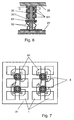
- Fig. 6 shows a section through a further preferred embodiment of the power semiconductor module according to the invention.
- a center disk 311 of the ceramic support element 31 defined in this embodiment a fixed distance of a control contact element in the form of a Gate contact bridge 61 to the electrically conductive base plate 21. Electrical contacting of each semiconductor chip provided control connection (“gate”) takes place via so-called Gate springs 62.
- Fig. 7 shows a plan view of a section along the line C-D of Fig. 6.
Landscapes
- Cooling Or The Like Of Semiconductors Or Solid State Devices (AREA)
Priority Applications (1)
| Application Number | Priority Date | Filing Date | Title |
|---|---|---|---|
| EP03405315A EP1475832A1 (fr) | 2003-05-05 | 2003-05-05 | Module semi-conducteur de puissance à contact par pression |
Applications Claiming Priority (1)
| Application Number | Priority Date | Filing Date | Title |
|---|---|---|---|
| EP03405315A EP1475832A1 (fr) | 2003-05-05 | 2003-05-05 | Module semi-conducteur de puissance à contact par pression |
Publications (1)
| Publication Number | Publication Date |
|---|---|
| EP1475832A1 true EP1475832A1 (fr) | 2004-11-10 |
Family
ID=32982021
Family Applications (1)
| Application Number | Title | Priority Date | Filing Date |
|---|---|---|---|
| EP03405315A Withdrawn EP1475832A1 (fr) | 2003-05-05 | 2003-05-05 | Module semi-conducteur de puissance à contact par pression |
Country Status (1)
| Country | Link |
|---|---|
| EP (1) | EP1475832A1 (fr) |
Cited By (10)
| Publication number | Priority date | Publication date | Assignee | Title |
|---|---|---|---|---|
| US20130043578A1 (en) * | 2011-08-17 | 2013-02-21 | Abb Technology Ag | Presspin, power semiconducter module and semiconducter module assembly with multiple power semiconducter modules |
| WO2013057172A1 (fr) * | 2011-10-21 | 2013-04-25 | Abb Technology Ag | Module semiconducteur de puissance et ensemble module semiconducteur de puissance comprenant de multiples modules semiconducteurs de puissance |
| WO2018051389A1 (fr) * | 2016-09-13 | 2018-03-22 | 三菱電機株式会社 | Module semi-conducteur |
| WO2019043753A1 (fr) * | 2017-08-28 | 2019-03-07 | 三菱電機株式会社 | Électrode ressort |
| WO2019043870A1 (fr) * | 2017-08-31 | 2019-03-07 | 三菱電機株式会社 | Électrode à ressort pour module semi-conducteur de puissance de bloc-presse |
| CN111146169A (zh) * | 2018-11-06 | 2020-05-12 | 株洲中车时代电气股份有限公司 | 一种压接模块用导电碟簧组件 |
| WO2020114660A1 (fr) | 2018-12-07 | 2020-06-11 | Abb Schweiz Ag | Préforme de mode de défaillance de court-circuit hybride pour dispositifs à semi-conducteur de puissance |
| WO2023001356A1 (fr) * | 2021-07-19 | 2023-01-26 | Dynex Semiconductor Limited | Dispositif à semi-conducteurs de puissance avec mécanisme de dérivation de courant |
| EP4148789A1 (fr) * | 2021-09-13 | 2023-03-15 | Infineon Technologies AG | Modules d'alimentation à semi-conducteur |
| WO2026047041A1 (fr) * | 2024-08-29 | 2026-03-05 | Hitachi Energy Ltd | Module semi-conducteur de puissance et procédé de création d'une dérivation de courant dans le module semi-conducteur de puissance |
Citations (6)
| Publication number | Priority date | Publication date | Assignee | Title |
|---|---|---|---|---|
| DE3531471A1 (de) * | 1984-09-03 | 1986-03-20 | Mitsubishi Denki K.K., Tokio/Tokyo | Halbleiter-bauelement vom druckkontakttyp |
| DE3508456A1 (de) * | 1985-03-09 | 1986-09-11 | Brown, Boveri & Cie Ag, 6800 Mannheim | Leistungshalbleitermodul |
| JPH0251275A (ja) * | 1988-08-12 | 1990-02-21 | Fuji Electric Co Ltd | 制御半導体装置 |
| US4956696A (en) * | 1989-08-24 | 1990-09-11 | Sundstrand Corporation | Compression loaded semiconductor device |
| DE4310446C1 (de) * | 1993-03-31 | 1994-05-05 | Export Contor Ausenhandelsgese | Schaltungsanordnung |
| DE19903245A1 (de) * | 1999-01-27 | 2000-08-03 | Asea Brown Boveri | Leistungshalbleitermodul |
-
2003
- 2003-05-05 EP EP03405315A patent/EP1475832A1/fr not_active Withdrawn
Patent Citations (6)
| Publication number | Priority date | Publication date | Assignee | Title |
|---|---|---|---|---|
| DE3531471A1 (de) * | 1984-09-03 | 1986-03-20 | Mitsubishi Denki K.K., Tokio/Tokyo | Halbleiter-bauelement vom druckkontakttyp |
| DE3508456A1 (de) * | 1985-03-09 | 1986-09-11 | Brown, Boveri & Cie Ag, 6800 Mannheim | Leistungshalbleitermodul |
| JPH0251275A (ja) * | 1988-08-12 | 1990-02-21 | Fuji Electric Co Ltd | 制御半導体装置 |
| US4956696A (en) * | 1989-08-24 | 1990-09-11 | Sundstrand Corporation | Compression loaded semiconductor device |
| DE4310446C1 (de) * | 1993-03-31 | 1994-05-05 | Export Contor Ausenhandelsgese | Schaltungsanordnung |
| DE19903245A1 (de) * | 1999-01-27 | 2000-08-03 | Asea Brown Boveri | Leistungshalbleitermodul |
Non-Patent Citations (1)
| Title |
|---|
| PATENT ABSTRACTS OF JAPAN vol. 014, no. 216 (E - 0924) 8 May 1990 (1990-05-08) * |
Cited By (28)
| Publication number | Priority date | Publication date | Assignee | Title |
|---|---|---|---|---|
| US20130043578A1 (en) * | 2011-08-17 | 2013-02-21 | Abb Technology Ag | Presspin, power semiconducter module and semiconducter module assembly with multiple power semiconducter modules |
| KR20130020629A (ko) * | 2011-08-17 | 2013-02-27 | 에이비비 테크놀로지 아게 | 프레스핀, 전력 반도체 모듈 및 다중 전력 반도체 모듈들을 갖는 반도체 모듈 조립체 |
| CN102956570A (zh) * | 2011-08-17 | 2013-03-06 | Abb技术有限公司 | 母座、功率半导体模块以及具有多个功率半导体模块的半导体模块组装件 |
| JP2013048239A (ja) * | 2011-08-17 | 2013-03-07 | Abb Technology Ag | プレスピン、電力半導体モジュール、複数の電力半導体モジュールを備えた半導体モジュール・アセンブリ |
| CN102956570B (zh) * | 2011-08-17 | 2017-06-23 | Abb 技术有限公司 | 母座、功率半导体模块以及具有多个功率半导体模块的半导体模块组装件 |
| WO2013057172A1 (fr) * | 2011-10-21 | 2013-04-25 | Abb Technology Ag | Module semiconducteur de puissance et ensemble module semiconducteur de puissance comprenant de multiples modules semiconducteurs de puissance |
| CN103890941A (zh) * | 2011-10-21 | 2014-06-25 | Abb技术有限公司 | 功率半导体模块和具有多个功率半导体模块的功率半导体模块组件 |
| JP2014531133A (ja) * | 2011-10-21 | 2014-11-20 | アーベーベーテクノロジーアクチエンゲゼルシャフトABB Technology AG | パワー半導体モジュール及び複数のパワー半導体モジュールを備えたパワー半導体モジュールアセンブリ |
| US9035447B2 (en) | 2011-10-21 | 2015-05-19 | Abb Technology Ag | Power semiconductor module and power semiconductor module assembly with multiple power semiconductor modules |
| CN103890941B (zh) * | 2011-10-21 | 2016-10-26 | Abb技术有限公司 | 功率半导体模块和具有多个功率半导体模块的功率半导体模块组件 |
| CN109690768A (zh) * | 2016-09-13 | 2019-04-26 | 三菱电机株式会社 | 半导体模块 |
| CN109690768B (zh) * | 2016-09-13 | 2022-08-16 | 三菱电机株式会社 | 半导体模块 |
| WO2018051389A1 (fr) * | 2016-09-13 | 2018-03-22 | 三菱電機株式会社 | Module semi-conducteur |
| US10593633B2 (en) | 2016-09-13 | 2020-03-17 | Mitsubishi Electric Corporation | Semiconductor module |
| JPWO2018051389A1 (ja) * | 2016-09-13 | 2018-11-15 | 三菱電機株式会社 | 半導体モジュール |
| WO2019043753A1 (fr) * | 2017-08-28 | 2019-03-07 | 三菱電機株式会社 | Électrode ressort |
| JPWO2019043753A1 (ja) * | 2017-08-28 | 2019-12-12 | 三菱電機株式会社 | ばね電極 |
| WO2019043870A1 (fr) * | 2017-08-31 | 2019-03-07 | 三菱電機株式会社 | Électrode à ressort pour module semi-conducteur de puissance de bloc-presse |
| JPWO2019043870A1 (ja) * | 2017-08-31 | 2020-02-06 | 三菱電機株式会社 | プレスパックパワー半導体モジュール用ばね電極 |
| CN111146169A (zh) * | 2018-11-06 | 2020-05-12 | 株洲中车时代电气股份有限公司 | 一种压接模块用导电碟簧组件 |
| WO2020114660A1 (fr) | 2018-12-07 | 2020-06-11 | Abb Schweiz Ag | Préforme de mode de défaillance de court-circuit hybride pour dispositifs à semi-conducteur de puissance |
| CN113169154A (zh) * | 2018-12-07 | 2021-07-23 | Abb电网瑞士股份公司 | 用于功率半导体器件的混合短路故障模式预型件 |
| US11742312B2 (en) | 2018-12-07 | 2023-08-29 | Hitachi Energy Switzerland Ag | Hybrid short circuit failure mode preform for power semiconductor devices |
| CN113169154B (zh) * | 2018-12-07 | 2024-03-22 | 日立能源有限公司 | 用于功率半导体器件的混合短路故障模式预型件 |
| WO2023001356A1 (fr) * | 2021-07-19 | 2023-01-26 | Dynex Semiconductor Limited | Dispositif à semi-conducteurs de puissance avec mécanisme de dérivation de courant |
| EP4148789A1 (fr) * | 2021-09-13 | 2023-03-15 | Infineon Technologies AG | Modules d'alimentation à semi-conducteur |
| US12456654B2 (en) | 2021-09-13 | 2025-10-28 | Infineon Technologies Ag | Power semiconductor modules |
| WO2026047041A1 (fr) * | 2024-08-29 | 2026-03-05 | Hitachi Energy Ltd | Module semi-conducteur de puissance et procédé de création d'une dérivation de courant dans le module semi-conducteur de puissance |
Similar Documents
| Publication | Publication Date | Title |
|---|---|---|
| EP0762496B1 (fr) | Module semi-conducteur de puissance | |
| EP1024530B1 (fr) | Module semiconducteur de puissance | |
| DE19823140B4 (de) | Abtast-Feldeffekttransistor | |
| DE69711083T2 (de) | Kontaktstift für prüfzwecke | |
| DE102009055882A1 (de) | Leistungshalbleitervorrichtung | |
| DE102004028185A1 (de) | Prüfkarte | |
| EP1475832A1 (fr) | Module semi-conducteur de puissance à contact par pression | |
| EP1425799B1 (fr) | Module semi-conducteur de puissance mis en contact par pression | |
| EP1318545A1 (fr) | Sous-module semi-conducteur à haut prestation et module semi-conducteur à haut prestation | |
| DE102011050638B4 (de) | Steckverbindung | |
| DE102017117667B4 (de) | Leistungshalbleitermodul mit einer auf eine Schalteinrichtung einwirkenden Druckeinrichtung | |
| EP0058235A2 (fr) | Appareil de commutation électromagnétique | |
| EP0729179A1 (fr) | Boîtier de contact par pression pour composant semi-conducteur | |
| DE10297047B4 (de) | Lötfreie Leiterplatten-Baugruppe | |
| DE112019007343B4 (de) | Halbleitereinheit | |
| EP1207553A1 (fr) | Dispositif de fixation pour une dispositif semi-conducteur à haut prestation avec des contacts par pression | |
| WO2014166928A1 (fr) | Module de semi-conducteurs de puissance | |
| DE19615112A1 (de) | Leistungshalbleiterbauelement | |
| DE102019128386A1 (de) | Zellkontaktierungsvorrichtung zum Verbinden eines ersten Batterieelements mit einem zweiten Batterieelement eines elektrischen Energiespeichers, sowie elektrischer Energiespeicher | |
| DE102021128835B4 (de) | Schaltungsanordnung mit flächig aufgebrachtem Kondensator | |
| DE102005062444B4 (de) | Halbleitervorrichtungen und Herstellungsverfahren für eine Halbleitervorrichtung | |
| DE60006838T2 (de) | Elektrische anschlussvorrichtung für leistungsschalter | |
| DE102024204484A1 (de) | Elektronikanordnung | |
| EP0053812A2 (fr) | Colonne de thyristors | |
| EP3961818A1 (fr) | Agencement de distribution des potentiels |
Legal Events
| Date | Code | Title | Description |
|---|---|---|---|
| PUAI | Public reference made under article 153(3) epc to a published international application that has entered the european phase |
Free format text: ORIGINAL CODE: 0009012 |
|
| AK | Designated contracting states |
Kind code of ref document: A1 Designated state(s): AT BE BG CH CY CZ DE DK EE ES FI FR GB GR HU IE IT LI LU MC NL PT RO SE SI SK TR |
|
| AX | Request for extension of the european patent |
Extension state: AL LT LV MK |
|
| AKX | Designation fees paid | ||
| REG | Reference to a national code |
Ref country code: DE Ref legal event code: 8566 |
|
| STAA | Information on the status of an ep patent application or granted ep patent |
Free format text: STATUS: THE APPLICATION IS DEEMED TO BE WITHDRAWN |
|
| 18D | Application deemed to be withdrawn |
Effective date: 20050511 |