EP1475840A1 - Verfahren zur Herstellung einer elektrischen Speichereinrichtung mit Auswahltransistoren für Speicherelemente sowie entsprechend hergestellte Speichereinrichtung - Google Patents
Verfahren zur Herstellung einer elektrischen Speichereinrichtung mit Auswahltransistoren für Speicherelemente sowie entsprechend hergestellte Speichereinrichtung Download PDFInfo
- Publication number
- EP1475840A1 EP1475840A1 EP03425292A EP03425292A EP1475840A1 EP 1475840 A1 EP1475840 A1 EP 1475840A1 EP 03425292 A EP03425292 A EP 03425292A EP 03425292 A EP03425292 A EP 03425292A EP 1475840 A1 EP1475840 A1 EP 1475840A1
- Authority
- EP
- European Patent Office
- Prior art keywords
- raised
- conductive region
- forming
- memory device
- layer
- Prior art date
- Legal status (The legal status is an assumption and is not a legal conclusion. Google has not performed a legal analysis and makes no representation as to the accuracy of the status listed.)
- Granted
Links
- 238000003860 storage Methods 0.000 title claims abstract description 37
- 238000000034 method Methods 0.000 title claims abstract description 35
- 238000004519 manufacturing process Methods 0.000 title claims abstract description 15
- 239000004065 semiconductor Substances 0.000 claims abstract description 8
- 229910021332 silicide Inorganic materials 0.000 claims description 11
- FVBUAEGBCNSCDD-UHFFFAOYSA-N silicide(4-) Chemical compound [Si-4] FVBUAEGBCNSCDD-UHFFFAOYSA-N 0.000 claims description 11
- 238000005530 etching Methods 0.000 claims description 8
- 238000000926 separation method Methods 0.000 claims 7
- 230000001681 protective effect Effects 0.000 claims 2
- 239000000463 material Substances 0.000 description 17
- 229910021420 polycrystalline silicon Inorganic materials 0.000 description 15
- 229920005591 polysilicon Polymers 0.000 description 15
- 230000015654 memory Effects 0.000 description 11
- 238000005468 ion implantation Methods 0.000 description 7
- VYPSYNLAJGMNEJ-UHFFFAOYSA-N Silicium dioxide Chemical compound O=[Si]=O VYPSYNLAJGMNEJ-UHFFFAOYSA-N 0.000 description 6
- 125000006850 spacer group Chemical group 0.000 description 6
- 238000000151 deposition Methods 0.000 description 5
- 238000010438 heat treatment Methods 0.000 description 5
- 239000000758 substrate Substances 0.000 description 5
- XUIMIQQOPSSXEZ-UHFFFAOYSA-N Silicon Chemical compound [Si] XUIMIQQOPSSXEZ-UHFFFAOYSA-N 0.000 description 4
- 239000003989 dielectric material Substances 0.000 description 4
- 150000002500 ions Chemical class 0.000 description 4
- 238000002955 isolation Methods 0.000 description 4
- 150000004767 nitrides Chemical class 0.000 description 4
- 229910052710 silicon Inorganic materials 0.000 description 3
- 239000010703 silicon Substances 0.000 description 3
- 235000012239 silicon dioxide Nutrition 0.000 description 3
- 239000000377 silicon dioxide Substances 0.000 description 3
- 229910045601 alloy Inorganic materials 0.000 description 2
- 239000000956 alloy Substances 0.000 description 2
- 239000011248 coating agent Substances 0.000 description 2
- 238000000576 coating method Methods 0.000 description 2
- 239000004020 conductor Substances 0.000 description 2
- 238000002425 crystallisation Methods 0.000 description 2
- 230000008025 crystallization Effects 0.000 description 2
- 238000011049 filling Methods 0.000 description 2
- 230000008018 melting Effects 0.000 description 2
- 238000002844 melting Methods 0.000 description 2
- 230000000737 periodic effect Effects 0.000 description 2
- 230000003213 activating effect Effects 0.000 description 1
- 150000004770 chalcogenides Chemical class 0.000 description 1
- 230000008021 deposition Effects 0.000 description 1
- 239000002019 doping agent Substances 0.000 description 1
- 230000000694 effects Effects 0.000 description 1
- 230000001771 impaired effect Effects 0.000 description 1
- 230000010354 integration Effects 0.000 description 1
- 239000002184 metal Substances 0.000 description 1
- 238000012986 modification Methods 0.000 description 1
- 230000004048 modification Effects 0.000 description 1
- 230000006911 nucleation Effects 0.000 description 1
- 238000010899 nucleation Methods 0.000 description 1
- -1 on raised regions 35 Chemical compound 0.000 description 1
- 238000005498 polishing Methods 0.000 description 1
- 239000010409 thin film Substances 0.000 description 1
Images




Classifications
-
- H—ELECTRICITY
- H10—SEMICONDUCTOR DEVICES; ELECTRIC SOLID-STATE DEVICES NOT OTHERWISE PROVIDED FOR
- H10B—ELECTRONIC MEMORY DEVICES
- H10B63/00—Resistance change memory devices, e.g. resistive RAM [ReRAM] devices
- H10B63/30—Resistance change memory devices, e.g. resistive RAM [ReRAM] devices comprising selection components having three or more electrodes, e.g. transistors
- H10B63/32—Resistance change memory devices, e.g. resistive RAM [ReRAM] devices comprising selection components having three or more electrodes, e.g. transistors of the bipolar type
-
- H—ELECTRICITY
- H10—SEMICONDUCTOR DEVICES; ELECTRIC SOLID-STATE DEVICES NOT OTHERWISE PROVIDED FOR
- H10N—ELECTRIC SOLID-STATE DEVICES NOT OTHERWISE PROVIDED FOR
- H10N70/00—Solid-state devices having no potential barriers, and specially adapted for rectifying, amplifying, oscillating or switching
- H10N70/20—Multistable switching devices, e.g. memristors
- H10N70/231—Multistable switching devices, e.g. memristors based on solid-state phase change, e.g. between amorphous and crystalline phases, Ovshinsky effect
-
- H—ELECTRICITY
- H10—SEMICONDUCTOR DEVICES; ELECTRIC SOLID-STATE DEVICES NOT OTHERWISE PROVIDED FOR
- H10N—ELECTRIC SOLID-STATE DEVICES NOT OTHERWISE PROVIDED FOR
- H10N70/00—Solid-state devices having no potential barriers, and specially adapted for rectifying, amplifying, oscillating or switching
- H10N70/801—Constructional details of multistable switching devices
- H10N70/821—Device geometry
- H10N70/826—Device geometry adapted for essentially vertical current flow, e.g. sandwich or pillar type devices
-
- H—ELECTRICITY
- H10—SEMICONDUCTOR DEVICES; ELECTRIC SOLID-STATE DEVICES NOT OTHERWISE PROVIDED FOR
- H10N—ELECTRIC SOLID-STATE DEVICES NOT OTHERWISE PROVIDED FOR
- H10N70/00—Solid-state devices having no potential barriers, and specially adapted for rectifying, amplifying, oscillating or switching
- H10N70/801—Constructional details of multistable switching devices
- H10N70/841—Electrodes
- H10N70/8413—Electrodes adapted for resistive heating
Definitions
- the present invention relates to a process for manufacturing a memory device having selector transistors for storage elements and to a memory device fabricated thereby.
- memory devices comprise a plurality of memory cells or storage elements arranged in rows and columns, so as to form a memory array.
- Row and column decoders are used to selectively connect the storage elements to read/write circuits of the memory device for usual operation through.
- further selection elements which selectively activate and deactivate the storage elements for preventing disturbances caused by other adjacent storage elements.
- bipolar transistors as selectors coupled to the storage elements.
- a bipolar selector transistor has a base terminal connected to a control line (e.g. a word line), an emitter terminal coupled to the storage element and a collector terminal normally connected to ground. It is clear that the way the emitter of the bipolar selector transistor and the storage element are coupled depends on the structure of the storage element itself.
- phase change memories are presently memory devices of increasing interest, which use bipolar transistors as selectors for storage elements.
- Phase change memory cells utilize a class of materials that have the unique property of being reversibly switcheable from one phase to another with measurable distinct electrical properties associated with each phase. For example, these materials may change between an amorphous disordered phase and a crystalline, or polycrystalline, ordered phase.
- a material property that may change and provide a signature for each phase is the material resistivity, which is considerably different in the two states.
- phase change cells are alloys of elements of the VI group of the periodic table as Te or Se, also called chalcogenides or chalcogenic materials. Therefore, hereinafter, the term "chalcogenic materials" is used to indicate all materials switcheable between at least two different phases where they have different electrical properties (resistances) and include thus the elements of the VI group of the periodic table and their alloys.
- phase change memories In phase change memories, a thin film of chalcogenic material is employed as a programmable resistor, switching between a high and a low resistance condition.
- Phase change is normally obtained by locally increasing the temperature. Under 150°C, both phases are stable. Over 200°C, nucleation of crystallites is fast and if the material is kept at the crystallization temperature for a sufficient time, it changes phase and becomes crystalline. In order to change the phase back to the amorphous state, its temperature is brought over the melting point (about 600°C) and the calcogenide is rapidly cooled.
- the state of the chalcogenic material may be read applying a sufficiently small voltage (or current) so as not to cause a sensible heating and measuring the current passing through it (or voltage across it). Since the current is proportional to the conductance of the chalcogenic material (or voltage is proportional to the resistance), it is possible to discriminate between the two states.
- bipolar selector transistors are coupled to the chalcogenic storage elements.
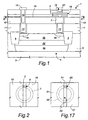
- figure 1 illustrates a portion of a phase change memory device 1, comprising a chalcogenic strip 2, a cup-shaped heater 3, filled with dielectric material, and a selector 4;
- the selector 4 is a PNP bipolar transistor and is built in an epitaxial layer 5 grown over a substrate 7.
- the selector 4 comprises an emitter region 4a, a base region 4b, having a base contact region 4c, a collector region 4d and a sub-collector region 4e; moreover, the selector 4 is laterally delimited by trench isolation structures 9.
- a storage element 8 is defined at a contact region between the chalcogenic strip 2 and the heater 3, as schematically shown in figure 2.
- the heater 3 must be located a distance apart from the selector 4 and therefore is embedded in an upper dielectric layer 10, which is deposited on a lower dielectric layer 11.
- the heater 3 is connected to the emitter region 4a of the selector 4 through a first plug 12, extending across the lower dielectric layer 11.
- a second plug 13 connects the base contact region 4c of the selector 4 to a word line 15.
- the selector 4 is initially formed inside the epitaxial layer 5. Then, the lower dielectric layer 11 is deposited on the epitaxial layer 5 and the plugs 12, 13 are fabricated. More precisely, the lower dielectric layer 11 is anisotropically etched so as to form through openings, which are internally coated with a first conductive material and subsequently filled with a second conductive material.
- the upper dielectric layer 10 is then deposited on the lower dielectric layer 11 and the heater 3 is made therein, by etching the upper dielectric layer 10, so as to open a cavity over the first plug 12, by coating the cavity with a material having a predetermined resistivity, thus contacting the first plug 12, and by filling the cavity again with dielectric material.
- a delimiting layer 16 having an aperture is built on the upper dielectric layer 10; a chalcogenic layer is deposited on the delimiting layer 16 and fills the aperture, thereby forming the chalcogenic strip 2 and the storage element 8.
- connection lines 20 are made, according to a required layout.
- fabricating the heater 3 preliminarily requires depositing the lower dielectric layer 11, for thermally insulating the selector 4 from the heater 3, forming the first plug 12 and the second plug 13 (i.e. etching the lower dielectric layer 11, internally coating and filling the openings), depositing and etching the upper dielectric layer 10; only at this stage of the process, resistive material can be deposited to form the heater 3.
- plugs 12, 13 land directly on doped epitaxial silicon of emitter region 4a and base contact region 4c, whereas further processing for making the surface of silicon contact regions highly conductive would be desirable.
- the object of the invention is thus to provide a process for manufacturing memory devices and a memory device that overcome the above described drawbacks.
- a process for manufacturing a memory device having selector transistors for storage elements and a memory device fabricated thereby are provided, as defined respectively in claims 1 and 24.
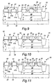
- a wafer 20 of semiconductor material comprises a substrate 21 and an epitaxial layer 22, for example of P type and of P- type, respectively.
- a bipolar selector transistor 25 is formed within the epitaxial layer 21, in a per se known manner.
- the selector 25 is laterally delimited by trench isolation structures 24, preferably of silicon dioxide, and comprises a base region 26, of N type, a collector region 27, of P type, contiguous to the base region 26, and a sub-collector region 28, of P+ type and extending between the collector region 27 and the substrate 21.
- a low-voltage gate oxide layer hereinafter designed as LV oxide 30, is thermally grown on a whole surface 20a of the wafer 20 and is defined by a masked etch, so as to open emitter windows 31 and a base window 32, which partially expose corresponding contact areas of the base region 26. More precisely, the emitter windows 31 are formed at sides of the base region 26 and are adjacent to the trench isolation structures 24, whereas the base window 32 exposes a central portion of the base region 26.
- a polysilicon layer 33 of preferably 100-300 nm is deposited on the wafer 20 and entirely covers the LV oxide 30, as shown in figure 4.
- the polysilicon layer 33 and the base region 26 are separated from each other by the LV oxide 30; however, the polysilicon layer 33 extends through the emitter windows 31 and the base window 32, thus reaching the base region 26 at the exposed contact areas.
- the polysilicon layer 33 and the LV oxide 30 are selectively etched using a mask, here not illustrated.
- raised emitter regions 35 and a raised base region 36 are formed on the base region 26 of the selector 25, by removing the polysilicon layer 33 and the LV oxide 30 between the windows 31, 32.
- the raised emitter regions 35 and a raised base region 36 slightly exceed the width of the base region 26.
- LV oxide 30 is at first used as a stop layer when the polysilicon layer 33 is etched, thus preventing the base region 26 from being damaged; then, the LV oxide 30 is etched as well.
- Raised emitter regions 35 and raised base region 36 are spaced by a predetermined distance, as explained hereinafter, and preferably overlap residual portions 30' of the LV oxide 30; such residual portions 30' are not removed to avoid the risk of leaving the base region 26 unprotected during polysilicon etch, on account of possible misalignments of the masks.
- gate oxide regions 38 and gate regions 39 of NMOS transistors 40 and PMOS transistors 41 are formed.
- a protecting layer 43 e.g. of silicon dioxide, illustrated with a dotted line in figure 7, is then formed on the entire wafer 20 and is anisotropically etched.
- the protecting layer 43 is completely removed from substantially flat or smoothed portions of the wafer 20, whereas steep regions remain covered by spacers 45.
- the height of the protecting layer 43 is much greater than elsewhere. Accordingly, the protecting layer 43 is only partially removed, when anisotropically etched, since only portions having lower thickness are completely ablated: so, the spacers 45 are formed and protect the underlying regions.
- the raised emitter regions 35 and the raised base region 36 are reciprocally spaced by such a distance that adjacent spacers 45 join together. Hence, the entire base region 26 is covered by either the raised regions 35, 36, or the spacers 45.
- a P+ ion implantation and a N+ ion implantation are carried out (figures 8 and 9). More precisely, during the P+ ion implantation, the raised emitter regions 35 and the gate regions 39 of PMOS transistors 41 are exposed to receive implanted ions, and the raised base region 36 and the gate regions 39 of NMOS transistors 40 are protected by a first mask 46; on the contrary, during N+ ion implantation the raised base region 36 and the gate regions 39 of NMOS transistors 40 are exposed and the raised emitter regions 35 and the gate regions 39 of PMOS transistors 41 are protected by a second mask 47.
- source regions 40a, 41a and drain regions 40b, 41b of the NMOS transistor 40 and of the PMOS transistor 41 are formed in the epitaxial layer 22 (source regions 40a, 40b and drain regions 41a, 41b are only schematically sketched).
- the wafer 20 is heated for diffusing and activating the implanted ions, as illustrated in figure 10.
- embedded emitter regions 49, of P+ type, and a base contact region 50, of N+ type are formed within the base region 26 under the raised emitter regions 35 and under the raised base region 36, respectively.
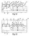
- a self-aligned silicidation step is carried out (figures 11 and 12).
- a metallic layer 51 e.g. of Ti
- metallic silicide regions 52 are formed (figure 12), having higher conductivity than even heavily doped polysilicon, by a coefficient comprised between about 10 and 100; by a selective etch, the metallic layer 51 is removed, whereas the silicide regions 52 are left.
- the metallic layer 51 is locally changed to metallic silicide, by exploiting silicon atoms of the underlying raised emitter regions 35 and of the raised base region 36.
- the silicide regions 52 thus form high conductivity superficial layers of the raised emitter regions 35 and of the raised base region 36. Since the self-aligned silicidation step exploits the conformation of the top surface of the wafer 20 and conductive regions which must be preserved from silicidation are protected by the spacers 45, no anti-silicidation mask is required.
- a nitride layer 54 and a thick dielectric layer 55 are deposited on the wafer 20, which is then planarized, for example by CMP (Chemical-Mechanical-Polishing).
- CMP Chemical-Mechanical-Polishing
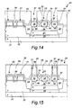
- the nitride layer 54 and the thick dielectric layer 55 are etched and first cavities 57 are opened, which extend down to the raised emitter regions 35, as shown in figure 14; more precisely, the first cavities 57 extend to the silicide regions 52 covering the raised emitter regions 35.
- a heating layer 58 having a predetermined resistivity, is deposited on the entire wafer 20 and coats the thick dielectric layer 55, walls of the first cavities 57 and the silicide regions 52 covering the raised emitter regions 35. Then, the first cavities 57 are filled with dielectric material 59. The dielectric material 59 and the heating layer 58 are removed by CMP from the thick dielectric layer 55 outside the first cavities 57. Residual portions of the heating layer 58 inside the first cavities 57 form heaters 60. Hence, heaters 60 are directly in contact with silicide regions 52 of respective raised emitter regions 35.
- a first level plug 61 is formed for providing electrical connection to the raised base region 36.
- a second cavity 62 is opened through the thick dielectric layer 55 and the nitride layer 54, so as to expose the silicide region 52 covering the raised base region 36; and a first conductive layer 63 is deposited inside the second cavity 62, which is filled with a second conductive layer 64.
- storage elements 65 are made over the heaters 60 (se also figure 17), for example by forming a delimiting layer 67 having apertures 68 and by depositing and defining a chalcogenic layer 70, which fills the apertures 68. Accordingly, a memory device 75 is obtained, in which storage elements 65 are stacked on the selector 25 and the heaters 63; moreover, the storage elements 65 are connected to respective raised emitter regions 35 of the selector 25 through respective heaters 63.
- an insulating layer 71 is deposited on the wafer 20; storage contacts 72 and a second level plug 73 are formed through insulating layer 71, so as to reach the storage elements 65 and the first level plug 61, respectively.
- the process is quite simple with respect to the known processes.
- silicidation step is self-aligned, since it is carried out exploiting the superficial conformation of the wafer and anti-silicidation mask is advantageously eliminated.
- the heaters are made inside the dielectric layer which delimits the raised regions and therefore their fabrication does not require further deposition of dielectric layers.
- the present memory and manufacturing process allow a very efficient integration, completely compatible with CMOS technology and also with processes for the fabrication of chalcogenic storage elements with sublithographic dimension.
- selectors having raised emitter and/or base regions are provided, with high quality emitter and base contacts.
- raised regions can be easily silicidised and the components that are coupled to the emitter and base contacts (i.e. heaters and first level plugs, respectively) land directly on silicide interfaces, which are much more conductive than polysilicon.
- intermediate contacts are avoided.
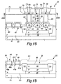
- the selector 25 is formed inside a wafer 20', which comprises the substrate 21, the epitaxial layer 22 and the trench isolation structures 24, as formerly described; moreover source regions 40a, 41a and drain regions 40b, 41b of transistors 40, 41 are formed in the substrate 22.
- a LV oxide layer 80 and a polysilicon layer 81 are grown on the wafer 20' and selectively etched for defining the gate oxide regions 38 and gate regions 39 of transistors 40, 41.
- the polysilicon layer 81 is removed from the base region 26.
- a nitride layer 82 and a dielectric layer 83 are then deposited, planarized by CMP and etched, so as to open emitter apertures 85 and a base aperture 86 over the base region 26, and gate apertures 87 over the gate regions 39 of the transistors 40, 41 (figure 19).
- the LV oxide layer 80 is then removed inside the emitter apertures 85 and the base aperture 86; hence, the base region 26 is partially exposed.
- a hard mask 89 is then formed, which protects the entire wafer 20', except the emitter apertures 83 and the base aperture 84.
- an epitaxial growth step is carried out, during which epitaxial regions are formed over exposed portions of the base region 26.
- the epitaxial regions comprise raised emitter regions 91, inside the emitter apertures 85, and a raised base region 92, inside the base aperture 86.
- the process can be exploited for manufacturing any kind of memories that require bipolar selector transistors coupled to the storage elements, and not only phase change memories.
- the selector 25 can comprise either a single raised emitter or even more than two raised emitters. Moreover, the selector 25 could have only raised emitter regions, whereas the base contact is of a standard type. In this case, the LV oxide 30 is removed only to open emitter windows 31 and is left elsewhere over the base region 26. After building the spacers 45, a portion of the base region 26 is exposed, so that it first receives N+ type dopant ions, and then is coated by a silicide region during silicidation. Also in this case, silicidation is self-aligned and anti-silicidation mask is not required. A deeper first level plug is formed later, since it has to go through all the thickness of the thick dielectric layer 55; anyway the quality of the base contact is not impaired.
- the LV oxide 30 can be completely etched over the base region 26, before depositing the polysilicon layer 33 directly on the base region 26 itself.
- the polysilicon layer 33 is then etched as described, for defining the raised emitter regions 35 over the base region 26 and the gate regions 39 in circuitry area; the etch of the polysilicon layer 33 is stopped as soon as the residual LV oxide 30 in the circuitry area is reached and a slight over-etch of the base region 26 is accepted.
- the first and second level plugs 61 and 73 can be replaced by a single level plug, thus simplifying the process.
- the selector 25 can be also a bipolar NPN transistor.
Landscapes
- Semiconductor Memories (AREA)
- Bipolar Transistors (AREA)
Priority Applications (3)
| Application Number | Priority Date | Filing Date | Title |
|---|---|---|---|
| EP03425292A EP1475840B1 (de) | 2003-05-07 | 2003-05-07 | Verfahren zur Herstellung einer elektrischen Speichereinrichtung mit Auswahltransistoren für Speicherelemente sowie entsprechend hergestellte Speichereinrichtung |
| DE60306893T DE60306893T2 (de) | 2003-05-07 | 2003-05-07 | Verfahren zur Herstellung einer elektrischen Speichereinrichtung mit Auswahltransistoren für Speicherelemente sowie entsprechend hergestellte Speichereinrichtung |
| US10/836,651 US20050024933A1 (en) | 2003-05-07 | 2004-04-30 | Process for manufacturing device having selector transistors for storage elements and memory device fabricated thereby |
Applications Claiming Priority (1)
| Application Number | Priority Date | Filing Date | Title |
|---|---|---|---|
| EP03425292A EP1475840B1 (de) | 2003-05-07 | 2003-05-07 | Verfahren zur Herstellung einer elektrischen Speichereinrichtung mit Auswahltransistoren für Speicherelemente sowie entsprechend hergestellte Speichereinrichtung |
Publications (2)
| Publication Number | Publication Date |
|---|---|
| EP1475840A1 true EP1475840A1 (de) | 2004-11-10 |
| EP1475840B1 EP1475840B1 (de) | 2006-07-19 |
Family
ID=32982046
Family Applications (1)
| Application Number | Title | Priority Date | Filing Date |
|---|---|---|---|
| EP03425292A Expired - Lifetime EP1475840B1 (de) | 2003-05-07 | 2003-05-07 | Verfahren zur Herstellung einer elektrischen Speichereinrichtung mit Auswahltransistoren für Speicherelemente sowie entsprechend hergestellte Speichereinrichtung |
Country Status (3)
| Country | Link |
|---|---|
| US (1) | US20050024933A1 (de) |
| EP (1) | EP1475840B1 (de) |
| DE (1) | DE60306893T2 (de) |
Cited By (9)
| Publication number | Priority date | Publication date | Assignee | Title |
|---|---|---|---|---|
| DE102004059428A1 (de) * | 2004-12-09 | 2006-06-22 | Infineon Technologies Ag | Herstellungsverfahren für eine mikroelektronische Elektrodenstruktur, insbesondere für ein PCM-Speicherelement, und entsprechende mikroelektronische Elektrodenstruktur |
| EP1677372A1 (de) * | 2004-12-30 | 2006-07-05 | STMicroelectronics S.r.l. | Phasenwechselspeicher und Herstellungsmethode dafür |
| EP1845567A1 (de) * | 2006-04-11 | 2007-10-17 | STMicroelectronics S.r.l. | Phasenwechselspeicherelement und Herstellungsprozess dafür |
| WO2007143387A3 (en) * | 2006-05-31 | 2008-01-31 | Sandisk 3D Llc | Conductive hard mask to protect patterned features during trench etch |
| WO2008097910A3 (en) * | 2007-02-05 | 2008-11-27 | Marvell World Trade Ltd | Phase change memory devices with,bipolar transitstors and manufacturing methods thereof |
| EP2015357A1 (de) | 2007-07-09 | 2009-01-14 | STMicroelectronics S.r.l. | Herstellungsverfahren für ein Zellenfeld mit bipolaren Auswahltransistoren mit hervorstehenden leitfähigen Bereichen |
| US7737049B2 (en) | 2007-07-31 | 2010-06-15 | Qimonda Ag | Method for forming a structure on a substrate and device |
| WO2010076825A1 (en) * | 2008-12-30 | 2010-07-08 | Fabio Pellizer | Double patterning method for creating a regular array of pillars with dual shallow trench isolation |
| CN103151458A (zh) * | 2013-03-22 | 2013-06-12 | 厦门博佳琴电子科技有限公司 | 一种嵌入式相变化存储器阵列及制造方法 |
Families Citing this family (11)
| Publication number | Priority date | Publication date | Assignee | Title |
|---|---|---|---|---|
| CN1954428B (zh) * | 2004-05-14 | 2010-09-29 | 株式会社瑞萨科技 | 半导体存储器件 |
| EP1677371A1 (de) * | 2004-12-30 | 2006-07-05 | STMicroelectronics S.r.l. | Zweiteiliger Widerstandsheizer für Phasenwechselspeicher und Herstellungsmethode |
| US7745809B1 (en) * | 2007-04-03 | 2010-06-29 | Marvell International Ltd. | Ultra high density phase change memory having improved emitter contacts, improved GST cell reliability and highly matched UHD GST cells using column mirco-trench strips |
| US7848133B2 (en) * | 2007-12-31 | 2010-12-07 | Intel Corporation | Phase change memory with bipolar junction transistor select device |
| US8599599B2 (en) * | 2011-09-01 | 2013-12-03 | Micron Technology, Inc. | Method, system, and device for phase change memory switch wall cell with approximately horizontal electrode contact |
| TWI587454B (zh) * | 2016-05-09 | 2017-06-11 | 光磊科技股份有限公司 | 具備記憶元件與選擇器功能之單一記憶胞結構 |
| US10510954B2 (en) | 2017-11-28 | 2019-12-17 | Taiwan Semiconductor Manufacturing Co., Ltd. | Phase change random access memory device |
| FR3096827A1 (fr) * | 2019-05-28 | 2020-12-04 | Stmicroelectronics (Crolles 2) Sas | Mémoire à changement de phase |
| US12150393B2 (en) | 2022-09-30 | 2024-11-19 | International Business Machines Corporation | Heater for phase change material memory cell |
| US20240407178A1 (en) * | 2023-06-05 | 2024-12-05 | International Business Machines Corporation | Phase change memory cell with crystalline structure aligned to seed layer |
| FR3162311A1 (fr) * | 2024-05-14 | 2025-11-21 | Stmicroelectronics International N.V. | Procédé de fabrication d'un dispositif électronique comprenant un circuit mémoire |
Citations (5)
| Publication number | Priority date | Publication date | Assignee | Title |
|---|---|---|---|---|
| US4922318A (en) * | 1985-09-18 | 1990-05-01 | Advanced Micro Devices, Inc. | Bipolar and MOS devices fabricated on same integrated circuit substrate |
| EP0544204A1 (de) * | 1991-11-26 | 1993-06-02 | Nec Corporation | Nichtflüchtige Halbleiterspeicheranordnung mit über den entsprechend verknüpften Auswahltransistoren gestapelten Dünnschichtspeichertransistoren |
| WO2000057498A1 (en) * | 1999-03-25 | 2000-09-28 | Energy Conversion Devices, Inc. | Electrically programmable memory element with improved contacts |
| US20020038883A1 (en) * | 2000-09-29 | 2002-04-04 | Lowrey Tyler A. | Compositionally modified resistive electrode |
| EP1318552A1 (de) * | 2001-12-05 | 2003-06-11 | STMicroelectronics S.r.l. | Kleinflächige Kontaktzone, hocheffizientes Phasenwechsel-Speicherelement und dessen Verfahren zur Herstellung |
Family Cites Families (5)
| Publication number | Priority date | Publication date | Assignee | Title |
|---|---|---|---|---|
| US5134454A (en) * | 1990-09-26 | 1992-07-28 | Purdue Research Foundation | Self-aligned integrated circuit bipolar transistor having monocrystalline contacts |
| TW383459B (en) * | 1997-12-19 | 2000-03-01 | United Microelectronics Corp | Manufacturing method for bit line |
| US6531373B2 (en) * | 2000-12-27 | 2003-03-11 | Ovonyx, Inc. | Method of forming a phase-change memory cell using silicon on insulator low electrode in charcogenide elements |
| US6617220B2 (en) * | 2001-03-16 | 2003-09-09 | International Business Machines Corporation | Method for fabricating an epitaxial base bipolar transistor with raised extrinsic base |
| JP2004079138A (ja) * | 2002-08-22 | 2004-03-11 | Renesas Technology Corp | 不揮発性半導体記憶装置 |
-
2003
- 2003-05-07 EP EP03425292A patent/EP1475840B1/de not_active Expired - Lifetime
- 2003-05-07 DE DE60306893T patent/DE60306893T2/de not_active Expired - Lifetime
-
2004
- 2004-04-30 US US10/836,651 patent/US20050024933A1/en not_active Abandoned
Patent Citations (5)
| Publication number | Priority date | Publication date | Assignee | Title |
|---|---|---|---|---|
| US4922318A (en) * | 1985-09-18 | 1990-05-01 | Advanced Micro Devices, Inc. | Bipolar and MOS devices fabricated on same integrated circuit substrate |
| EP0544204A1 (de) * | 1991-11-26 | 1993-06-02 | Nec Corporation | Nichtflüchtige Halbleiterspeicheranordnung mit über den entsprechend verknüpften Auswahltransistoren gestapelten Dünnschichtspeichertransistoren |
| WO2000057498A1 (en) * | 1999-03-25 | 2000-09-28 | Energy Conversion Devices, Inc. | Electrically programmable memory element with improved contacts |
| US20020038883A1 (en) * | 2000-09-29 | 2002-04-04 | Lowrey Tyler A. | Compositionally modified resistive electrode |
| EP1318552A1 (de) * | 2001-12-05 | 2003-06-11 | STMicroelectronics S.r.l. | Kleinflächige Kontaktzone, hocheffizientes Phasenwechsel-Speicherelement und dessen Verfahren zur Herstellung |
Cited By (17)
| Publication number | Priority date | Publication date | Assignee | Title |
|---|---|---|---|---|
| DE102004059428A1 (de) * | 2004-12-09 | 2006-06-22 | Infineon Technologies Ag | Herstellungsverfahren für eine mikroelektronische Elektrodenstruktur, insbesondere für ein PCM-Speicherelement, und entsprechende mikroelektronische Elektrodenstruktur |
| US7317201B2 (en) | 2004-12-09 | 2008-01-08 | Infineon Technologies Ag | Method of producing a microelectronic electrode structure, and microelectronic electrode structure |
| EP1677372A1 (de) * | 2004-12-30 | 2006-07-05 | STMicroelectronics S.r.l. | Phasenwechselspeicher und Herstellungsmethode dafür |
| WO2006069933A1 (en) * | 2004-12-30 | 2006-07-06 | Stmicroelectronics S.R.L. | Phase change memory and manufacturing method thereof |
| CN101142695B (zh) * | 2004-12-30 | 2010-12-08 | 意法半导体股份有限公司 | 相变存储器及其制造方法 |
| US7709822B2 (en) | 2004-12-30 | 2010-05-04 | Stmicroeletronics S.R.L. | Phase change memory and manufacturing method thereof |
| EP1845567A1 (de) * | 2006-04-11 | 2007-10-17 | STMicroelectronics S.r.l. | Phasenwechselspeicherelement und Herstellungsprozess dafür |
| US7575984B2 (en) | 2006-05-31 | 2009-08-18 | Sandisk 3D Llc | Conductive hard mask to protect patterned features during trench etch |
| WO2007143387A3 (en) * | 2006-05-31 | 2008-01-31 | Sandisk 3D Llc | Conductive hard mask to protect patterned features during trench etch |
| US8722518B2 (en) | 2006-05-31 | 2014-05-13 | Sandisk 3D Llc | Methods for protecting patterned features during trench etch |
| WO2008097910A3 (en) * | 2007-02-05 | 2008-11-27 | Marvell World Trade Ltd | Phase change memory devices with,bipolar transitstors and manufacturing methods thereof |
| US7834341B2 (en) | 2007-02-05 | 2010-11-16 | Marvell World Trade Ltd. | Phase change material (PCM) memory devices with bipolar junction transistors and methods for making thereof |
| EP2015357A1 (de) | 2007-07-09 | 2009-01-14 | STMicroelectronics S.r.l. | Herstellungsverfahren für ein Zellenfeld mit bipolaren Auswahltransistoren mit hervorstehenden leitfähigen Bereichen |
| US7737049B2 (en) | 2007-07-31 | 2010-06-15 | Qimonda Ag | Method for forming a structure on a substrate and device |
| WO2010076825A1 (en) * | 2008-12-30 | 2010-07-08 | Fabio Pellizer | Double patterning method for creating a regular array of pillars with dual shallow trench isolation |
| CN103151458A (zh) * | 2013-03-22 | 2013-06-12 | 厦门博佳琴电子科技有限公司 | 一种嵌入式相变化存储器阵列及制造方法 |
| CN103151458B (zh) * | 2013-03-22 | 2015-04-29 | 厦门博佳琴电子科技有限公司 | 一种嵌入式相变化存储器阵列及制造方法 |
Also Published As
| Publication number | Publication date |
|---|---|
| US20050024933A1 (en) | 2005-02-03 |
| DE60306893D1 (de) | 2006-08-31 |
| DE60306893T2 (de) | 2007-02-01 |
| EP1475840B1 (de) | 2006-07-19 |
Similar Documents
| Publication | Publication Date | Title |
|---|---|---|
| EP1475840B1 (de) | Verfahren zur Herstellung einer elektrischen Speichereinrichtung mit Auswahltransistoren für Speicherelemente sowie entsprechend hergestellte Speichereinrichtung | |
| US7227171B2 (en) | Small area contact region, high efficiency phase change memory cell and fabrication method thereof | |
| US6891747B2 (en) | Phase change memory cell and manufacturing method thereof using minitrenches | |
| US7259040B2 (en) | Process for manufacturing a phase change memory array in Cu-damascene technology and phase change memory array manufactured thereby | |
| US7244956B2 (en) | Self-aligned process for manufacturing a phase change memory cell and phase change memory cell thereby manufactured | |
| US12484460B2 (en) | Phase-change memory cell having a compact structure | |
| US7402455B2 (en) | Manufacturing method of a contact structure and phase change memory cell with elimination of double contacts | |
| EP1965427A1 (de) | Matrix vertikaler Bipolartransistoren, insbesondere Auswahlschalter in einer Phasenwechsel-Speichervorrichtung | |
| US7919767B2 (en) | Semiconductor memory device and fabrication method thereof | |
| JP7750968B2 (ja) | 相変化メモリ・セル抵抗性ライナー | |
| US7606056B2 (en) | Process for manufacturing a phase change memory array in Cu-damascene technology and phase change memory array thereby manufactured | |
| US8293598B2 (en) | Process for manufacturing a memory device including a vertical bipolar junction transistor and a CMOS transistor with spacers | |
| US6974734B2 (en) | Process for manufacturing a memory device, in particular a phase change memory, including a silicidation step | |
| US9570681B2 (en) | Resistive random access memory | |
| US12150393B2 (en) | Heater for phase change material memory cell | |
| US5741731A (en) | Semiconductor device wired with fuse |
Legal Events
| Date | Code | Title | Description |
|---|---|---|---|
| PUAI | Public reference made under article 153(3) epc to a published international application that has entered the european phase |
Free format text: ORIGINAL CODE: 0009012 |
|
| AK | Designated contracting states |
Kind code of ref document: A1 Designated state(s): AT BE BG CH CY CZ DE DK EE ES FI FR GB GR HU IE IT LI LU MC NL PT RO SE SI SK TR |
|
| AX | Request for extension of the european patent |
Extension state: AL LT LV MK |
|
| 17P | Request for examination filed |
Effective date: 20050509 |
|
| AKX | Designation fees paid |
Designated state(s): DE FR GB IT |
|
| 17Q | First examination report despatched |
Effective date: 20050615 |
|
| GRAP | Despatch of communication of intention to grant a patent |
Free format text: ORIGINAL CODE: EPIDOSNIGR1 |
|
| GRAS | Grant fee paid |
Free format text: ORIGINAL CODE: EPIDOSNIGR3 |
|
| RAP1 | Party data changed (applicant data changed or rights of an application transferred) |
Owner name: OVONYX INC. Owner name: STMICROELECTRONICS S.R.L. |
|
| GRAA | (expected) grant |
Free format text: ORIGINAL CODE: 0009210 |
|
| AK | Designated contracting states |
Kind code of ref document: B1 Designated state(s): DE FR GB IT |
|
| PG25 | Lapsed in a contracting state [announced via postgrant information from national office to epo] |
Ref country code: IT Free format text: LAPSE BECAUSE OF FAILURE TO SUBMIT A TRANSLATION OF THE DESCRIPTION OR TO PAY THE FEE WITHIN THE PRESCRIBED TIME-LIMIT;WARNING: LAPSES OF ITALIAN PATENTS WITH EFFECTIVE DATE BEFORE 2007 MAY HAVE OCCURRED AT ANY TIME BEFORE 2007. THE CORRECT EFFECTIVE DATE MAY BE DIFFERENT FROM THE ONE RECORDED. Effective date: 20060719 |
|
| REG | Reference to a national code |
Ref country code: GB Ref legal event code: FG4D |
|
| REF | Corresponds to: |
Ref document number: 60306893 Country of ref document: DE Date of ref document: 20060831 Kind code of ref document: P |
|
| ET | Fr: translation filed | ||
| PLBE | No opposition filed within time limit |
Free format text: ORIGINAL CODE: 0009261 |
|
| STAA | Information on the status of an ep patent application or granted ep patent |
Free format text: STATUS: NO OPPOSITION FILED WITHIN TIME LIMIT |
|
| 26N | No opposition filed |
Effective date: 20070420 |
|
| PGFP | Annual fee paid to national office [announced via postgrant information from national office to epo] |
Ref country code: IT Payment date: 20080520 Year of fee payment: 6 |
|
| PGFP | Annual fee paid to national office [announced via postgrant information from national office to epo] |
Ref country code: FR Payment date: 20080530 Year of fee payment: 6 |
|
| PGFP | Annual fee paid to national office [announced via postgrant information from national office to epo] |
Ref country code: GB Payment date: 20080424 Year of fee payment: 6 |
|
| GBPC | Gb: european patent ceased through non-payment of renewal fee |
Effective date: 20090507 |
|
| REG | Reference to a national code |
Ref country code: FR Ref legal event code: ST Effective date: 20100129 |
|
| PG25 | Lapsed in a contracting state [announced via postgrant information from national office to epo] |
Ref country code: FR Free format text: LAPSE BECAUSE OF NON-PAYMENT OF DUE FEES Effective date: 20090602 |
|
| PG25 | Lapsed in a contracting state [announced via postgrant information from national office to epo] |
Ref country code: GB Free format text: LAPSE BECAUSE OF NON-PAYMENT OF DUE FEES Effective date: 20090507 |
|
| PG25 | Lapsed in a contracting state [announced via postgrant information from national office to epo] |
Ref country code: IT Free format text: LAPSE BECAUSE OF NON-PAYMENT OF DUE FEES Effective date: 20090507 |
|
| REG | Reference to a national code |
Ref country code: DE Ref legal event code: R082 Ref document number: 60306893 Country of ref document: DE Representative=s name: KLUNKER, SCHMITT-NILSON, HIRSCH, DE |
|
| REG | Reference to a national code |
Ref country code: DE Ref legal event code: R082 Ref document number: 60306893 Country of ref document: DE Representative=s name: KLUNKER, SCHMITT-NILSON, HIRSCH, DE Effective date: 20131206 Ref country code: DE Ref legal event code: R081 Ref document number: 60306893 Country of ref document: DE Owner name: OVONYX INC., ROCHESTER HILLS, US Free format text: FORMER OWNERS: STMICROELECTRONICS S.R.L., AGRATE BRIANZA, IT; OVONYX INC., ROCHESTER HILLS, MICH., US Effective date: 20131206 Ref country code: DE Ref legal event code: R081 Ref document number: 60306893 Country of ref document: DE Owner name: MICRON TECHNOLOGY, INC., BOISE, US Free format text: FORMER OWNERS: STMICROELECTRONICS S.R.L., AGRATE BRIANZA, IT; OVONYX INC., ROCHESTER HILLS, MICH., US Effective date: 20131206 Ref country code: DE Ref legal event code: R082 Ref document number: 60306893 Country of ref document: DE Representative=s name: SCHMITT-NILSON SCHRAUD WAIBEL WOHLFROM PATENTA, DE Effective date: 20131206 Ref country code: DE Ref legal event code: R081 Ref document number: 60306893 Country of ref document: DE Owner name: MICRON TECHNOLOGY, INC., US Free format text: FORMER OWNER: STMICROELECTRONICS S.R.L., OVONYX INC., , US Effective date: 20131206 Ref country code: DE Ref legal event code: R081 Ref document number: 60306893 Country of ref document: DE Owner name: OVONYX INC., US Free format text: FORMER OWNER: STMICROELECTRONICS S.R.L., OVONYX INC., , US Effective date: 20131206 Ref country code: DE Ref legal event code: R081 Ref document number: 60306893 Country of ref document: DE Owner name: OVONYX INC., ROCHESTER HILLS, US Free format text: FORMER OWNER: STMICROELECTRONICS S.R.L., OVONYX INC., , US Effective date: 20131206 Ref country code: DE Ref legal event code: R081 Ref document number: 60306893 Country of ref document: DE Owner name: MICRON TECHNOLOGY, INC., BOISE, US Free format text: FORMER OWNER: STMICROELECTRONICS S.R.L., OVONYX INC., , US Effective date: 20131206 Ref country code: DE Ref legal event code: R081 Ref document number: 60306893 Country of ref document: DE Owner name: MICRON TECHNOLOGY, INC., BOISE, US Free format text: FORMER OWNERS: STMICROELECTRONICS S.R.L., AGRATE BRIANZA, MAILAND/MILANO, IT; OVONYX INC., ROCHESTER HILLS, MICH., US Effective date: 20131206 Ref country code: DE Ref legal event code: R081 Ref document number: 60306893 Country of ref document: DE Owner name: OVONYX INC., ROCHESTER HILLS, US Free format text: FORMER OWNERS: STMICROELECTRONICS S.R.L., AGRATE BRIANZA, MAILAND/MILANO, IT; OVONYX INC., ROCHESTER HILLS, MICH., US Effective date: 20131206 |
|
| REG | Reference to a national code |
Ref country code: DE Ref legal event code: R082 Ref document number: 60306893 Country of ref document: DE Representative=s name: SCHMITT-NILSON SCHRAUD WAIBEL WOHLFROM PATENTA, DE |
|
| PGFP | Annual fee paid to national office [announced via postgrant information from national office to epo] |
Ref country code: DE Payment date: 20220527 Year of fee payment: 20 |
|
| REG | Reference to a national code |
Ref country code: DE Ref legal event code: R079 Ref document number: 60306893 Country of ref document: DE Free format text: PREVIOUS MAIN CLASS: H01L0027240000 Ipc: H10B0063000000 |
|
| REG | Reference to a national code |
Ref country code: DE Ref legal event code: R071 Ref document number: 60306893 Country of ref document: DE |