EP1477656B1 - Unité de commande électronique pour automobiles et circuit d'attaque de sortie correspondant - Google Patents
Unité de commande électronique pour automobiles et circuit d'attaque de sortie correspondant Download PDFInfo
- Publication number
- EP1477656B1 EP1477656B1 EP04006702A EP04006702A EP1477656B1 EP 1477656 B1 EP1477656 B1 EP 1477656B1 EP 04006702 A EP04006702 A EP 04006702A EP 04006702 A EP04006702 A EP 04006702A EP 1477656 B1 EP1477656 B1 EP 1477656B1
- Authority
- EP
- European Patent Office
- Prior art keywords
- signal
- microcomputer
- driver
- control unit
- electronic control
- Prior art date
- Legal status (The legal status is an assumption and is not a legal conclusion. Google has not performed a legal analysis and makes no representation as to the accuracy of the status listed.)
- Expired - Lifetime
Links
- 238000004891 communication Methods 0.000 claims description 46
- 238000006243 chemical reaction Methods 0.000 claims description 13
- 239000004065 semiconductor Substances 0.000 claims description 7
- 230000001360 synchronised effect Effects 0.000 claims description 4
- 238000010586 diagram Methods 0.000 description 14
- 230000000737 periodic effect Effects 0.000 description 8
- 238000000034 method Methods 0.000 description 7
- 239000000446 fuel Substances 0.000 description 4
- 238000002347 injection Methods 0.000 description 4
- 239000007924 injection Substances 0.000 description 4
- 230000006870 function Effects 0.000 description 3
- 238000003745 diagnosis Methods 0.000 description 2
- 230000002093 peripheral effect Effects 0.000 description 2
- 239000000758 substrate Substances 0.000 description 2
- 230000005540 biological transmission Effects 0.000 description 1
- 239000000470 constituent Substances 0.000 description 1
- 230000003247 decreasing effect Effects 0.000 description 1
- 230000001419 dependent effect Effects 0.000 description 1
- 230000000694 effects Effects 0.000 description 1
- 238000005259 measurement Methods 0.000 description 1
- 230000004044 response Effects 0.000 description 1
Images


Classifications
-
- F—MECHANICAL ENGINEERING; LIGHTING; HEATING; WEAPONS; BLASTING
- F02—COMBUSTION ENGINES; HOT-GAS OR COMBUSTION-PRODUCT ENGINE PLANTS
- F02D—CONTROLLING COMBUSTION ENGINES
- F02D41/00—Electrical control of supply of combustible mixture or its constituents
- F02D41/009—Electrical control of supply of combustible mixture or its constituents using means for generating position or synchronisation signals
-
- F—MECHANICAL ENGINEERING; LIGHTING; HEATING; WEAPONS; BLASTING
- F02—COMBUSTION ENGINES; HOT-GAS OR COMBUSTION-PRODUCT ENGINE PLANTS
- F02D—CONTROLLING COMBUSTION ENGINES
- F02D37/00—Non-electrical conjoint control of two or more functions of engines, not otherwise provided for
- F02D37/02—Non-electrical conjoint control of two or more functions of engines, not otherwise provided for one of the functions being ignition
-
- F—MECHANICAL ENGINEERING; LIGHTING; HEATING; WEAPONS; BLASTING
- F02—COMBUSTION ENGINES; HOT-GAS OR COMBUSTION-PRODUCT ENGINE PLANTS
- F02D—CONTROLLING COMBUSTION ENGINES
- F02D41/00—Electrical control of supply of combustible mixture or its constituents
- F02D41/24—Electrical control of supply of combustible mixture or its constituents characterised by the use of digital means
- F02D41/2403—Electrical control of supply of combustible mixture or its constituents characterised by the use of digital means using essentially up/down counters
-
- F—MECHANICAL ENGINEERING; LIGHTING; HEATING; WEAPONS; BLASTING
- F02—COMBUSTION ENGINES; HOT-GAS OR COMBUSTION-PRODUCT ENGINE PLANTS
- F02D—CONTROLLING COMBUSTION ENGINES
- F02D41/00—Electrical control of supply of combustible mixture or its constituents
- F02D41/30—Controlling fuel injection
- F02D41/32—Controlling fuel injection of the low pressure type
- F02D41/36—Controlling fuel injection of the low pressure type with means for controlling distribution
- F02D41/365—Controlling fuel injection of the low pressure type with means for controlling distribution with means for controlling timing and distribution
-
- F—MECHANICAL ENGINEERING; LIGHTING; HEATING; WEAPONS; BLASTING
- F02—COMBUSTION ENGINES; HOT-GAS OR COMBUSTION-PRODUCT ENGINE PLANTS
- F02P—IGNITION, OTHER THAN COMPRESSION IGNITION, FOR INTERNAL-COMBUSTION ENGINES; TESTING OF IGNITION TIMING IN COMPRESSION-IGNITION ENGINES
- F02P5/00—Advancing or retarding ignition; Control therefor
- F02P5/04—Advancing or retarding ignition; Control therefor automatically, as a function of the working conditions of the engine or vehicle or of the atmospheric conditions
- F02P5/145—Advancing or retarding ignition; Control therefor automatically, as a function of the working conditions of the engine or vehicle or of the atmospheric conditions using electrical means
- F02P5/15—Digital data processing
- F02P5/1502—Digital data processing using one central computing unit
- F02P5/1514—Digital data processing using one central computing unit with means for optimising the use of registers or of memories, e.g. interpolation
-
- F—MECHANICAL ENGINEERING; LIGHTING; HEATING; WEAPONS; BLASTING
- F02—COMBUSTION ENGINES; HOT-GAS OR COMBUSTION-PRODUCT ENGINE PLANTS
- F02D—CONTROLLING COMBUSTION ENGINES
- F02D41/00—Electrical control of supply of combustible mixture or its constituents
- F02D41/20—Output circuits, e.g. for controlling currents in command coils
- F02D2041/202—Output circuits, e.g. for controlling currents in command coils characterised by the control of the circuit
- F02D2041/2024—Output circuits, e.g. for controlling currents in command coils characterised by the control of the circuit the control switching a load after time-on and time-off pulses
- F02D2041/2027—Control of the current by pulse width modulation or duty cycle control
-
- F—MECHANICAL ENGINEERING; LIGHTING; HEATING; WEAPONS; BLASTING
- F02—COMBUSTION ENGINES; HOT-GAS OR COMBUSTION-PRODUCT ENGINE PLANTS
- F02D—CONTROLLING COMBUSTION ENGINES
- F02D41/00—Electrical control of supply of combustible mixture or its constituents
- F02D41/20—Output circuits, e.g. for controlling currents in command coils
- F02D2041/202—Output circuits, e.g. for controlling currents in command coils characterised by the control of the circuit
- F02D2041/2031—Control of the current by means of delays or monostable multivibrators
-
- F—MECHANICAL ENGINEERING; LIGHTING; HEATING; WEAPONS; BLASTING
- F02—COMBUSTION ENGINES; HOT-GAS OR COMBUSTION-PRODUCT ENGINE PLANTS
- F02D—CONTROLLING COMBUSTION ENGINES
- F02D41/00—Electrical control of supply of combustible mixture or its constituents
- F02D41/22—Safety or indicating devices for abnormal conditions
-
- Y—GENERAL TAGGING OF NEW TECHNOLOGICAL DEVELOPMENTS; GENERAL TAGGING OF CROSS-SECTIONAL TECHNOLOGIES SPANNING OVER SEVERAL SECTIONS OF THE IPC; TECHNICAL SUBJECTS COVERED BY FORMER USPC CROSS-REFERENCE ART COLLECTIONS [XRACs] AND DIGESTS
- Y02—TECHNOLOGIES OR APPLICATIONS FOR MITIGATION OR ADAPTATION AGAINST CLIMATE CHANGE
- Y02T—CLIMATE CHANGE MITIGATION TECHNOLOGIES RELATED TO TRANSPORTATION
- Y02T10/00—Road transport of goods or passengers
- Y02T10/10—Internal combustion engine [ICE] based vehicles
- Y02T10/40—Engine management systems
Definitions
- the present invention relates to an electronic control unit for automobiles and an output driver circuit used in it and more particularly to an electronic control unit for automobiles and an output driver circuit used in it which are suitable for control using a PWM signal and a pulse signal.
- an electronic control unit for automobiles is composed of a microcomputer and an output driver circuit.
- the microcomputer drives the output driver circuit so as to obtain an optimal driving state and controls various actuators on the basis of input signals from various sensors.
- a power transistor such as a power MOSFET is used for the output driver circuit.
- a gate terminal is turned on or off according to a drive signal from the microcomputer and a desired current is supplied to the load of the actuator connected to a drain terminal.
- the drive signal from the microcomputer depends on the actuator and for example, in an electronic control unit for an engine, a pulse width modulation (PWM) signal for a valve switching solenoid, a pulse signal synchronized with engine rotation for an injector or an igniter, and a high or low signal according to on or off for a relay switch are general.
- PWM pulse width modulation
- a driver IC that power MOSFETs are integrated in correspondence to a plurality of channels and moreover serial communication interfaces are formed in one chip has been used for the output driver circuit.
- an on-off signal for driving a relay switch can be transmitted to the driver IC from the microcomputer via a serial communication line.
- a PWM signal and a pulse signal are individually generated for each actuator by a timer module built in the microcomputer and these signals are individually transmitted to the driver IC.
- EP 0 943 909 A1 shows a system for generation of commands for actuators which comprises a set of actuators having means for synchronizing their command signals by measurement of the synchronization data in an operating cycle supplied by the motor propulsion group; several control parameter generators each connected to an actuator; time base and clock for synchronization; interface between control command generator and rest of system. A further interface connects the individual command parameter generators to the actuators.
- DE 196 10 609 A1 describes a central processor control unit arrangement for cyclically repeated processes in IC engine, comprising a calculation unit serving as the central control unit for the calculation of control signals in response to detected operating parameters (n, T, p ...), and at least one output unit (K1... Kn) for the output of the control signals.
- An output unit comprises a first and a second register, which are both respectively connected with the calculation unit.
- the output unit contains a control arrangement which is supplied with the output signal of a comparator, and which stands in reciprocal connection with the output of the counter.
- An output of the control arrangement is connected with an output switch stage.
- An object of the present invention is to provide an electronic control unit for automobiles having a driver IC capable of reducing the number of wires from a microcomputer and moreover driving an actuator without having a built-in microcomputer and the driver IC used in it.
- the number of wires from the microcomputer can be reduced and the driver IC can drive the actuator without having a built-in microcomputer.
- the constitution of the exemplary electronic control unit for automobiles will be explained below with reference to Figs. 1 to 5 .
- the electronic control unit for automobiles will be explained by referring to an example suitable for engine control.
- Fig. 1 is a block diagram showing the constitution of the exemplary electronic control unit for automobiles.
- the exemplary electronic control unit for automobiles has a microcomputer 1 and two driver ICs 2A and 2B which is an output driver circuit. Further, the other constituent parts such as an input circuit and a power source circuit are omitted. Further, a general electronic control unit for engine control uses three or four driver ICs. However, here, only two driver ICs are shown in the drawing.
- the microcomputer 1 has a CPU 10, a RAM 11, a ROM 12, a timer 13, an A-D converter 14, a serial communication interface 15, and an oscillator 16.
- sensor signals such as an intake air amount, an intake pressure, and an accelerator opening are input.
- the CPU 10 controls an injector A1, an igniter A2, a solenoid A3, and a relay switch A4.
- a signal for driving the solenoid A3 is a pulse width modulation (PWM) signal
- signals for driving the injector A1 and the igniter A2 are pulse signals in synchronization with engine rotation
- a signal for driving the relay switch A4 is a high or low signal according to on or off.
- PWM pulse width modulation
- the CPU 10 transmits control data signals for driving the injector A1, the igniter A2, the solenoid A3, and the relay switch A4 to a serial communication interface 23 for the driver ICs 2A and 2B via the serial communication interface 15.
- the timer 13 on the basis of an input crank angle sensor signal S1 and an input cam angle sensor signal S2, discriminates the piston position of each cylinder of the engine.
- the timer 13, on the basis of the discriminated piston position of each cylinder, outputs an engine rotation synchronization signal (Sync signal) for deciding the timing of fuel injection or ignition and the rotation synchronization signal is supplied to a timer circuit 20B of the driver IC 2B.
- Sync signal engine rotation synchronization signal
- the oscillator 16 outputs a clock signal (CLK signal) as a reference signal and the clock signal is supplied to a timer circuit 20A of the driver IC 2A and the timer circuit 20B of the driver IC 2B.
- CLK signal a clock signal
- the driver IC 2A is an integrated semiconductor circuit (semiconductor IC) having the timer circuit 20A, a gate control/protection diagnostic circuit 21, an output driver 22, and a serial communication interface 23.
- the timer circuit 20A on the basis of a control data signal for driving the solenoid A3 which is transferred from the microcomputer 1 via the serial communication interface 15 and the serial communication interface 23, generates a PWM signal for driving the solenoid A3. Further, detailed constitution of the timer circuit 20A will be described later by referring to Fig. 2 .
- the gate control/protection diagnostic circuit 21 supplies a PWM signal outputted by the timer circuit 20A to the output driver 22 and controls the gate terminals of the power transistors constituting the output driver 22. Further, the gate control/protection diagnostic circuit 21 diagnoses a ground fault, an equipment fault, and disconnection of the driver IC 2B, an excess current flowing in the power transistors, and an over-temperature of the power transistors. These diagnostic results are written into a transmission buffer of the serial communication interface 23 which is not shown in the drawing and then are notified to the microcomputer 1 via the serial communication interface 15. Furthermore, the gate control/protection diagnostic circuit 21, when an over-temperature is detected, interrupts the power supply to the power transistors to protect the circuit.
- the output drivers 22 is integrated power transistors such as power MOSFETs in correspondence to a plurality of channels.
- a PWM signal for driving the solenoid A3 and a high or low signal for driving the relay switch A4 are supplied to the power supply gate terminals to the power transistors of the output driver 22 and supplied to the solenoid A3 and the relay switch A4.
- a switching valve whose opening is controlled by on-duty of a PWM signal like an EGR valve is available.
- an indicator lamp of an instrument panel of an automobile which is turned on or off by a high or low signal is available.
- the serial communication interface 23 communicates with the microcomputer 1 via the serial communication interface 15. As mentioned above, the diagnostic results by the gate control/protection diagnostic circuit 21 are transmitted to the microcomputer 1. Further, the control data signal for driving the solenoid A3 and the relay switch A4 which is transmitted from the microcomputer 1 is received by the serial communication interface 23 and stored once in the internal buffer.
- the timer circuit 20A reads the control data signal for driving the solenoid A3 which is stored in the buffer of the serial communication interface 23 and on the basis of the control data thereof, generates a PWM signal for driving the solenoid A3 and a high or low signal for driving the relay switch A4.
- control data signal for driving the relay switch A4 is directly read by the gate control/protection diagnostic circuit 21 to generate a high or low signal for driving the relay switch A4.
- the serial data received by the serial communication interface 23 is 8-bit data.
- Each bit corresponds to each of the 8 relay switches A4.
- the first bit corresponds to the first relay switch A4
- the first bit is 0, to the gate terminal of the first power transistor for driving the first relay switch, a low-level signal is supplied, thus the first relay switch is turned off.
- the first bit is 1, to the gate terminal of the first power transistor for driving the first relay switch, a high-level signal is supplied, thus the first relay switch is turned on.
- serial peripheral interface SPI which is a kind of clock synchronization type serial communication may be used.
- Fig. 2 is a block diagram showing the constitution of the essential section of the driver IC 2A used in the exemplary electronic control unit for automobiles.
- the timer circuit 20A for each of n channels ch1, ch2, ---, and chn, has a control register 32, a periodic register 33, a duty register 34, a counter 35, a divider 36, a comparator 37, and a PWM output circuit 38.
- a CLK signal distributed to the driver IC 20A through a buffer 39 is divided by the divider 36 and in synchronization with the divided CLK signal, the counter 35 is incremented. Further, the counter 35 may be of a decrement type.
- control register 32 To the control register 32, the periodic register 33, and the duty register 34 of each channel, addresses are respectively assigned and the register designated by the microcomputer 1 is selected by a decoder 31.
- the registers are sequentially assigned such that, for example, the control register 32 of the channel ch1 is assigned to an address 0000, and the periodic register 33 of the channel ch1 is assigned to an address 0001, and the duty register 34 of the channel ch1 is assigned to an address 0010, and the control register 32 of the channel ch2 is assigned to an address 0011.
- the microcomputer 1 transmits the address of a register to be accessed and the data to be written into the register as a frame and it is stored in a receiving buffer 24 of the serial communication interface 23.
- the division ratio of the divider 36 and the polarity of a PWM output signal are set. Further, in periodic register 33, a digital value equal to "desired period of a PWM output signal"/"increment or decrement period of the counter by the divided CLK signal” is set. Assuming the “desired period of a PWM output signal" as, for example, T0 and the “increment or decrement period of the counter by the divided CLK signal", that is, the period of the CLK signal as t0, in the periodic register 33, T0/t0 is set.
- T1/t0 When the counter 35 counts the CLK signal in correspondence to this value (T1/t0), it can be judged that a desired high period (or lower period) of the PWM output signal elapses.
- T1/T0 becomes on-duty (or off-duty) of the PWM output signal.
- the driver IC 2B has the timer circuit 20B, the gate control/protection diagnostic circuit 21, the output driver 22, and the serial communication interface 23.
- the constitution other than the timer circuit 20B is the same as that of the timer 2A.
- the timer circuit 20B on the basis of a control data signal for driving the injector A1 and the igniter A2 which is transferred from the microcomputer 1 via the serial communication interface 15 and the serial communication interface 23, generates a pulse signal for driving the injector A1 and the igniter A2.
- an engine rotation synchronization signal (Sync signal) for deciding the timing of fuel injection or ignition is input from the microcomputer 1.
- the Sync signal is a signal generated by the timer circuit 13 of the microcomputer 1 by discriminating the piston position of each cylinder of the engine on the basis of a crank angle sensor signal S1 and a cam angle sensor signal S2 which are input to the microcomputer 1.
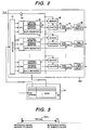
- Fig. 3 is an illustration of the Sync signal used in the exemplary electronic control unit for automobiles. Here, an example of a four-cylinder engine will be explained.
- a pulse signal indicating the reference position of a specific piston of each cylinder is outputted from the timer circuit 13 of the microcomputer 1.
- the pulse width of the reference signal of the first cylinder is made narrower than the pulse width of the reference signal of the third cylinder and the pulse width indicating the reference piston position is changed for each cylinder, even a driver IC having no CPU can discriminate the cylinder.
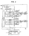
- Fig. 4 is a block diagram showing the constitution of the essential section of the driver IC 2B used in the exemplary electronic control unit for automobiles
- the timer circuit 20B for each of channels ch1, ch2, ---, has a control register 32, a pulse generation start register (PULSE#_S) 43, a pulse generation end register (PULSE#_E) 44, a register (Sync_PW#) 45 storing the Sync signal pulse width of each cylinder, the counter 35, the comparator 46 for resetting the counter 35, the divider 36, the comparator 37, and the pulse output circuit 38.
- PULSE#_S pulse generation start register
- PULSE#_E pulse generation end register
- Sync_PW# register
- the CLK signal passes the buffer 39 and the dividers 36 and 40 and is distributed to the counter 35 for generating a pulse signal and the counter 41 for measuring the Sync signal pulse width.
- the input capture register (ICR) 42 captures the value of the counter 41 at the edge of the Sync signal pulse.
- addresses are respectively assigned and the register designated by the microcomputer 1 is selected by the decoder 31.
- the microcomputer 1 transmits the address of the register to be accessed and the data to be written into the register as a frame and it is stored in the receiving buffer 24 of the serial communication interface 32.
- the division ratio of the divider 36 and the polarity of a pulse output signal are set. Further, in the PULSE#_S register 43 and the PULSE#_E register 44, the pulse generation timing and pulse end timing based on the Sync signal pulse are respectively set and in the Sync_PW# register 45, for each cylinder, the pulse width of the Sync signal corresponding to the cylinder is set.
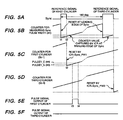
- Fig. 5 is a timing chart showing the generation operation of a pulse output signal by the timer circuit 20B of the exemplary electronic control unit for automobiles.
- the counter 41 for measuring the Sync pulse width counts up in synchronization with the divided clock signal. And, as shown in Fig. 5(B) , at the time t1, the counter is reset at the leading edge of the Sync signal. After reset, the counter starts count up again. And, as shown in Fig. 5(B) , at the time t2, the counter value at the point of time of the trailing edge of the Sync signal is captured by the ICR 42.
- the pulse generation counter 35 also counts up in synchronization with the divided clock signal. However, when the value captured by the ICR 42 is equal to the value written in the Sycn_PW of the same channel, as shown in Fig. 5(C) , at the time t2, the counter is reset at the trailing edge of the Sync signal.
- the pulse width of the reference signal of the first cylinder of the Sync signal coincides with the value of the Sync_PW1 of the channel 1, so that only the counter 35-1 of the channel 1 is reset at the trailing edge of the Sync signal.
- the counter 35-1 After reset, starts count up again, and at the time t3, when the value coincides with the value of the PULSE_S register 43, the port output is inverted from low to high, and as shown in Fig. 5(E) , pulse signal output is started.
- the control unit can respond to multi-stage of fuel injection and ignition.
- the ignition and fuel injection time based on a specific piston position and the pulse width can be freely controlled for each cylinder.
- a generation method of a pulse signal as mentioned above, not only a control data signal for setting the pulse signal output start timing and output end timing is used but also a control data signal for setting the pulse signal output start timing and pulse width may be used.
- the driver IC 2A has the timer circuit 20A and the driver IC 2B has the timer circuit 20B.
- both the driver ICs 2A and 2B can have both the timer circuits 20A and 20B.
- the driver ICs can be shared, so that the mass productivity is improved and an inexpensive constitution can be realized.
- either of the solenoid and relay driving timer function (20A) and the injector and igniter driving timer function (20B) can be selected.
- the timer circuits can be structured so as to select two functions for each channel.
- the number of timer ports of the microcomputer can be reduced, so that an inexpensive microcomputer having a smaller package can be used. Further, when the number of actuators to be controlled is increased, in a conventional system, the timer ports of the microcomputer are insufficient, so that the microcomputer must be graded up. However, in this example, there is no need to grade up the microcomputer and increase the number of wires, so that the control system can be expanded easily.
- the microcomputer supplies the clock signal to the driver ICs, thus the driver ICs themselves does not need to have an oscillator for timer count, so that the timer-built-in drivers IC can be produced at a low price.
- the microcomputer1 notifies the timer-built-in driver IC 2B of the piston reference position of each cylinder using the Sync signal, so that the driver ICs do not need to have a built-in CPU and the power transistors for driving the injector and igniter can be controlled from the microcomputer via the serial communication line. Therefore, the microcomputer does not need to individually control the power transistors in on and off, so that the number of wires between the microcomputer and the output driver circuit can be reduced greatly.
- the timer circuit may output only the Sync signal, thus the area thereof can be made smaller and the number of timer ports can be simultaneously reduced greatly, so that an inexpensive microcomputer having a smaller package can be used.
- Fig. 6 is a block diagram showing the whole constitution of the electronic control unit for automobiles of the first embodiment of the present invention. Further, the same numerals as those shown in Fig. 1 indicate the same parts.
- the differences from the constitution shown in Fig. 1 are a timer circuit 13A of a microcomputer 1A and a timer circuit 20C of a timer-built-in driver IC 2C.
- the crank angle sensor signal S1 and the cam angle sensor signal S2 are input to not only the timer circuit 13A of the microcomputer 1A but also the timer circuit 20C of the timer-built-in driver IC 2C for driving the injector A1 and the igniter A2.
- the timer circuit 20C is structured, on the basis of these sensor signals, so as to decide the piston reference position of each cylinder of the engine and output a pulse signal in synchronization with it. Therefore, unlike Fig. 1 , from the timer 13A of the microcomputer 1A, the Sync signal is not transmitted to the timer-built-in driver IC 2C.
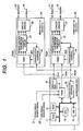
- Fig. 7 is a block diagram showing the constitution of the essential section of the driver IC 2C used in the electronic control unit for automobiles of the first embodiment of the present invention. Further, the same numerals as those shown in Fig. 4 indicate the same parts.
- an engine position decision circuit 47 for generating the Sync signal on the basis of the crank angle sensor signal S1 and the cam angle sensor signal S2 and a pulse pattern specification storage register 48 are added.
- the crank angle sensor signal S1 and the cam angle sensor signal S2 are input to the engine position decision circuit 47.
- the engine position decision circuit 47 generates the Sync signal by discriminating the piston position of each cylinder of the engine and supplies it to the counter 41 for measuring the Sync pulse width.
- the operations other than it are the same as those of the timer circuit 20B shown in Fig. 4 .
- the pulse patterns of the crank angle sensor and cam angle sensor depend on the engine, so that at the time of initialization, the microcomputer can set the pulse pattern specification of the engine to be controlled in the pulse pattern specification storage register 48.
- the number of timer ports of the microcomputer can be reduced, so that an inexpensive microcomputer having a smaller package can be used and there is no need to grade up the microcomputer and increase the number of wires, so that the control system can be expanded easily.
- the microcomputer supplies the clock signal to the driver ICs, thus the driver ICs themselves do not need to have an oscillator for timer count, so that a timer-built-in driver ICs can be produced at a low price.
- Fig. 8 is a block diagram showing the whole constitution of the another exemplary electronic control unit for automobiles. Further, the same numerals as those shown in Fig. 1 indicate the same parts.
- the difference from the constitution shown in Fig. 1 is input/output ICs 50A and 50B.
- the input/output ICs 50A and 50B are respectively the timer-built-in driver ICs 2A and 2B shown in Fig. 1 having the built-in A-D converter 14.
- Various sensor signals S are input to the A-D converters 14 of the input/output ICs 50A and 50B.
- the A-D conversion results are transmitted to the microcomputer 1A via the serial communication interfaces 23 and 15. Further, the clock signal CLK for timer count is supplied to the A-D converter 14.
- the A-D converts and A-D input ports of the microcomputer 1A can be reduced, so that the chip area and the number of ports of the microcomputer can be reduced more.
- the architecture of forming the microcomputer core such as the CPU and memory and the input/output circuit such as the timer and A-D converter in different chips an optimal semiconductor process can be applied to each chip.
- a finer process can be applied to the CPU core and memory than the process of a 1-chip microcomputer having a core and a peripheral input/output circuit which are integrated, so that the operation is speeded up and the control application program including the model base control can be executed at high speed.
- Fig. 9 is a block diagram showing the whole constitution of the further exemplary electronic control unit for automobiles invention. Further, the same numerals as those shown in Fig. 1 indicate the same parts.
- the difference from the constitution shown in Fig. 8 is a respect that an A-D conversion IC 51 is formed in a different chip from that of the output driver circuits 2A and 2B.
- the A-D conversion IC 51 is composed of the A-D converter 14 and a serial communication interface 52 and transmits A-D conversion values of various sensor signals S to a microcomputer 1D by serial communication.
- This constitution is suitable particularly when there is the possibility that electrical noise generated by the output driver circuits 2A and 2B supplying a large current may degrade the A-D conversion accuracy.
- the number of wires from the microcomputer to the driver ICs can be reduced and the actuators can be driven without the microcomputer being built in.
Landscapes
- Engineering & Computer Science (AREA)
- Chemical & Material Sciences (AREA)
- Combustion & Propulsion (AREA)
- Mechanical Engineering (AREA)
- General Engineering & Computer Science (AREA)
- Theoretical Computer Science (AREA)
- Signal Processing (AREA)
- Combined Controls Of Internal Combustion Engines (AREA)
- Arrangements For Transmission Of Measured Signals (AREA)
Claims (6)
- Unité de commande électronique pour une automobile comportant un micro-ordinateur (1, 1A) pour rendre opérationnel un signal de commande afin de commander un état d'une automobile sur la base d'un signal d'entrée (S1, S2) en provenance d'un capteur, un circuit d'attaque de sortie pour entraîner un actionneur (A1-A4) par l'intermédiaire dudit signal de commande obtenu par ledit micro-ordinateur (1, 1A),
caractérisé en ce que
ledit circuit d'attaque de sortie est un circuit à semi-conducteurs intégré comportant un circuit d'horloge intégré (20A-20C) pour générer un signal de modulation de largeur d'impulsion et un signal impulsionnel, un circuit d'attaque de sortie (22) étant constitué de transistors de puissance et d'une interface de communication série (23),
ledit circuit d'horloge (20A-20C), sur la base dudit signal de données de commande reçu en provenance dudit micro-ordinateur (1, 1A) par l'intermédiaire de ladite interface de communication série (23), générant ledit signal de modulation de largeur d'impulsion et ledit signal impulsionnel, ledit circuit d'horloge (20A, 20C) incluant en outre un circuit de détermination de position de moteur pour générer un signal de synchronisation sur la base d'un signal de détecteur d'angle de vilebrequin et d'un signal de détecteur d'angle de came et ledit circuit d'horloge (20A, 20C) incluant en outre un registre de mémorisation de spécification de modèle impulsionnel (48) de sorte qu'au moment de l'initialisation, le micro-ordinateur (1, 1A) peut établir la spécification de modèle impulsionnel du moteur à commander dans le registre de mémorisation de spécification de modèle impulsionnel (48). - Unité de commande électronique pour automobiles selon la revendication 1, dans laquelle
ledit micro-ordinateur (1, 1A) délivre un signal d'horloge pour un comptage d'horloge audit circuit d'horloge intégré dans ledit circuit intégré d'attaque (2A-2C). - Unité de commande électronique pour automobiles selon au moins l'une des revendications 1 à 2, dans laquelle ledit signal synchronisé de rotation de moteur est un signal impulsionnel indiquant que le piston de chaque cylindre dudit moteur est positionné à un point de référence spécifique et que la largeur d'impulsion dudit signal dépend du nombre de cylindres.
- Unité de commande électronique pour automobiles selon au moins l'une des revendications 1 à 3, dans laquelle
ledit circuit d'horloge (20A-20C), sur la base dudit signal de détecteur d'angle de vilebrequin et dudit signal de détecteur d'angle de came, lesquels sont entrés dans ledit circuit d'horloge (20A, 20C), discrimine la position de chaque cylindre dudit moteur. - Unité de commande électronique pour automobiles selon au moins l'une des revendications 1 à 4, dans laquelle ledit circuit intégré d'attaque (2A-2C) a en outre un convertisseur analogique/numérique (A/N) intégré, convertit un signal de détection en un signal numérique par l'intermédiaire dudit convertisseur A/N, et transmet un résultat de conversion audit micro-ordinateur (1, 1A) via ladite communication série.
- Unité de commande électronique pour automobiles selon au moins l'une des revendications 1 à 5, comportant en outre, en plus dudit circuit intégré d'attaque (2A-2C), un circuit intégré de conversion A/N constitué d'un convertisseur A/N et d'une interface de communication série (23), un résultat de conversion A/N par l'intermédiaire dudit convertisseur A/N étant transmis audit micro-ordinateur (1-1A) via ladite communication série.
Applications Claiming Priority (2)
| Application Number | Priority Date | Filing Date | Title |
|---|---|---|---|
| JP2003135632A JP4449029B2 (ja) | 2003-05-14 | 2003-05-14 | 自動車用電子制御装置及びそれに用いる出力ドライバ回路 |
| JP2003135632 | 2003-05-14 |
Publications (3)
| Publication Number | Publication Date |
|---|---|
| EP1477656A2 EP1477656A2 (fr) | 2004-11-17 |
| EP1477656A3 EP1477656A3 (fr) | 2006-11-22 |
| EP1477656B1 true EP1477656B1 (fr) | 2011-05-11 |
Family
ID=33028361
Family Applications (1)
| Application Number | Title | Priority Date | Filing Date |
|---|---|---|---|
| EP04006702A Expired - Lifetime EP1477656B1 (fr) | 2003-05-14 | 2004-03-19 | Unité de commande électronique pour automobiles et circuit d'attaque de sortie correspondant |
Country Status (3)
| Country | Link |
|---|---|
| US (1) | US7509206B2 (fr) |
| EP (1) | EP1477656B1 (fr) |
| JP (1) | JP4449029B2 (fr) |
Families Citing this family (25)
| Publication number | Priority date | Publication date | Assignee | Title |
|---|---|---|---|---|
| US7362152B2 (en) * | 2004-03-24 | 2008-04-22 | Texas Instruments Incorporated | Apparatus and method for digital phase control of a pulse width modulation generator for microprocessor/DSP in integrated circuits |
| US7502963B2 (en) * | 2005-02-20 | 2009-03-10 | Delphi Technologies, Inc. | Optimization by using output drivers for discrete input interface |
| DE102005051423B3 (de) * | 2005-10-27 | 2007-03-08 | Keiper Gmbh & Co.Kg | Crashaktive Kopfstütze |
| US8078339B2 (en) * | 2007-07-13 | 2011-12-13 | Cummins Inc. | Circuit board with integrated connector |
| US8560124B2 (en) | 2007-07-13 | 2013-10-15 | Cummins Inc. | Idle control system and method for adaptive temperature control |
| JP4469886B2 (ja) * | 2007-09-20 | 2010-06-02 | 日立オートモティブシステムズ株式会社 | 負荷駆動回路 |
| JP5331730B2 (ja) * | 2010-02-24 | 2013-10-30 | 日立オートモティブシステムズ株式会社 | 内燃機関制御装置 |
| EP2583471B1 (fr) * | 2010-06-15 | 2019-08-07 | Continental Teves AG & Co. OHG | Procédé de synchronisation de capteurs |
| JP5722150B2 (ja) * | 2011-07-21 | 2015-05-20 | ルネサスエレクトロニクス株式会社 | マイクロコントローラ |
| JP5659117B2 (ja) * | 2011-09-20 | 2015-01-28 | 日立オートモティブシステムズ株式会社 | 内燃機関の燃料噴射装置 |
| JP5451705B2 (ja) | 2011-09-21 | 2014-03-26 | 日立オートモティブシステムズ株式会社 | 自動車用電子制御装置及びデータ通信方法 |
| JP5392337B2 (ja) * | 2011-10-18 | 2014-01-22 | 株式会社デンソー | センサ信号の処理装置 |
| JP5852914B2 (ja) * | 2012-03-30 | 2016-02-03 | 日立オートモティブシステムズ株式会社 | 電子制御装置 |
| JP5948230B2 (ja) | 2012-11-26 | 2016-07-06 | 日立オートモティブシステムズ株式会社 | 車載制御装置 |
| US9989947B2 (en) * | 2013-08-20 | 2018-06-05 | Infineon Technologies Ag | Driver circuit for driving electromagnetic actuators |
| JP6416607B2 (ja) * | 2014-12-10 | 2018-10-31 | 日立オートモティブシステムズ株式会社 | 電子制御装置 |
| US10087872B2 (en) * | 2015-11-18 | 2018-10-02 | Infineon Technologies Ag | System and method for a synchronized driver circuit |
| US10184860B2 (en) | 2016-04-08 | 2019-01-22 | Infineon Technologies Ag | Control system for power train control |
| US11079730B2 (en) | 2016-12-05 | 2021-08-03 | Hitachi Automotive Systems, Ltd. | Control device comprising a processor and an IC |
| JP6871073B2 (ja) | 2017-06-08 | 2021-05-12 | 日立Astemo株式会社 | 電子制御装置 |
| US10129339B1 (en) | 2017-11-15 | 2018-11-13 | Sensata Technologies, Inc. | Communication system configured for transmitting sensor values from N sensing sources to a control unit |
| KR102085896B1 (ko) | 2018-12-07 | 2020-03-06 | 현대오트론 주식회사 | 파워트레인 엔진 정밀 제어방법 및 이에 의해 운용되는 자동차 |
| JP7626364B2 (ja) * | 2020-08-18 | 2025-02-04 | 株式会社デンソー | 負荷駆動システム |
| CN114779699B (zh) * | 2022-04-27 | 2025-12-30 | 凌云天博光电科技股份有限公司 | 一种频闪型控制器及其输出控制方法 |
| US12038783B1 (en) * | 2023-02-08 | 2024-07-16 | GM Global Technology Operations LLC | System and method for fault tolerant time synchronization |
Family Cites Families (13)
| Publication number | Priority date | Publication date | Assignee | Title |
|---|---|---|---|---|
| JPH0833143B2 (ja) * | 1987-02-23 | 1996-03-29 | 三菱電機株式会社 | エンジンの制御装置 |
| US4989150A (en) * | 1990-02-23 | 1991-01-29 | Fuji Jukogyo Kabushiki Kaisha | Injector diagnosis system |
| KR950009974B1 (ko) | 1991-06-27 | 1995-09-04 | 미쓰비시덴키가부시키가이샤 | 내연기관 점화제어장치 |
| US5263460A (en) * | 1992-04-30 | 1993-11-23 | Chrysler Corporation | Duty cycle purge control system |
| SE503397C2 (sv) | 1994-09-11 | 1996-06-03 | Mecel Ab | Arrangemang och förfarande för ett reglersystem till en förbränningsmotor innefattande ett distribuerat datornät |
| JPH09154181A (ja) | 1995-11-30 | 1997-06-10 | Mitsubishi Electric Corp | 自動車総合制御装置 |
| DE19610609B4 (de) | 1996-03-18 | 2004-01-29 | Robert Bosch Gmbh | Anordnung zum Steuern sich zyklisch wiederholender Vorgänge in Brennkraftmaschinen |
| FR2776413B1 (fr) | 1998-03-17 | 2000-05-26 | Renault | Systeme de generation de commandes d'actionneurs |
| JP3692820B2 (ja) | 1999-03-10 | 2005-09-07 | 株式会社デンソー | 自動車用制御装置 |
| US6560528B1 (en) * | 2000-03-24 | 2003-05-06 | Internal Combustion Technologies, Inc. | Programmable internal combustion engine controller |
| JP4253110B2 (ja) * | 2000-09-04 | 2009-04-08 | 株式会社日立製作所 | 車両制御システム |
| JP3970196B2 (ja) * | 2003-03-19 | 2007-09-05 | 三菱電機株式会社 | エンジン用吸気量制御装置及びエンジン用吸気量制御方法 |
| US7126463B2 (en) * | 2003-08-01 | 2006-10-24 | General Motors Corporation | PWM and variable frequency based position indicators |
-
2003
- 2003-05-14 JP JP2003135632A patent/JP4449029B2/ja not_active Expired - Fee Related
-
2004
- 2004-03-17 US US10/801,859 patent/US7509206B2/en not_active Expired - Fee Related
- 2004-03-19 EP EP04006702A patent/EP1477656B1/fr not_active Expired - Lifetime
Also Published As
| Publication number | Publication date |
|---|---|
| JP2004339977A (ja) | 2004-12-02 |
| EP1477656A3 (fr) | 2006-11-22 |
| US20040230347A1 (en) | 2004-11-18 |
| US7509206B2 (en) | 2009-03-24 |
| JP4449029B2 (ja) | 2010-04-14 |
| EP1477656A2 (fr) | 2004-11-17 |
Similar Documents
| Publication | Publication Date | Title |
|---|---|---|
| EP1477656B1 (fr) | Unité de commande électronique pour automobiles et circuit d'attaque de sortie correspondant | |
| US5778858A (en) | Fuel injection split engine | |
| WO1998027327A9 (fr) | Moteur a injection a fonctionnement fractionne | |
| GB2216292A (en) | Diagnostic system for the electronic control system of an automotive engine | |
| EP0740059B1 (fr) | Appareil pour commander un convertisseur analogique-numérique destiné à un moteur à combustion interne | |
| US8156269B2 (en) | Reference distribution bus | |
| CN101243363B (zh) | 提供控制设备的基本功能性的控制芯片 | |
| JP5331730B2 (ja) | 内燃機関制御装置 | |
| US5734920A (en) | Input/output processing IC | |
| US7079934B2 (en) | Set of peripheral chips | |
| US8010722B2 (en) | Analog comparators in a control system | |
| JP3925196B2 (ja) | 車両用電子機器 | |
| US20050278081A1 (en) | Expandable control unit | |
| US7308595B2 (en) | Method and device for generating an internal time base for a diagnostic function for an output module | |
| US5295471A (en) | Electronic engine control interface | |
| US7920954B2 (en) | Method and system for multi-purposely controlling an internal-combustion engine on an engine bench testing unit | |
| US4855919A (en) | Method and circuitry for the driving of driver stages for functions of internal combustion engines for automotive vehicles especially for fuel injection or ignition | |
| US8417857B2 (en) | Digital I/O signal scheduler | |
| US7367321B2 (en) | Erroneous connection detecting method of ignition devices and apparatus of the same | |
| US20030056762A1 (en) | Method and arrangement for monitoring the drive of an actuator | |
| JPH04232555A (ja) | タイマ・システム | |
| JP2612636B2 (ja) | 入出力ターミナルユニット | |
| JP2020013177A (ja) | 電子制御装置 | |
| KR19980026413A (ko) | 직렬 통신 포트 다중화 제어장치 및 그 방법 | |
| JP2007088759A (ja) | ワンショットパルス発生回路 |
Legal Events
| Date | Code | Title | Description |
|---|---|---|---|
| PUAI | Public reference made under article 153(3) epc to a published international application that has entered the european phase |
Free format text: ORIGINAL CODE: 0009012 |
|
| AK | Designated contracting states |
Kind code of ref document: A2 Designated state(s): AT BE BG CH CY CZ DE DK EE ES FI FR GB GR HU IE IT LI LU MC NL PL PT RO SE SI SK TR |
|
| AX | Request for extension of the european patent |
Extension state: AL LT LV MK |
|
| RIN1 | Information on inventor provided before grant (corrected) |
Inventor name: SASAKI, SHOJIHITACHI, LTD.INT. PROP GROUP Inventor name: KANEKAWA, NOBUYASUHITACHI, LTD.INT. PROP GROUP Inventor name: SAKURAI, KOHEIHITACHI, LTD.INT. PROPERTY GROUP |
|
| PUAL | Search report despatched |
Free format text: ORIGINAL CODE: 0009013 |
|
| AK | Designated contracting states |
Kind code of ref document: A3 Designated state(s): AT BE BG CH CY CZ DE DK EE ES FI FR GB GR HU IE IT LI LU MC NL PL PT RO SE SI SK TR |
|
| AX | Request for extension of the european patent |
Extension state: AL LT LV MK |
|
| 17P | Request for examination filed |
Effective date: 20070522 |
|
| AKX | Designation fees paid |
Designated state(s): DE |
|
| 17Q | First examination report despatched |
Effective date: 20070820 |
|
| GRAP | Despatch of communication of intention to grant a patent |
Free format text: ORIGINAL CODE: EPIDOSNIGR1 |
|
| GRAS | Grant fee paid |
Free format text: ORIGINAL CODE: EPIDOSNIGR3 |
|
| GRAA | (expected) grant |
Free format text: ORIGINAL CODE: 0009210 |
|
| RAP1 | Party data changed (applicant data changed or rights of an application transferred) |
Owner name: HITACHI, LTD. |
|
| AK | Designated contracting states |
Kind code of ref document: B1 Designated state(s): DE |
|
| REG | Reference to a national code |
Ref country code: DE Ref legal event code: R096 Ref document number: 602004032593 Country of ref document: DE Effective date: 20110622 |
|
| PLBE | No opposition filed within time limit |
Free format text: ORIGINAL CODE: 0009261 |
|
| STAA | Information on the status of an ep patent application or granted ep patent |
Free format text: STATUS: NO OPPOSITION FILED WITHIN TIME LIMIT |
|
| 26N | No opposition filed |
Effective date: 20120214 |
|
| REG | Reference to a national code |
Ref country code: DE Ref legal event code: R097 Ref document number: 602004032593 Country of ref document: DE Effective date: 20120214 |
|
| PGFP | Annual fee paid to national office [announced via postgrant information from national office to epo] |
Ref country code: DE Payment date: 20160315 Year of fee payment: 13 |
|
| REG | Reference to a national code |
Ref country code: DE Ref legal event code: R119 Ref document number: 602004032593 Country of ref document: DE |
|
| PG25 | Lapsed in a contracting state [announced via postgrant information from national office to epo] |
Ref country code: DE Free format text: LAPSE BECAUSE OF NON-PAYMENT OF DUE FEES Effective date: 20171003 |