EP1477860A1 - Zur Herstellung eines mikroelektronischen Elements geeignete Struktur einer lithographischen Marke - Google Patents
Zur Herstellung eines mikroelektronischen Elements geeignete Struktur einer lithographischen Marke Download PDFInfo
- Publication number
- EP1477860A1 EP1477860A1 EP03076422A EP03076422A EP1477860A1 EP 1477860 A1 EP1477860 A1 EP 1477860A1 EP 03076422 A EP03076422 A EP 03076422A EP 03076422 A EP03076422 A EP 03076422A EP 1477860 A1 EP1477860 A1 EP 1477860A1
- Authority
- EP
- European Patent Office
- Prior art keywords
- marker
- ordering
- substrate
- structural elements
- structural element
- Prior art date
- Legal status (The legal status is an assumption and is not a legal conclusion. Google has not performed a legal analysis and makes no representation as to the accuracy of the status listed.)
- Withdrawn
Links
- 239000003550 marker Substances 0.000 title claims abstract description 225
- 238000012545 processing Methods 0.000 title claims description 36
- 238000004377 microelectronic Methods 0.000 title claims description 6
- 239000000758 substrate Substances 0.000 claims abstract description 82
- 230000003287 optical effect Effects 0.000 claims abstract description 67
- 238000000034 method Methods 0.000 claims abstract description 43
- 230000008569 process Effects 0.000 claims abstract description 33
- 238000005259 measurement Methods 0.000 claims abstract description 18
- 230000003252 repetitive effect Effects 0.000 claims abstract description 16
- 230000000737 periodic effect Effects 0.000 claims description 56
- 239000000463 material Substances 0.000 claims description 40
- 230000005855 radiation Effects 0.000 claims description 26
- 229910052751 metal Inorganic materials 0.000 claims description 24
- 239000002184 metal Substances 0.000 claims description 24
- 238000001465 metallisation Methods 0.000 claims description 22
- 230000000295 complement effect Effects 0.000 claims description 15
- 238000000059 patterning Methods 0.000 claims description 14
- 239000004065 semiconductor Substances 0.000 claims description 14
- 238000005498 polishing Methods 0.000 claims description 10
- 239000010949 copper Substances 0.000 claims description 9
- 239000012212 insulator Substances 0.000 claims description 7
- 239000003989 dielectric material Substances 0.000 claims description 5
- 239000000126 substance Substances 0.000 claims description 5
- 230000002441 reversible effect Effects 0.000 claims description 4
- RYGMFSIKBFXOCR-UHFFFAOYSA-N Copper Chemical compound [Cu] RYGMFSIKBFXOCR-UHFFFAOYSA-N 0.000 claims description 3
- 238000000151 deposition Methods 0.000 claims 3
- 230000008021 deposition Effects 0.000 claims 3
- 229910052802 copper Inorganic materials 0.000 claims 2
- 239000004411 aluminium Substances 0.000 claims 1
- 229910052782 aluminium Inorganic materials 0.000 claims 1
- XAGFODPZIPBFFR-UHFFFAOYSA-N aluminium Chemical compound [Al] XAGFODPZIPBFFR-UHFFFAOYSA-N 0.000 claims 1
- 239000004020 conductor Substances 0.000 claims 1
- 238000002161 passivation Methods 0.000 claims 1
- 239000010410 layer Substances 0.000 description 63
- VYPSYNLAJGMNEJ-UHFFFAOYSA-N Silicium dioxide Chemical compound O=[Si]=O VYPSYNLAJGMNEJ-UHFFFAOYSA-N 0.000 description 32
- WFKWXMTUELFFGS-UHFFFAOYSA-N tungsten Chemical compound [W] WFKWXMTUELFFGS-UHFFFAOYSA-N 0.000 description 29
- 239000010937 tungsten Substances 0.000 description 22
- 229910052721 tungsten Inorganic materials 0.000 description 21
- 235000012239 silicon dioxide Nutrition 0.000 description 16
- 239000000377 silicon dioxide Substances 0.000 description 16
- 230000000694 effects Effects 0.000 description 12
- 238000004519 manufacturing process Methods 0.000 description 11
- 230000008859 change Effects 0.000 description 10
- 230000006870 function Effects 0.000 description 8
- 230000004048 modification Effects 0.000 description 7
- 238000012986 modification Methods 0.000 description 7
- 230000002411 adverse Effects 0.000 description 4
- 230000008033 biological extinction Effects 0.000 description 4
- 230000005540 biological transmission Effects 0.000 description 4
- 238000001514 detection method Methods 0.000 description 3
- 238000009826 distribution Methods 0.000 description 3
- 238000007667 floating Methods 0.000 description 3
- XUIMIQQOPSSXEZ-UHFFFAOYSA-N Silicon Chemical compound [Si] XUIMIQQOPSSXEZ-UHFFFAOYSA-N 0.000 description 2
- 238000003491 array Methods 0.000 description 2
- 230000006399 behavior Effects 0.000 description 2
- 238000005234 chemical deposition Methods 0.000 description 2
- 238000006243 chemical reaction Methods 0.000 description 2
- 238000010276 construction Methods 0.000 description 2
- 238000013461 design Methods 0.000 description 2
- 238000005530 etching Methods 0.000 description 2
- 238000003384 imaging method Methods 0.000 description 2
- 239000011159 matrix material Substances 0.000 description 2
- QSHDDOUJBYECFT-UHFFFAOYSA-N mercury Chemical compound [Hg] QSHDDOUJBYECFT-UHFFFAOYSA-N 0.000 description 2
- 229910052753 mercury Inorganic materials 0.000 description 2
- 230000006911 nucleation Effects 0.000 description 2
- 238000010899 nucleation Methods 0.000 description 2
- 230000010363 phase shift Effects 0.000 description 2
- 238000001020 plasma etching Methods 0.000 description 2
- 238000002310 reflectometry Methods 0.000 description 2
- 230000004044 response Effects 0.000 description 2
- 229910052710 silicon Inorganic materials 0.000 description 2
- 239000010703 silicon Substances 0.000 description 2
- 238000001228 spectrum Methods 0.000 description 2
- 238000012876 topography Methods 0.000 description 2
- 238000001429 visible spectrum Methods 0.000 description 2
- XOJVVFBFDXDTEG-UHFFFAOYSA-N Norphytane Natural products CC(C)CCCC(C)CCCC(C)CCCC(C)C XOJVVFBFDXDTEG-UHFFFAOYSA-N 0.000 description 1
- 238000000637 aluminium metallisation Methods 0.000 description 1
- 238000000137 annealing Methods 0.000 description 1
- 230000002238 attenuated effect Effects 0.000 description 1
- 230000004888 barrier function Effects 0.000 description 1
- 230000008901 benefit Effects 0.000 description 1
- 239000011248 coating agent Substances 0.000 description 1
- 238000000576 coating method Methods 0.000 description 1
- 230000003750 conditioning effect Effects 0.000 description 1
- 238000005137 deposition process Methods 0.000 description 1
- 238000011161 development Methods 0.000 description 1
- 230000018109 developmental process Effects 0.000 description 1
- 230000009977 dual effect Effects 0.000 description 1
- 230000005684 electric field Effects 0.000 description 1
- 230000005670 electromagnetic radiation Effects 0.000 description 1
- 238000005516 engineering process Methods 0.000 description 1
- 238000005286 illumination Methods 0.000 description 1
- 238000007689 inspection Methods 0.000 description 1
- 230000003993 interaction Effects 0.000 description 1
- 238000005468 ion implantation Methods 0.000 description 1
- 239000002346 layers by function Substances 0.000 description 1
- 239000004973 liquid crystal related substance Substances 0.000 description 1
- 238000001459 lithography Methods 0.000 description 1
- 230000005381 magnetic domain Effects 0.000 description 1
- 230000015654 memory Effects 0.000 description 1
- 238000012544 monitoring process Methods 0.000 description 1
- 230000000877 morphologic effect Effects 0.000 description 1
- 230000003647 oxidation Effects 0.000 description 1
- 238000007254 oxidation reaction Methods 0.000 description 1
- 238000005240 physical vapour deposition Methods 0.000 description 1
- 238000007517 polishing process Methods 0.000 description 1
- 230000037452 priming Effects 0.000 description 1
- 230000011218 segmentation Effects 0.000 description 1
- 238000007493 shaping process Methods 0.000 description 1
- 239000010409 thin film Substances 0.000 description 1
- 238000011282 treatment Methods 0.000 description 1
- DZKDPOPGYFUOGI-UHFFFAOYSA-N tungsten dioxide Inorganic materials O=[W]=O DZKDPOPGYFUOGI-UHFFFAOYSA-N 0.000 description 1
Images



Classifications
-
- G—PHYSICS
- G03—PHOTOGRAPHY; CINEMATOGRAPHY; ANALOGOUS TECHNIQUES USING WAVES OTHER THAN OPTICAL WAVES; ELECTROGRAPHY; HOLOGRAPHY
- G03F—PHOTOMECHANICAL PRODUCTION OF TEXTURED OR PATTERNED SURFACES, e.g. FOR PRINTING, FOR PROCESSING OF SEMICONDUCTOR DEVICES; MATERIALS THEREFOR; ORIGINALS THEREFOR; APPARATUS SPECIALLY ADAPTED THEREFOR
- G03F9/00—Registration or positioning of originals, masks, frames, photographic sheets or textured or patterned surfaces, e.g. automatically
- G03F9/70—Registration or positioning of originals, masks, frames, photographic sheets or textured or patterned surfaces, e.g. automatically for microlithography
- G03F9/7088—Alignment mark detection, e.g. TTR, TTL, off-axis detection, array detector, video detection
-
- G—PHYSICS
- G03—PHOTOGRAPHY; CINEMATOGRAPHY; ANALOGOUS TECHNIQUES USING WAVES OTHER THAN OPTICAL WAVES; ELECTROGRAPHY; HOLOGRAPHY
- G03F—PHOTOMECHANICAL PRODUCTION OF TEXTURED OR PATTERNED SURFACES, e.g. FOR PRINTING, FOR PROCESSING OF SEMICONDUCTOR DEVICES; MATERIALS THEREFOR; ORIGINALS THEREFOR; APPARATUS SPECIALLY ADAPTED THEREFOR
- G03F7/00—Photomechanical, e.g. photolithographic, production of textured or patterned surfaces, e.g. printing surfaces; Materials therefor, e.g. comprising photoresists; Apparatus specially adapted therefor
- G03F7/70—Microphotolithographic exposure; Apparatus therefor
- G03F7/70483—Information management; Active and passive control; Testing; Wafer monitoring, e.g. pattern monitoring
- G03F7/70605—Workpiece metrology
- G03F7/70616—Monitoring the printed patterns
-
- G—PHYSICS
- G03—PHOTOGRAPHY; CINEMATOGRAPHY; ANALOGOUS TECHNIQUES USING WAVES OTHER THAN OPTICAL WAVES; ELECTROGRAPHY; HOLOGRAPHY
- G03F—PHOTOMECHANICAL PRODUCTION OF TEXTURED OR PATTERNED SURFACES, e.g. FOR PRINTING, FOR PROCESSING OF SEMICONDUCTOR DEVICES; MATERIALS THEREFOR; ORIGINALS THEREFOR; APPARATUS SPECIALLY ADAPTED THEREFOR
- G03F7/00—Photomechanical, e.g. photolithographic, production of textured or patterned surfaces, e.g. printing surfaces; Materials therefor, e.g. comprising photoresists; Apparatus specially adapted therefor
- G03F7/70—Microphotolithographic exposure; Apparatus therefor
- G03F7/70483—Information management; Active and passive control; Testing; Wafer monitoring, e.g. pattern monitoring
- G03F7/70605—Workpiece metrology
- G03F7/70616—Monitoring the printed patterns
- G03F7/70625—Dimensions, e.g. line width, critical dimension [CD], profile, sidewall angle or edge roughness
-
- G—PHYSICS
- G03—PHOTOGRAPHY; CINEMATOGRAPHY; ANALOGOUS TECHNIQUES USING WAVES OTHER THAN OPTICAL WAVES; ELECTROGRAPHY; HOLOGRAPHY
- G03F—PHOTOMECHANICAL PRODUCTION OF TEXTURED OR PATTERNED SURFACES, e.g. FOR PRINTING, FOR PROCESSING OF SEMICONDUCTOR DEVICES; MATERIALS THEREFOR; ORIGINALS THEREFOR; APPARATUS SPECIALLY ADAPTED THEREFOR
- G03F7/00—Photomechanical, e.g. photolithographic, production of textured or patterned surfaces, e.g. printing surfaces; Materials therefor, e.g. comprising photoresists; Apparatus specially adapted therefor
- G03F7/70—Microphotolithographic exposure; Apparatus therefor
- G03F7/70483—Information management; Active and passive control; Testing; Wafer monitoring, e.g. pattern monitoring
- G03F7/70605—Workpiece metrology
- G03F7/70616—Monitoring the printed patterns
- G03F7/70633—Overlay, i.e. relative alignment between patterns printed by separate exposures in different layers, or in the same layer in multiple exposures or stitching
-
- G—PHYSICS
- G03—PHOTOGRAPHY; CINEMATOGRAPHY; ANALOGOUS TECHNIQUES USING WAVES OTHER THAN OPTICAL WAVES; ELECTROGRAPHY; HOLOGRAPHY
- G03F—PHOTOMECHANICAL PRODUCTION OF TEXTURED OR PATTERNED SURFACES, e.g. FOR PRINTING, FOR PROCESSING OF SEMICONDUCTOR DEVICES; MATERIALS THEREFOR; ORIGINALS THEREFOR; APPARATUS SPECIALLY ADAPTED THEREFOR
- G03F9/00—Registration or positioning of originals, masks, frames, photographic sheets or textured or patterned surfaces, e.g. automatically
- G03F9/70—Registration or positioning of originals, masks, frames, photographic sheets or textured or patterned surfaces, e.g. automatically for microlithography
- G03F9/7003—Alignment type or strategy, e.g. leveling, global alignment
- G03F9/7046—Strategy, e.g. mark, sensor or wavelength selection
-
- G—PHYSICS
- G03—PHOTOGRAPHY; CINEMATOGRAPHY; ANALOGOUS TECHNIQUES USING WAVES OTHER THAN OPTICAL WAVES; ELECTROGRAPHY; HOLOGRAPHY
- G03F—PHOTOMECHANICAL PRODUCTION OF TEXTURED OR PATTERNED SURFACES, e.g. FOR PRINTING, FOR PROCESSING OF SEMICONDUCTOR DEVICES; MATERIALS THEREFOR; ORIGINALS THEREFOR; APPARATUS SPECIALLY ADAPTED THEREFOR
- G03F9/00—Registration or positioning of originals, masks, frames, photographic sheets or textured or patterned surfaces, e.g. automatically
- G03F9/70—Registration or positioning of originals, masks, frames, photographic sheets or textured or patterned surfaces, e.g. automatically for microlithography
- G03F9/7073—Alignment marks and their environment
- G03F9/7076—Mark details, e.g. phase grating mark, temporary mark
-
- G—PHYSICS
- G03—PHOTOGRAPHY; CINEMATOGRAPHY; ANALOGOUS TECHNIQUES USING WAVES OTHER THAN OPTICAL WAVES; ELECTROGRAPHY; HOLOGRAPHY
- G03F—PHOTOMECHANICAL PRODUCTION OF TEXTURED OR PATTERNED SURFACES, e.g. FOR PRINTING, FOR PROCESSING OF SEMICONDUCTOR DEVICES; MATERIALS THEREFOR; ORIGINALS THEREFOR; APPARATUS SPECIALLY ADAPTED THEREFOR
- G03F9/00—Registration or positioning of originals, masks, frames, photographic sheets or textured or patterned surfaces, e.g. automatically
- G03F9/70—Registration or positioning of originals, masks, frames, photographic sheets or textured or patterned surfaces, e.g. automatically for microlithography
- G03F9/7073—Alignment marks and their environment
- G03F9/7084—Position of mark on substrate, i.e. position in (x, y, z) of mark, e.g. buried or resist covered mark, mark on rearside, at the substrate edge, in the circuit area, latent image mark, marks in plural levels
-
- G—PHYSICS
- G03—PHOTOGRAPHY; CINEMATOGRAPHY; ANALOGOUS TECHNIQUES USING WAVES OTHER THAN OPTICAL WAVES; ELECTROGRAPHY; HOLOGRAPHY
- G03F—PHOTOMECHANICAL PRODUCTION OF TEXTURED OR PATTERNED SURFACES, e.g. FOR PRINTING, FOR PROCESSING OF SEMICONDUCTOR DEVICES; MATERIALS THEREFOR; ORIGINALS THEREFOR; APPARATUS SPECIALLY ADAPTED THEREFOR
- G03F9/00—Registration or positioning of originals, masks, frames, photographic sheets or textured or patterned surfaces, e.g. automatically
- G03F9/70—Registration or positioning of originals, masks, frames, photographic sheets or textured or patterned surfaces, e.g. automatically for microlithography
- G03F9/7092—Signal processing
Definitions
- the present invention relates to a marker structure as defined in the preamble of claim 1.
- the present invention also relates to a lithographic projection apparatus comprising a device for wafer alignment which uses a marker structure as defined in the preamble of claim 27.
- the present invention relates to a method for wafer alignment using a marker structure as defined in the preamble of claim 28.
- the present invention finds an application in the field of lithographic projection apparatus that encompass a radiation system for supplying a proj ection beam of radiation, a support structure for supporting patterning means, which serves to pattern the projection beam according to a desired pattern, a substrate table for holding a substrate; and, a projection system for projecting the patterned beam onto a target portion of the substrate.
- patterning means as employed here should be broadly interpreted as referring to means that can be used to endow an incoming radiation beam with a patterned cross-section, corresponding to a pattern that is to be created in a target portion of the substrate; the term “light valve” can also be used in this context.
- the said pattern will correspond to a particular functional layer in a device being created in the target portion, such as an integrated circuit or other device (see below). Examples of such patterning means include:
- Lithographic projection apparatus can be used, for example, in the manufacture of integrated circuits (ICs).
- the patterning means may generate a circuit pattern corresponding to an individual layer of the IC, and this pattern can be imaged onto a target portion (e.g. comprising one or more dies) on a substrate (silicon wafer) that has been coated with a layer of radiation-sensitive material (resist).
- a target portion e.g. comprising one or more dies
- a substrate silicon wafer
- a layer of radiation-sensitive material resist
- a single wafer will contain a whole network of adjacent target portions that are successively irradiated via the projection system, one at a time.
- employing patterning by a mask on a mask table a distinction can be made between two different types of machine.
- each target portion is irradiated by exposing the entire mask pattern onto the target portion in one go; such an apparatus is commonly referred to as a wafer stepper or step-and-repeat apparatus.
- each target portion is irradiated by progressively scanning the mask pattern under the projection beam in a given reference direction (the "scanning" direction) while synchronously scanning the substrate table parallel or anti-parallel to this direction; since, in general, the projection system will have a magnification factor M (generally ⁇ 1), the speed V at which the substrate table is scanned will be a factor M times that at which the mask table is scanned.
- M magnification factor
- a pattern (e.g. in a mask) is imaged onto a substrate that is at least partially covered by a layer of radiation-sensitive material (resist).
- the substrate Prior to this imaging step, the substrate may undergo various procedures, such as priming, resist coating and a soft bake. After exposure, the substrate may be subjected to other procedures, such as a post-exposure bake (PEB), development, a hard bake and measurement/inspection of the imaged features.
- PEB post-exposure bake
- This array of procedures is used as a basis to pattern an individual layer of a device, e.g. an IC.
- Such a patterned layer may then undergo various processes such as etching, ion-implantation (doping), metallisation, oxidation, chemical-mechanical polishing, etc., all intended to finish off an individual layer. If several layers are required, then the whole procedure, or a variant thereof, will have to be repeated for each new layer. Eventually, an array of devices will be present on the substrate (wafer). These devices are then separated from one another by a technique such as dicing or sawing, whence the individual devices can be mounted on a carrier, connected to pins, etc.
- the projection system may hereinafter be referred to as the "lens"; however, this term should be broadly interpreted as encompassing various types of projection system, including refractive optics, reflective optics, and catadioptric systems, for example.
- the radiation system may also include components operating according to any of these design types for directing, shaping or controlling the projection beam of radiation, and such components may also be referred to below, collectively or singularly, as a "lens".
- the lithographic apparatus may be of a type having two or more substrate tables (and/or two or more mask tables). In such "multiple stage" devices the additional tables may be used in parallel, or preparatory steps may be carried out on one or more tables while one or more other tables are being used for exposures. Dual stage lithographic apparatus are described, for example, in US 5,969,441 and WO 98/40791, both incorporated herein by reference.
- the lithographic projection apparatus comprises a wafer alignment module which provides for alignment of the substrate with the mask and mask pattern within a given (specified) tolerance.
- the wafer alignment system typically performs the alignment based on optical means.
- the position of a wafer or a portion of a wafer is determined by measuring an optical response from an optical marker which is illuminated by an optical source: for example, a grating is illuminated by a laser beam, the laser beam diffracts from the grating, and one or more of the diffracted orders are measured by respective sensors, which are typically located on a reference plane. Using the output of the sensors the position of the wafer can be derived (relative to the reference plane).
- optical markers comprise a grating with a periodicity suitable for diffraction of impinging light with a wavelength well within the visible range of the spectrum.
- a typical periodicity is 16 ⁇ m.
- the grating is typically constructed of lines and trenches. Typically, the line width and trench width are each 8 ⁇ m.
- the grating In order to obtain sufficient diffracted light from the grating and to obtain well-defined diffraction maxima and minima, the grating must encompass a minimal number of lines and intermediate trenches.
- the size in the direction of the periodic structure is about 750 ⁇ m.
- the grating may be a phase grating or phase marker which takes into account a phase difference between the phase of rays scattered at the upper surface of the grating and the phase of rays scattered at the lower surface of the grating.
- the grating may be an amplitude grating which only takes into account the periodic structure of the grating without any further phase difference relating to an upper or lower level in the grating.
- an amplitude grating or amplitude marker is constructed of a periodic structure of first and second elements, which have similar surface levels but different respective reflectance.
- Optical markers are used during microelectronic device processing (or IC processing) along the full manufacturing line.
- FEOL front end of line
- BEOL back end of line
- markers are needed for alignment of metallisation structures, e.g. connect lines, and vias. It is noted that in both cases the integrity of the markers must be sufficient to meet the required accuracy of alignment.
- a wafer is subjected to a plurality of treatments such as annealing, etching, polishing, etc., which may likely cause roughness of a marker (a recessed area in the marker and/or warping of the marker).
- a marker a recessed area in the marker and/or warping of the marker.
- Such marker roughness causes an alignment error of the image which may contribute to an overlay error in the construction of a semiconductor device.
- phase depth can be defined as the resolved height difference between a top surface of a line and a top surface of a trench in a grating under a given angle of diffraction. If under an angle of diffraction, where (under optimal conditions) a maximum of diffracted intensity is expected, the phase depth equals half a wavelength of the applied radiation, interference between diffracted waves will result in a low or zero intensity.
- Control of the phase depth during IC processing may be difficult due to process variations from wafer to wafer, and also across a single wafer.
- a further disadvantage of prior art markers results from the dependence of marker properties as a function of the layer(s) below the marker. It is known that due to different optical behaviour of the various layers, as found in semiconductor devices, the contrast of the marker may vary, which results in variations of the diffracted intensity as function of the layer below.
- the alignment by such modified markers may comprise an error which can result from the fact that the modified shape of the marker changes the generated (pattern of) diffracted beams.
- markers on a semiconductor substrate that comprise trenches filled with tungsten are subjected to a CMP process for removing tungsten from the surface and planarising the surface. Due to the CMP process the tungsten structures are either filled or underfilled.
- the extent of filling is related to the phase depth of an optical signal generated by the marker, i.e., two discrete phase depth levels exist.
- One level relates to filled tungsten structures which are shallow and have a small phase depth
- the other level relates to underfilled tungsten structures which are relatively deep and have a large phase depth.
- Small phase depth of the filled markers is undesirable since the alignment error caused by the small phase depth is relatively large leading to large variations in measured wafer quality.
- the large phase depth does not guarantee that the alignment error is reduced: the phase depth may be such that extinction of the optical signal results. Small variations in phase depth again lead to variations in measured wafer quality. Furthermore, no control over the phase depth is obtained.
- optical markers on IC processing may lead to undesirable side effects due to the fact that the optical markers are inherently larger than feature sizes in integrated circuits.
- the minimum feature size of markers is in the order of 1 ⁇ m.
- the typical minimal feature size is about 100 nm (depending on the device generation). Since the marker usually consists of the same material as (part of) the devices, the presence of an additional marker area of a substantial size in the vicinity of a device may have an influence on the local processing rate for that device in a given processing step.
- a chemical reaction in a reactive ion etching process or a chemical deposition process may be influenced by the presence of a large marker area due to some kinetic constraint, or due to a local deviation of the wafer temperature, etc.
- a size difference between marker and device feature may thus lead, for example, to modification of a processing step for devices located closely to a marker. Due to the modification of the processing a variation of device characteristics may occur across a die and/or a wafer.
- UV radiation e.g. with a wavelength of 365, 248, 193, 157 or 126 nm
- EUV extreme ultra-violet
- this object is achieved in a marker structure on a substrate for optical alignment of the substrate as defined in the preamble of claim 1, characterised in that the first structural element has a first reflecting surface on a first level and the second structural element has a second reflecting surface on a second level, the second surface being an opaque layer, the second level of the second reflecting surface being arranged below the first level of the first reflecting surface, with a difference of the first and second level determining a phase depth condition for the diffracted light pattern, wherein a recess is present in the opaque layer to modify the phase condition.
- the recessed area changes the phase depth by an amount that a positive interference between diffracted rays occurs and a diffracted pattern with sufficient intensity is generated by the marker structure.
- this object is achieved in a marker structure on a substrate for optical alignment of the substrate as defined in the preamble of claim 8 characterised in that the marker structure comprises in a first metal layer a first optical marker in a first ordering tone and in a second metal layer, located above the first metal layer a second optical marker in a second ordering tone, the second optical marker being located above the first optical marker, the second ordering tone being a reverse tone of the first ordering tone, and the second metal layer being separated from the first metal layer by an intermediate dielectric layer.
- the variation of the diffracted intensity as a function of the underlying layer is reduced by the stacking of marker structures above each other.
- the intermediate dielectric layer can be tuned to have an optimal phase depth with positive interference.
- the marker structure comprises a first periodic structure and a second periodic structure, the second periodic structure being adjacent and parallel to the first periodic structure, the first periodic structure comprising a plurality of first structural elements of a first material and a plurality of second structural elements of a second material, the first and second structural elements being arranged in a repetitive ordering, with the first width being larger than the second width, the second periodic structure comprising a plurality of the first structural elements of the first material having a third width and a plurality of the second structural elements of the second material having a fourth width, the first and second structural elements being arranged in a repetitive ordering, the third width being equal to the second width and the fourth width being equal to the first width, and the second structural element in the second periodic structure being located adjacent to the first structural element in the first periodic structure in such a manner that the second periodic structure is complementary to the first periodic structure.
- a complementary structure which comprises a first periodic structure and a second periodic structure complementary to the first one, it is possible to monitor by use of the alignment system if one of the structural elements within a periodic structure is damaged by the IC processing sequence, since a diffraction pattern will change differently for the first periodic structure than for the second periodic structure when damage occurs on either the first or the second structural element within the first and the second periodic structure.
- This object is achieved in a marker structure as defined in the preamble of claim 12, characterised in that the marker structure is present in a metallisation layer, wherein the first structural element consists of a first surface area portion having a first surface state and the second structural element consists of a second surface area portion having a second surface state, the first surface area portion being related to a first buried marker element, and the second surface area portion being related to a second buried marker element, the first and the second surface state being related to variations in morphology of the metallisation layer being induced by the first buried marker element and the second buried marker element, respectively.
- the metallisation layer is deposited in such a way that a difference in surface state/morphology as a function of the underlying material is created in that metallisation layer.
- the periodic variation of surface state/morphology of the surface is detectable by an alignment- and/or overlay system.
- the first structural element comprises a plurality of primary lines and a plurality of first interposed lines, the plurality of primary lines comprising the first material and the plurality of first interposed lines forming a further periodic structure.
- the structural elements that build the marker structure are each subdivided in sub-elements which have a characteristic size comparable to the product feature size. By mimicking the feature size of the product more closely, size-induced processing effects are minimised.
- Figure 1 schematically depicts a lithographic projection apparatus 1 comprising at least one marker structure according to a particular embodiment of the invention.
- the apparatus comprises:
- the apparatus is of a transmissive type (i.e. has a transmissive mask). However, in general, it may also be of a reflective type, for example (with a reflective mask). Alternatively, the apparatus may employ another kind of patterning means, such as a programmable mirror array of a type as referred to above.
- the source SO e.g. a mercury lamp or an excimer laser
- This beam is fed into an illumination system (illuminator) IL, either directly or after having traversed conditioning means, such as a beam expander Ex, for example.
- the illuminator IL may comprise adjusting means AM for setting the outer and/or inner radial extent (commonly referred to as ⁇ -outer and ⁇ -inner, respectively) of the intensity distribution in the beam.
- ⁇ -outer and ⁇ -inner commonly a beam expander
- it will generally comprise various other components, such as an integrator IN and a condenser CO.
- the beam PB impinging on the mask MA has a desired uniformity and intensity distribution in its cross-section.
- the source SO may be within the housing of the lithographic projection apparatus (as is often the case when the source SO is a mercury lamp, for example), but that it may also be remote from the lithographic projection apparatus, the radiation beam which it produces being led into the apparatus (e.g. with the aid of suitable directing mirrors); this latter scenario is often the case when the source SO is an excimer laser.
- the current invention and claims encompass both of these scenarios.
- the beam PB subsequently intercepts the mask MA, which is held on a mask table MT. Having traversed the mask MA, the beam PB passes through the lens PL, which focuses the beam PB onto a target portion C of the substrate W. With the aid of the second positioning means PW and interferometric measuring means, the substrate table WT can be moved accurately, e.g. so as to position different target portions C in the path of the beam PB. Similarly, the first positioning means (acting on mask table MT) can be used to accurately position the mask MA with respect to the path of the beam PB, e.g. after mechanical retrieval of the mask MA from a mask library, or during a scan.
- the mask table MT may just be connected to a short stroke actuator, or may be fixed.
- Mask MA and substrate W may be aligned using mask alignment marks M1, M2 and substrate alignment marks P1, P2.
- the depicted apparatus can be used in two different modes:
- the interferometric measuring means typically can comprise a light source, such as a laser (not shown), and one or more interferometers for determining some information (e.g., position, alignment, etc.) regarding an object to be measured, such as a substrate or a stage.
- a light source such as a laser (not shown)
- interferometers for determining some information (e.g., position, alignment, etc.) regarding an object to be measured, such as a substrate or a stage.
- the light source laser
- produces a metrology beam MB which is routed to the interferometer IF by one or more beam manipulators.
- the metrology beam is shared between them, by using optics that split the metrology beam in various separate beams for each interferometer.
- a substrate alignment system MS for alignment of a substrate on table WT with a mask on mask table T is schematically shown at an exemplary location close to table WT, and comprises at least one light source which generates a light beam aimed at a marker structure on the substrate and at least one sensor device which detects an optical signal from that marker structure. It is noted that the location of the substrate alignment system MS depends on design conditions which may vary with the actual type of lithographic projection apparatus.
- Figure 2 schematically shows a cross-sectional view of a prior art marker structure to illustrate the concept of phase depth.
- An optical marker structure typically comprises a grating with a periodicity P suitable for diffraction of impinging light with a wavelength ⁇ well within the visible range of the spectrum.
- the periodicity P be suitable for diffraction of light within the visible spectrum, and that the invention can be implemented with a periodicity P suitable for shorter wavelengths or suitable for longer wavelengths.
- the term "light” is used in the present document, it is not limited to wavelengths within the visible spectrum but may encompass light of longer wavelength or shorter wavelength than visible wavelengths.
- the grating consists of a series of lines 100, with interposed trenches 102.
- the trenches 102 have a depth d t with respect to the top surface of the lines 100.
- the periodicity P of the grating is composed of a line width P I and a trench width P II .
- an impinging light beam ⁇ is directed in a direction substantially perpendicular to the surface of the substrate.
- a non-perpendicular inclination of the impinging beam may be used as well.
- the marker grating from the prior art is a so-called phase grating.
- a diffraction pattern is schematically shown by two diffracted beams, each having a diffraction angle ⁇ relative to the surface.
- periodicity P may typically be 16 ⁇ m to obtain a diffraction pattern suitable for purpose of alignment.
- the line width and trench width are each 8 ⁇ m.
- the grating In order to obtain sufficient diffracted light from the grating and to obtain an angular distribution (a diffraction pattern) of well-defined diffraction maxima and minima, the grating must encompass a minimal number of lines and intermediate trenches which are illuminated by the impinging light beam. In the prior art a marker comprises at least 10 trenches within the illuminated area.
- the intensity of the diffracted beams is further determined by the depth of the trenches relative to the top surface of the lines.
- the light rays scattered at the top surface of the lines and the light rays scattered at the bottom of the trenches must have a certain phase relation to obtain a positive interference between these light rays in that direction, independent from the periodicity P.
- the depth of the trenches relative to the surface of the lines must be such that positive interference will occur, else if the interference is negative, an extinction of the signal will occur. This is known as the phase depth condition.
- the interference in the diffraction pattern can be schematically deduced as follows: under angle ⁇ a first set of photons reflect on the top surfaces of the lines 100, while a second set of photons reflect at the floor of the trenches 102.
- a first set of photons reflect on the top surfaces of the lines 100
- a second set of photons reflect at the floor of the trenches 102.
- the phase difference of photons originating from the line top surfaces and from the trench floors must be substantially zero or half a wavelength, respectively, at the propagation front PF.
- the structure may be exposed to various deformations during the processing steps of the semiconductor wafer to form integrated circuits. Due to these deformations the phase depth d t may change during manufacturing.
- FIG 3a schematically shows a cross-sectional view of a marker structure from the prior art.
- an optical marker structure OM on a substrate layer SL is shown which may be applied in BEOL IC processes for Cu-based micro-electronic devices.
- Such devices are typically manufactured by so-called Cu damascene process technology, wherein copper structures are embedded in (optically transparent) dielectric material, appearing as a "floating marker”.
- the optical marker 50 consists of a plurality of Cu line elements 104, embedded in dielectric material, wherein the dielectric material is shaped as a plurality of line elements 106.
- the dielectric material may consist of a stack of various separate dielectric layers.
- the phase depth d t of the marker 50 may be ill-defined due to variations in the thickness of various separate dielectric layers in the dielectric stack. Moreover, variations may exist across a die or a wafer. Thus, in a worst case, the intensity of the marker's signals as included in the diffraction pattern may be too weak for detection by the alignment tool. This may result in a marker reject or even a wafer reject during IC processing.
- Figure 3b shows a cross-sectional view of a first embodiment of a marker structure according to the present invention.
- FIG. 3b A way to avoid extinction due to an incompatible phase depth is shown in Figure 3b.
- entities with the same reference number refer to the same entities as shown in figure 3a.
- a recess R1 is created in an FEOL process. This recess increases the phase depth and thus reduces the probability of negative interference between scattered light from the surface level and the level of the substrate or opaque layer.
- the recess may be formed only under a portion of area covered by the floating marker, in which case two different phase depths are present one of which may yield a better usable diffraction signal of sufficient intensity.
- Figure 3c shows a cross-sectional view of a second embodiment of a marker structure according to the present invention.
- the recessed area is defined during a FEOL process only below a portion of the marker.
- recesses R2 are formed only below the transparent portions of the marker.
- a recessed area R3 is formed only below the opaque portions of the marker.
- recessed area R2, R3 may be formed by using the mask of the marker and an appropriate lithographic process, with a positive or negative exposure, respectively.
- the recessed area as shown in Figure 3b or 3c preferably adds about 200 - 300 nm to the phase depth.
- Figure 4 schematically shows a cross-sectional view of a third embodiment of a marker structure according to the present invention.
- a further disadvantage of prior art markers is due to the dependence of marker properties as a function of the layer(s) below the marker. It is known that due to different optical behaviour of the various layers, as found in semiconductor devices, the contrast of the marker may vary, which results in variations of the diffracted intensity as function of the layer below, i.e. the phase depth strongly varies as a function of the under-lying layer.
- the phase depth is better controlled by defining a first optical marker OM 1 in a first metal layer (by exposure and processing) in a first ordering tone, i.e., a given periodic repetition of a first structural element and a second structural element.
- a first ordering tone i.e., a given periodic repetition of a first structural element and a second structural element.
- a second optical marker OM2 with the same first ordering tone but in reverse tone relative to the first marker is defined (exposed and processed).
- the reverse tone indicates that the second marker OM2 comprises the same periodic repetition as the first optical marker OM1, but the locations of the first structural element and the second structural element are exchanged relative to the first marker OM1.
- phase depth By control of the intermediate dielectric layer IDL the phase depth can be controlled: i.e., a phase depth value is selected which yields a diffraction signal of sufficient intensity. Moreover, the space occupied by the markers within a scribelane of the wafer is strongly reduced by stacking optical markers.
- Figure 5 schematically shows a marker structure of a fourth embodiment of a marker structure according to the present invention in a perspective view.
- the block shape of the lines in the optical marker structure may change due to a CMP step. Due to the CMP process the cross-section of lines becomes asymmetrical: the polishing rounds only one of the top edges, basically due to the (local) polishing direction.
- the alignment by such modified markers may comprise an error which results from the fact that the modified shape of the marker results in a change of the diffraction pattern being generated.
- a modification of the shape of the marker results in a shift of the position of the diffraction peaks generated by the optical marker structure relative to the position of the peaks for the pristine marker shape.
- the optical marker structure according to the third embodiment provides a possibility to check whether the shift of the pattern is due to misalignment of the marker or due to deformation of the marker induced by IC processing.
- the optical marker comprises an first periodic structure PS 1 in a first portion, and a second periodic structure PS2 in a second portion.
- the first and second periodic structures PS1 and PS2 are located adjacent to each other with their respective periodicity running parallel in one direction.
- the first periodic structure PS1 has the same periodicity as PS2 but it's ordering of structural elements is complementary to the second periodic structure PS2.
- the first periodic structure PS1 consists of a plurality of first structural elements SE1 of a first material with a first width w1 and a plurality of second structural elements SE2 of a second material with a second width w2, which are arranged periodically.
- the second periodic structure PS2 consists of a plurality of third structural elements SE3 of the second material with a third width w3 and a plurality of fourth structural elements SE4 of the first material with a fourth width w4, which are arranged periodically. Since PS1 is complementary to PS2, the first structural element SE1 is adjacent to the third structural element SE3 with the first width w1 being equal to the third width w3, and the second structural element SE2 is adjacent to the fourth structural element SE4 with the second width w2 being equal to the fourth width w4. Further, the periodic structures PS1 and PS2 are each asymmetric: the first and second width differ from each other.
- the optical marker structure may be arranged as a Cu damascene structure, with Cu as first material, and insulator as second material.
- the periodic variation of the surface reflectivity due to the difference of the reflectivity of Cu and insulator acts as a amplitude grating.
- SE1 and SE4 comprise Cu and SE2 and SE3 comprise insulator.
- the width w1 of SE1 is equal to the width w3 of SE3, and the width w2 of SE2 is equal to the width w4 of SE4.
- this complementary optical marker structure can be formed by two complementary geometric gratings (i.e., lines and trenches) etched in the semiconductor substrate and located next to each other.
- the use of complementary features in the marker structure results in a fixed signal (with zero level) during measurement. If the periodic structures PS1 and PS2 are substantially complementary, a first signal from the first periodic structure PS 1 will be the complement of second signal from the second periodic structure PS2. The first and second signal cancel each other, and the combined signal of first and second signal as measured by a sensor will have a substantially zero level.
- the first periodic structure changes in a different manner than the second periodic structure because of the different asymmetry of both structures.
- the metal lines SE1 have a different width w1 than the width w4 of the metal lines SE4 in the second periodic structure. Due to the difference in width of the metal lines and insulator lines in the respective structures PS1 and PS2, the change of the shape of the respective lines will be different.
- the first signal from PS1 is no longer the complement of the second signal from PS2.
- the complementary grating will no longer display a zero level signal during measurement, instead a non-zero signal will be measured.
- Figure 6 shows a planar view of a marker structure according to a fifth embodiment of the present invention.
- a buried marker i.e., an optical marker structure below the metallisation layer
- the geometric shape of the marker structure i.e., the lines and trenches are still visible in the surface of the metallisation layer as elevated and low-lying regions, respectively.
- CMP chemical-mechanical polishing
- a marker structure is formed in the aluminium metallisation layer which acts as an amplitude marker structure.
- Figure 6 shows a layer stack which is formed during BEOL processing: in the trenches a W contact is formed. By CMP the surfaces of the W contact and insulator Oxide are planarised. On the planarised surface an Ti adhesion layer is deposited. Next, A1 is deposited by a hot metal deposition process. Finally, a capping layer of Ti/TiN is deposited. In figure 6 some exemplary values for the thickness of the respective layers are indicated.
- the metallisation layer comprises a hot metal process (deposited by physical vapor deposition, typically at about 350 °C under UHV conditions). Due to the different grain growth of A1 on the Ti adhesion layer covering W and covering silicon dioxide, respectively, a different surface state is created in the A1 layer in dependence on the under-lying material. Above the W contacts or plugs the surface has a first surface state ST1, and above the oxide , the surface has a second surface state ST2.
- the Ti layer may have a different texture in dependence of the underlying material.
- This texture may influence the nucleation and grain growth of A1 deposited during a hot metal deposition process in a manner differently for the area covering W and the area covering silicon dioxide.
- the difference in surface state relates to a difference in morphology, i.e., texture and/or grain size of the metallisation layer in dependence of the underlying material.
- the different nucleation and grain growth of A1 on W or A1 on silicon dioxide may also be caused by differences in thermo-physical properties of the underlying material since the Ti layer is relatively thin.
- the local difference in surface state is detectable by the alignment- and/or overlay-sensor system as a marker structure.
- a morphological marker structure is not limited to the specific structure described in figure 6.
- the metallisation layer may show a periodic variation of a surface state also due to some other underlying materials (processed by CMP) which form a periodic structure.
- markers on a semiconductor substrate that comprise trenches filled with tungsten are subjected to a CMP process for removing tungsten and planarising the surface of the substrate. Due to the combination of W-CVD and CMP the tungsten structures are either filled or underfilled. The extent of filling is related to the phase depth of an optical signal generated by the marker, i.e., two discrete phase depth levels exist.
- One level relates to filled tungsten structures which are shallow and have a small phase depth due to the substantially complete fill up to the top of the structure.
- the other level relates to underfilled tungsten structures which are relatively deep and have a large phase depth.
- phase depth of the filled markers is undesirable since the alignment error caused by the small phase depth is relatively large leading to large variations in measured wafer quality. Also, the large phase depth does not guarantee that the alignment error is reduced: the phase depth may be such that extinction of the optical signal results. Small variations in phase depth again lead to variations in measured wafer quality.
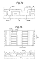
- Figure 7a shows a cross-sectional view of filled and under filled tungsten markers from the prior art, before W-CMP.
- tungsten is deposited by a CVD process in blanket mode.
- Figure 7a illustrates that the width of the trench governs whether the conformally grown tungsten layer fills the trench in a 'filled' or 'underfilled' mode.
- the bottom of the trench may be covered by a barrier layer.
- a CMP process is carried out to planarise the structure.
- a metal (W) structure with a surface substantially on level with the silicon dioxide surface is formed.
- the phase depth of the 'filled' structure is substantially zero.
- the 'underfilled' metal structure comprises portions (i.e., the side-walls) which are substantially on level with the silicon dioxide surface, and a central portion which surface is well below the silicon dioxide surface level.
- the central W portion has a given phase depth relative to the silicon dioxide surface level.
- the width of the trench determines whether a tungsten line will either be filled or underfilled.
- the phase depth will comprise two discrete levels as a function of the trench width.
- the CMP process can not be controlled very accurately.
- the depth of the central portion of the metal line may be such that the phase depth is substantially zero: no control over the phase depth is obtained.
- Figure 7b shows a planar view (TOP) and a cross-sectional view (SIDE) of a tungsten marker structure in silicon dioxide according to a sixth embodiment of the present invention.
- the optical marker structure comprises tungsten sub-segments in the silicon dioxide lines.
- a plurality of sub-trenches are formed in the silicon dioxide lines, with the length direction of sub-trenches extending in a direction parallel to the periodicity P of the marker structure. Since the plurality of sub-trenches are periodically arranged in a direction which will be a so-called non-scanning direction during alignment procedures, the optical response on the periodic arrangement of the sub-trenches in that direction Psub is not detected by an alignment- or overlay-sensor system.
- the possible diffraction signal generated by (the periodicity of) the sub-trenches is directed in a direction perpendicular to the direction of the diffraction signal of the actual marker structure (i.e., the repetition of tungsten trenches and silicon dioxide lines), so this possible signal will be well outside of the detection region.
- the trenches and sub-trenches are filled with tungsten by a tungsten CVD process.
- a CMP process is carried out to planarise the structure. Due to the presence of tungsten in the sub-trenches, the CMP process is in better control: .
- the area of the marker structure comprising filled structures with its specific resistance to CMP is relatively enlarged, which allows polishing of the filled trenches to a given height with greater accuracy.
- the phase depth may be controlled.
- the height of the top level of the filled tungsten structure relative to the lower level of tungsten in the underfilled region may be adapted to obtain a desired phase depth.
- the phase depth may be adapted by changing the spacing between the sub-trenches (and their number) in the silicon dioxide lines to change the relative area of filled W structures.
- the width of the sub-trenches is double of the thickness of the conformal tungsten layer (which thus results in a completely filled sub-trench having a zero phase depth).
- optical markers on IC processing may lead to undesirable side effects due to the fact that the optical markers are inherently larger than feature sizes in integrated circuits.
- the minimum feature size of markers is in the order of 1 ⁇ m.
- the typical minimal feature size is about 100 nm (depending on the device generation). Since the marker usually consists of the same material as (part of) the devices, the presence of an additional marker area of a substantial size in the vicinity of a device may have an influence on the local processing rate for that device in a given processing step.
- a chemical reaction in a reactive ion etching process or a chemical deposition process may be influenced by the presence of a large marker area due to some kinetic constraint, or due to a local deviation of the wafer temperature, etc.
- a chemical mechanical polishing process may be influenced by the presence of a large marker area due to some mechanical constraint (i.e., a higher or lower resistance to CMP) caused by the marker area.
- a size difference between marker and device feature may thus lead to modification of a processing step for devices located closely to a marker. Due to the modification of the processing a variation of device characteristics may occur across a die and/or a wafer.
- the optical marker structure from the prior art requires to be segmented in such a way that critical device features are better mimicked while the diffraction pattern generated by the modified marker structure remains substantially the same as for an unmodified marker from the prior art.
- the alignment system is arranged in such a way that polarisation effects results in usable signal strength of measured signals.
- Figure 8 shows a planar view of a marker structure according to a seventh embodiment of the present invention.
- the first structural elements are sub-segmented in a plurality of primary lines L1 extending in a first direction D1, each primary line having a width comparable to critical feature sizes of a device.
- each primary line having a width comparable to critical feature sizes of a device.
- interposed lines of a different material. The width of the primary and interposed lines is such that dense device structures with critical feature sizes are mimicked.
- the second structural elements in between the first structural elements are sub-segmented in a plurality of secondary lines L2 extending in a second direction D2, with interposed lines of a different material in between.
- the secondary lines and interposed lines have widths comparable to dense device structures with the critical feature sizes for devices.
- the second direction D2 is perpendicular to the first direction D1.
- the material of the primary lines and the secondary lines is typically the same, e.g., a metal, while the material in between the primary lines and in between the secondary lines may be a dielectric or semiconductor.
- the width of the primary line may or may not be equal to the width of a secondary line.
- the alignment system uses a first laser beam with a first linear polarisation E1 and a second laser beam with a second linear polarisation E2.
- the wavelength of the first laser beam differs from the wavelength of the second laser beam.
- the first laser beam consists of red light
- the second laser beam of green light.
- the first linear polarisation direction E1 is perpendicular to the second linear polarisation direction E2. Further, the first linear polarisation E1 is arranged in such a way that the line segments L1 in the marker lines allow a further transmission of the first polarised light beam in order to form a diffraction pattern of the marker structure. Similarly, the second linear polarisation E2 is arranged in such a way that the line segments L2 in the intermediate marker elements allow a further transmission of the second polarised light beam to form a diffraction pattern of the marker structure.
- Figure 9 shows an application of a stack of markers in accordance with the seventh embodiment of the present invention.
- a further advantage of the structure of the seventh embodiment is the fact that at least two of such markers can be stacked on top of each other, without causing any interference between them.
- the needed estate for the marker structures in the scribelane can be significantly reduced.
- a second marker OM2 is translated over half the periodicity P with respect to the first marker OM1, with the width of "lines” being equal to the width of "trenches”. Due to the segmentation of the "trenches” and “lines” perpendicular to each other, the polarisation effect prohibits cross-talk between the upper and lower marker structure.
- the alignment system only detects the upper marker structure.
Landscapes
- Physics & Mathematics (AREA)
- General Physics & Mathematics (AREA)
- Engineering & Computer Science (AREA)
- Signal Processing (AREA)
- Multimedia (AREA)
- Exposure And Positioning Against Photoresist Photosensitive Materials (AREA)
Priority Applications (45)
| Application Number | Priority Date | Filing Date | Title |
|---|---|---|---|
| EP03076422A EP1477860A1 (de) | 2003-05-12 | 2003-05-12 | Zur Herstellung eines mikroelektronischen Elements geeignete Struktur einer lithographischen Marke |
| CNB03164841XA CN100337089C (zh) | 2002-09-20 | 2003-09-19 | 器件检验 |
| TW092125961A TWI227814B (en) | 2002-09-20 | 2003-09-19 | Alignment system and methods for lithographic systems using at least two wavelengths |
| EP20030077976 EP1400860B1 (de) | 2002-09-20 | 2003-09-19 | Lithographische Markierungsstruktur, lithographischer Projektionsapparat mit einer solchen Markierungsstruktur und Verfahren zur Ausrichtung eines Substrates unter Verwendung einer solchen Markierungsstruktur |
| SG200305608A SG120949A1 (en) | 2002-09-20 | 2003-09-19 | Alignment system and methods for lithographic systems using at least two wavelengths |
| CN031648584A CN1495540B (zh) | 2002-09-20 | 2003-09-19 | 利用至少两个波长的光刻系统的对准系统和方法 |
| JP2003366659A JP4362347B2 (ja) | 2002-09-20 | 2003-09-19 | リソグラフィ用マーカ構造、このようなリソグラフィ用マーカ構造を備えるリソグラフィ投影機器およびこのようなリソグラフィ用マーカ構造を使用して基板を位置合わせする方法 |
| SG200305609A SG125923A1 (en) | 2002-09-20 | 2003-09-19 | Lithographic marker structure, lithographic projection apparatus comprising such a lithographic marker structure and method for substrate alignment using such a lithographic marker structure |
| EP03077974A EP1400854A3 (de) | 2002-09-20 | 2003-09-19 | Systeme und Verfahren zum Ausrichten für Lithographische Systeme |
| JP2003366657A JP2004282017A (ja) | 2002-09-20 | 2003-09-19 | リソグラフィ装置の位置決めシステムおよび方法 |
| JP2003366658A JP4222927B2 (ja) | 2002-09-20 | 2003-09-19 | 少なくとも2波長を使用するリソグラフィ装置用アライメント・システム |
| CN031648592A CN1506768B (zh) | 2002-09-20 | 2003-09-19 | 用于光刻系统的对准系统和方法 |
| EP10161132A EP2204697A3 (de) | 2002-09-20 | 2003-09-19 | Markerstruktur, lithographische Projektionsvorrichtung, Verfahren zur Substratausrichtung mittels solch einer Struktur und Substrat mit solch einer Markerstruktur |
| EP03077973A EP1400859A3 (de) | 2002-09-20 | 2003-09-19 | System und Verfahren zur Ausrichtung lithographischer Systeme unter Verwendung mindestens zweier Wellenlängen |
| TW092125932A TWI229243B (en) | 2002-09-20 | 2003-09-19 | Lithographic marker structure, lithographic projection apparatus comprising such a lithographic marker structure and method for substrate alignment using such a lithographic marker structure |
| JP2003366656A JP4222926B2 (ja) | 2002-09-20 | 2003-09-19 | デバイス検査 |
| KR1020030065299A KR100632889B1 (ko) | 2002-09-20 | 2003-09-19 | 2개이상의 파장을 사용하는 리소그래피시스템용정렬시스템 및 정렬방법 |
| SG200305606-6A SG152898A1 (en) | 2002-09-20 | 2003-09-19 | Alignment systems and methods for lithographic systems |
| KR1020030065268A KR100552455B1 (ko) | 2002-09-20 | 2003-09-19 | 리소그래피시스템용 정렬시스템 및 정렬방법 |
| KR1020030065281A KR100543536B1 (ko) | 2002-09-20 | 2003-09-19 | 리소그래피 마커구조체, 상기 리소그래피 마커구조체를포함하는 리소그래피 투영장치 및 상기 리소그래피마커구조체를 사용하여 기판을 정렬하는 방법 |
| CNB031648401A CN100476599C (zh) | 2002-09-20 | 2003-09-19 | 光刻标记结构、包含该光刻标记结构的光刻投射装置和利用该光刻标记结构进行基片对准的方法 |
| SG200305607A SG125922A1 (en) | 2002-09-20 | 2003-09-19 | Device inspection |
| KR1020030065314A KR100597041B1 (ko) | 2002-09-20 | 2003-09-19 | 디바이스 검사방법 및 장치 |
| TW092125977A TWI277842B (en) | 2002-09-20 | 2003-09-19 | Alignment systems and methods for lithographic systems |
| EP03077975A EP1400855A3 (de) | 2002-09-20 | 2003-09-19 | Inspektion eines Artikels |
| TW092125934A TWI251722B (en) | 2002-09-20 | 2003-09-19 | Device inspection |
| US10/665,404 US7332732B2 (en) | 2002-09-20 | 2003-09-22 | Alignment systems and methods for lithographic systems |
| US10/665,360 US7330261B2 (en) | 2002-09-20 | 2003-09-22 | Marker structure for optical alignment of a substrate, a substrate including such a marker structure, an alignment method for aligning to such a marker structure, and a lithographic projection apparatus |
| US10/665,364 US6844918B2 (en) | 2002-09-20 | 2003-09-22 | Alignment system and methods for lithographic systems using at least two wavelengths |
| US10/665,720 US7112813B2 (en) | 2002-09-20 | 2003-09-22 | Device inspection method and apparatus using an asymmetric marker |
| KR10-2005-0090920A KR100536632B1 (ko) | 2002-09-20 | 2005-09-29 | 리소그래피 장치용 메트롤로지 시스템 |
| US11/294,559 US7297971B2 (en) | 2002-09-20 | 2005-12-06 | Alignment systems and methods for lithographic systems |
| US11/294,473 US20060081790A1 (en) | 2002-09-20 | 2005-12-06 | Alignment systems and methods for lithographic systems |
| US11/294,475 US20060081791A1 (en) | 2002-09-20 | 2005-12-06 | Alignment systems and methods for lithographic systems |
| US11/294,367 US7880880B2 (en) | 2002-09-20 | 2005-12-06 | Alignment systems and methods for lithographic systems |
| US11/294,476 US7329888B2 (en) | 2002-09-20 | 2005-12-06 | Alignment systems and methods for lithographic systems |
| US11/643,772 US7439531B2 (en) | 2002-09-20 | 2006-12-22 | Alignment systems and methods for lithographic systems |
| JP2007009156A JP4166810B2 (ja) | 2002-09-20 | 2007-01-18 | リソグラフィ用マーカ構造、このようなリソグラフィ用マーカ構造を備えるリソグラフィ投影機器およびこのようなリソグラフィ用マーカ構造を使用して基板を位置合わせする方法 |
| JP2007236876A JP2007335906A (ja) | 2002-09-20 | 2007-09-12 | 少なくとも2波長を使用するリソグラフィ装置用アライメント・システム |
| JP2007267899A JP2008034878A (ja) | 2002-09-20 | 2007-10-15 | リソグラフィ装置の位置決めシステムおよび方法 |
| US12/003,377 US7619738B2 (en) | 2002-09-20 | 2007-12-21 | Marker structure for optical alignment of a substrate, a substrate including such a marker structure, an alignment method for aligning to such a marker structure, and a lithographic projection apparatus |
| JP2008119913A JP4422774B2 (ja) | 2002-09-20 | 2008-05-01 | マーカ構造、位置合わせ方法、超小型電子デバイス用の基板、およびリソグラフィ投影機器 |
| JP2008307147A JP4972628B2 (ja) | 2002-09-20 | 2008-12-02 | リソグラフィ装置の位置決めシステム |
| US12/977,541 US8139217B2 (en) | 2002-09-20 | 2010-12-23 | Alignment systems and methods for lithographic systems |
| JP2012022300A JP5508448B2 (ja) | 2002-09-20 | 2012-02-03 | アライメントマーク |
Applications Claiming Priority (1)
| Application Number | Priority Date | Filing Date | Title |
|---|---|---|---|
| EP03076422A EP1477860A1 (de) | 2003-05-12 | 2003-05-12 | Zur Herstellung eines mikroelektronischen Elements geeignete Struktur einer lithographischen Marke |
Publications (1)
| Publication Number | Publication Date |
|---|---|
| EP1477860A1 true EP1477860A1 (de) | 2004-11-17 |
Family
ID=33016937
Family Applications (1)
| Application Number | Title | Priority Date | Filing Date |
|---|---|---|---|
| EP03076422A Withdrawn EP1477860A1 (de) | 2002-09-20 | 2003-05-12 | Zur Herstellung eines mikroelektronischen Elements geeignete Struktur einer lithographischen Marke |
Country Status (1)
| Country | Link |
|---|---|
| EP (1) | EP1477860A1 (de) |
Cited By (5)
| Publication number | Priority date | Publication date | Assignee | Title |
|---|---|---|---|---|
| WO2009072881A1 (en) * | 2007-12-05 | 2009-06-11 | Asml Netherlands B.V. | Marker structure and method of forming the same |
| WO2010025793A1 (en) * | 2008-09-08 | 2010-03-11 | Asml Netherlands B.V. | A substrate, a method of measuring a property, an inspection apparatus and a lithographic apparatus |
| EP3203322A1 (de) * | 2016-02-03 | 2017-08-09 | Semiconductor Manufacturing International Corporation (Shanghai) | Markierungsstruktur und herstellungsverfahren dafür |
| US10322467B2 (en) | 2015-01-28 | 2019-06-18 | Tokyo Seimitsu Co., Ltd. | Position detecting device and laser processing device |
| CN109901359A (zh) * | 2017-12-11 | 2019-06-18 | 长鑫存储技术有限公司 | 用于掩膜的对准图形、掩膜及晶圆 |
Citations (2)
| Publication number | Priority date | Publication date | Assignee | Title |
|---|---|---|---|---|
| US6420791B1 (en) * | 1999-11-23 | 2002-07-16 | United Microelectronics Corp. | Alignment mark design |
| US20020158193A1 (en) * | 2001-02-12 | 2002-10-31 | Abdurrahman Sezginer | Overlay alignment metrology using diffraction gratings |
-
2003
- 2003-05-12 EP EP03076422A patent/EP1477860A1/de not_active Withdrawn
Patent Citations (2)
| Publication number | Priority date | Publication date | Assignee | Title |
|---|---|---|---|---|
| US6420791B1 (en) * | 1999-11-23 | 2002-07-16 | United Microelectronics Corp. | Alignment mark design |
| US20020158193A1 (en) * | 2001-02-12 | 2002-10-31 | Abdurrahman Sezginer | Overlay alignment metrology using diffraction gratings |
Cited By (11)
| Publication number | Priority date | Publication date | Assignee | Title |
|---|---|---|---|---|
| WO2009072881A1 (en) * | 2007-12-05 | 2009-06-11 | Asml Netherlands B.V. | Marker structure and method of forming the same |
| US8319967B2 (en) * | 2007-12-05 | 2012-11-27 | Asml Netherlands B.V. | Marker structure and method of forming the same |
| WO2010025793A1 (en) * | 2008-09-08 | 2010-03-11 | Asml Netherlands B.V. | A substrate, a method of measuring a property, an inspection apparatus and a lithographic apparatus |
| US9229338B2 (en) | 2008-09-08 | 2016-01-05 | Asml Netherlands B.V. | Substrate, a method of measuring a property, an inspection apparatus and a lithographic apparatus |
| US9255892B2 (en) | 2008-09-08 | 2016-02-09 | Asml Netherlands B.V. | Substrate, a method of measuring a property, an inspection apparatus and a lithographic apparatus |
| US10322467B2 (en) | 2015-01-28 | 2019-06-18 | Tokyo Seimitsu Co., Ltd. | Position detecting device and laser processing device |
| EP3203322A1 (de) * | 2016-02-03 | 2017-08-09 | Semiconductor Manufacturing International Corporation (Shanghai) | Markierungsstruktur und herstellungsverfahren dafür |
| CN107037699A (zh) * | 2016-02-03 | 2017-08-11 | 中芯国际集成电路制造(上海)有限公司 | 标记结构的形成方法 |
| US9773739B2 (en) | 2016-02-03 | 2017-09-26 | Semiconductor Manufacturing International (Shanghai) Corporation | Mark structure and fabrication method thereof |
| CN107037699B (zh) * | 2016-02-03 | 2019-01-29 | 中芯国际集成电路制造(上海)有限公司 | 标记结构的形成方法 |
| CN109901359A (zh) * | 2017-12-11 | 2019-06-18 | 长鑫存储技术有限公司 | 用于掩膜的对准图形、掩膜及晶圆 |
Similar Documents
| Publication | Publication Date | Title |
|---|---|---|
| US7619738B2 (en) | Marker structure for optical alignment of a substrate, a substrate including such a marker structure, an alignment method for aligning to such a marker structure, and a lithographic projection apparatus | |
| US7466413B2 (en) | Marker structure, mask pattern, alignment method and lithographic method and apparatus | |
| US7759029B2 (en) | Substrate provided with an alignment mark in a substantially transmissive process layer, mask for exposing said mark, device manufacturing method, and device manufactured thereby | |
| EP1548507B1 (de) | Substratverarbeitungsverfahren | |
| KR20070092155A (ko) | 리소그래피 정렬 개선 방법 및 시스템 | |
| WO2002065545A2 (en) | Overlay alignment metrology using diffraction gratings | |
| US8609441B2 (en) | Substrate comprising a mark | |
| EP1400860A2 (de) | Lithographische Markierungsstruktur, lithographischer Projektionsapparat mit einer solchen Markierungsstruktur und Verfahren zur Ausrichtung eines Substrates unter Verwendung einer solchen Markierungsstruktur | |
| KR100550031B1 (ko) | 리소그래피장치, 정렬방법 및 디바이스 제조방법 | |
| US8722179B2 (en) | Substrate comprising a mark | |
| US8319967B2 (en) | Marker structure and method of forming the same | |
| EP1260870A1 (de) | Ausrichtmarke | |
| EP1260869A1 (de) | Substrat mit Ausrichtungsmarke in einer wesentlich transparenten Prozessschicht | |
| EP1338924B1 (de) | Verfahren zur Ausrichtung und Verfahren zur Herstellung eines Artikels | |
| EP1469355B1 (de) | Verfahren zur Herstellung einer Vorrichtung |
Legal Events
| Date | Code | Title | Description |
|---|---|---|---|
| PUAI | Public reference made under article 153(3) epc to a published international application that has entered the european phase |
Free format text: ORIGINAL CODE: 0009012 |
|
| AK | Designated contracting states |
Kind code of ref document: A1 Designated state(s): AT BE BG CH CY CZ DE DK EE ES FI FR GB GR HU IE IT LI LU MC NL PT RO SE SI SK TR |
|
| AX | Request for extension of the european patent |
Extension state: AL LT LV MK |
|
| AKX | Designation fees paid | ||
| REG | Reference to a national code |
Ref country code: DE Ref legal event code: 8566 |
|
| STAA | Information on the status of an ep patent application or granted ep patent |
Free format text: STATUS: THE APPLICATION IS DEEMED TO BE WITHDRAWN |
|
| 18D | Application deemed to be withdrawn |
Effective date: 20050518 |