EP1477998A2 - Anode für Elektrolytkondensatoren, Elektrolytkondensator und Verfahren zur Herstellung der Anode - Google Patents
Anode für Elektrolytkondensatoren, Elektrolytkondensator und Verfahren zur Herstellung der Anode Download PDFInfo
- Publication number
- EP1477998A2 EP1477998A2 EP04017526A EP04017526A EP1477998A2 EP 1477998 A2 EP1477998 A2 EP 1477998A2 EP 04017526 A EP04017526 A EP 04017526A EP 04017526 A EP04017526 A EP 04017526A EP 1477998 A2 EP1477998 A2 EP 1477998A2
- Authority
- EP
- European Patent Office
- Prior art keywords
- anode
- conductor
- anode conductor
- tantalum
- paste
- Prior art date
- Legal status (The legal status is an assumption and is not a legal conclusion. Google has not performed a legal analysis and makes no representation as to the accuracy of the status listed.)
- Withdrawn
Links
- 239000003990 capacitor Substances 0.000 title claims abstract description 61
- 238000000034 method Methods 0.000 title claims abstract description 32
- 238000004519 manufacturing process Methods 0.000 claims abstract description 19
- 239000000463 material Substances 0.000 claims abstract description 14
- GUVRBAGPIYLISA-UHFFFAOYSA-N tantalum atom Chemical compound [Ta] GUVRBAGPIYLISA-UHFFFAOYSA-N 0.000 claims description 69
- 239000004020 conductor Substances 0.000 claims description 56
- 229910052715 tantalum Inorganic materials 0.000 claims description 47
- 229910052751 metal Inorganic materials 0.000 claims description 26
- 239000002184 metal Substances 0.000 claims description 26
- 239000000843 powder Substances 0.000 claims description 24
- 238000005245 sintering Methods 0.000 claims description 8
- 238000003825 pressing Methods 0.000 claims description 7
- 239000011230 binding agent Substances 0.000 claims description 6
- 238000007639 printing Methods 0.000 claims description 6
- 239000000654 additive Substances 0.000 claims description 5
- 230000000996 additive effect Effects 0.000 claims description 5
- 229910052758 niobium Inorganic materials 0.000 claims description 4
- 239000010955 niobium Substances 0.000 claims description 4
- GUCVJGMIXFAOAE-UHFFFAOYSA-N niobium atom Chemical compound [Nb] GUCVJGMIXFAOAE-UHFFFAOYSA-N 0.000 claims description 4
- 125000006850 spacer group Chemical group 0.000 claims description 4
- 238000007650 screen-printing Methods 0.000 claims description 3
- DSSYKIVIOFKYAU-XCBNKYQSSA-N (R)-camphor Chemical compound C1C[C@@]2(C)C(=O)C[C@@H]1C2(C)C DSSYKIVIOFKYAU-XCBNKYQSSA-N 0.000 claims description 2
- 241000723346 Cinnamomum camphora Species 0.000 claims description 2
- 229960000846 camphor Drugs 0.000 claims description 2
- 229930008380 camphor Natural products 0.000 claims description 2
- 230000001050 lubricating effect Effects 0.000 claims description 2
- 239000011148 porous material Substances 0.000 claims description 2
- 238000005538 encapsulation Methods 0.000 claims 2
- 229910001092 metal group alloy Inorganic materials 0.000 claims 2
- 238000007765 extrusion coating Methods 0.000 claims 1
- 238000007493 shaping process Methods 0.000 claims 1
- 230000008569 process Effects 0.000 abstract description 7
- 239000007787 solid Substances 0.000 abstract description 3
- 238000001035 drying Methods 0.000 description 6
- 238000000465 moulding Methods 0.000 description 4
- 230000015572 biosynthetic process Effects 0.000 description 3
- 230000004048 modification Effects 0.000 description 3
- 238000012986 modification Methods 0.000 description 3
- 239000002245 particle Substances 0.000 description 3
- 230000007704 transition Effects 0.000 description 3
- 239000000853 adhesive Substances 0.000 description 2
- 230000001070 adhesive effect Effects 0.000 description 2
- 230000008901 benefit Effects 0.000 description 2
- 238000013461 design Methods 0.000 description 2
- 239000006185 dispersion Substances 0.000 description 2
- 230000000694 effects Effects 0.000 description 2
- 150000002739 metals Chemical class 0.000 description 2
- 238000013021 overheating Methods 0.000 description 2
- BPUBBGLMJRNUCC-UHFFFAOYSA-N oxygen(2-);tantalum(5+) Chemical compound [O-2].[O-2].[O-2].[O-2].[O-2].[Ta+5].[Ta+5] BPUBBGLMJRNUCC-UHFFFAOYSA-N 0.000 description 2
- PBCFLUZVCVVTBY-UHFFFAOYSA-N tantalum pentoxide Inorganic materials O=[Ta](=O)O[Ta](=O)=O PBCFLUZVCVVTBY-UHFFFAOYSA-N 0.000 description 2
- 229910045601 alloy Inorganic materials 0.000 description 1
- 239000000956 alloy Substances 0.000 description 1
- 238000010276 construction Methods 0.000 description 1
- 238000005520 cutting process Methods 0.000 description 1
- 238000001125 extrusion Methods 0.000 description 1
- -1 for example niobium Chemical class 0.000 description 1
- 230000006870 function Effects 0.000 description 1
- 230000006872 improvement Effects 0.000 description 1
- 238000012805 post-processing Methods 0.000 description 1
- 238000012545 processing Methods 0.000 description 1
- 230000009993 protective function Effects 0.000 description 1
- 238000007711 solidification Methods 0.000 description 1
- 230000008023 solidification Effects 0.000 description 1
- 150000003481 tantalum Chemical class 0.000 description 1
Images


Classifications
-
- H—ELECTRICITY
- H01—ELECTRIC ELEMENTS
- H01G—CAPACITORS; CAPACITORS, RECTIFIERS, DETECTORS, SWITCHING DEVICES, LIGHT-SENSITIVE OR TEMPERATURE-SENSITIVE DEVICES OF THE ELECTROLYTIC TYPE
- H01G9/00—Electrolytic capacitors, rectifiers, detectors, switching devices, light-sensitive or temperature-sensitive devices; Processes of their manufacture
- H01G9/004—Details
- H01G9/008—Terminals
- H01G9/012—Terminals specially adapted for solid capacitors
-
- H—ELECTRICITY
- H01—ELECTRIC ELEMENTS
- H01G—CAPACITORS; CAPACITORS, RECTIFIERS, DETECTORS, SWITCHING DEVICES, LIGHT-SENSITIVE OR TEMPERATURE-SENSITIVE DEVICES OF THE ELECTROLYTIC TYPE
- H01G9/00—Electrolytic capacitors, rectifiers, detectors, switching devices, light-sensitive or temperature-sensitive devices; Processes of their manufacture
- H01G9/004—Details
- H01G9/04—Electrodes or formation of dielectric layers thereon
- H01G9/042—Electrodes or formation of dielectric layers thereon characterised by the material
-
- H—ELECTRICITY
- H01—ELECTRIC ELEMENTS
- H01G—CAPACITORS; CAPACITORS, RECTIFIERS, DETECTORS, SWITCHING DEVICES, LIGHT-SENSITIVE OR TEMPERATURE-SENSITIVE DEVICES OF THE ELECTROLYTIC TYPE
- H01G9/00—Electrolytic capacitors, rectifiers, detectors, switching devices, light-sensitive or temperature-sensitive devices; Processes of their manufacture
- H01G9/004—Details
- H01G9/04—Electrodes or formation of dielectric layers thereon
- H01G9/048—Electrodes or formation of dielectric layers thereon characterised by their structure
- H01G9/052—Sintered electrodes
-
- H—ELECTRICITY
- H01—ELECTRIC ELEMENTS
- H01G—CAPACITORS; CAPACITORS, RECTIFIERS, DETECTORS, SWITCHING DEVICES, LIGHT-SENSITIVE OR TEMPERATURE-SENSITIVE DEVICES OF THE ELECTROLYTIC TYPE
- H01G9/00—Electrolytic capacitors, rectifiers, detectors, switching devices, light-sensitive or temperature-sensitive devices; Processes of their manufacture
- H01G9/15—Solid electrolytic capacitors
Definitions
- the present invention relates to an anode for electrolytic capacitors with an anode body and an anode conductor.
- the invention further relates to an electrolytic capacitor with the anode, a dielectric surrounding the anode, a layer cathode provided on the dielectric, a first connection tab formed from the anode conductor and a second connection tab connected to the layer cathode.
- the present invention further relates to methods for the manufacture of the anode.
- the capacitor is preferably a Chip capacitor.
- the present invention is without further also on other capacitors, such as housingless capacitors, applicable.
- a caseless capacitor has a low overall height and is used, for example, in a hybrid circuit integrated. In the following, however, of it be assumed that the capacitor of the invention is a chip capacitor.
- Chip capacitors especially tantalum chip capacitors are characterized by a high volume-specific capacitance-voltage product, also called "CV product”. This means, for these capacitors, the value is based on volume Product of capacitance and attachable to the capacitor Tension particularly great.
- CV product volume-specific capacitance-voltage product
- FIG. 24 shows the structure of a conventional tantalum chip capacitor in a schematic section, while in FIG. 25 the anode body of this chip capacitor in a side view and in Fig. 26 the anode body is shown in plan view is.
- This conventional chip capacitor consists of the anode body 1, a dielectric 2 and a layer cathode 3, which form an actual capacitor element.
- a housing 4 is provided, the important protective functions takes over for the capacitor element.
- the dielectric 2 and the layer cathode 3 carries a tantalum wire 5, the inside of the housing 4 with a first metal ash 6 connected is.
- the layer cathode is by means of a conductive adhesive 8 3 connected to a second metal ash 7, which like the metal ash 6 is led out of the housing 4.
- Such chip capacitors come in different sizes the housing 4 with mostly standardized base dimensions and Heights made. Consequently, to achieve a higher one CV product the volume fraction of the capacitor element or of the anode body 1 contained therein.
- the tantalum wire 5 in the anode body 1 (cf. in particular also FIGS. 25 and 26) as anode-side
- the housing can hardly be used as a surge arrester be increased.
- the free end of the tantalum wire 5 is namely welded to the metal ash 6, which in the finished Chip capacitor electrical connection to an electronic Circuit on one circuit board together with the other Should take over metal ash.
- the distance between the capacitor element is especially on the plus side and the housing wall is particularly large.
- the through the Tantalum wire 5 formed distance between the plus-side metal ash 6 and the capacitor element or the anode body 1 can hardly be further reduced due to production. With in other words, in the known chip capacitor Housing volume is underused.
- a tantalum chip capacitor is known from the publication DD-PS 215 420 known in which an anode arrester in a two-part anode body prefabricated by extrusion is embedded. Then the anode body with the Sintered anode arrester.
- the use of two pre-pressed Part anode bodies has the disadvantage that due to manufacturing Tolerances not an exact form fit of the Anode body can be achieved with the anode arrester. As a result, the electrical contact between deteriorates Anode body and anode conductor.
- the aim of the present invention is therefore to provide an anode which has a large contact area between the anode conductor and the anode body, the anode body of which has a predefined shape and a good electrical one There is contact between the anode body and the anode conductor.
- the invention provides an anode for an electrolytic capacitor with a fixed anode body Form and with a flat anode conductor, in which the anode body from a continuously deformable material, which can be solidified, molded onto the anode conductor is.
- the invention provides a capacitor in which the Anode body is surrounded by a dielectric, on which a layer cathode is provided in the dielectric, in which a further end section of the anode conductor to a first Connection tab is formed and in which the layer cathode with a second connecting strap is connected.
- the anode according to the invention has the advantage that by molding of the entire anode body in the form of a continuous deformable material on the anode conductor a homogeneous Anode body with a good form fit to the anode conductor as well as with good electrical contact to the anode arrester can be designed.
- the anode according to the invention has the advantage that the shape of the anode body using a continuous deformable material with any shape Help appropriate forms before or after solidification of the anode body can be removed.
- the material, from which the anode body is formed for example a paste containing metal powder, one from the paste manufactured green film or a suitable metal powder be yourself.
- anode arrester which in the Anode body sintered from, for example, sintered tantalum powder is compared to a sintered tantalum wire with the same cross-sectional area, a larger contact area reached between anode conductor and anode body.
- the number of powder particles covering the surface of the anode conductor touch is increased, and thus the average Length of the tantalum particles sintered together existing current paths between the dielectric and the anode conductor is reduced. As a result, you can reduced resistance values and increased capacity high frequencies can be achieved.
- Essential to the capacitor or anode according to the invention is in particular the realization of a solid and large area Connection between the anode body from a capacitance-forming, open-pore sintered body and an anode conductor with a large surface.
- tantalum or another suitable metal such as Niobium or a material used to form a Permitted layer with a high dielectric constant.
- An anode is also advantageous, in which the anode body an end portion of the anode conductor completely encloses. This allows optimal use of the surface of the anode conductor for contacting the anode body be achieved. Furthermore, this is a high mechanical Anode stability guaranteed.
- the invention provides a method for producing the anode according to the invention, a continuously deformable Material that can be solidified under simultaneous external shape to a flat anode conductor molded and then to form an anode body is solidified.
- a continuously deformable Material that can be solidified under simultaneous external shape to a flat anode conductor molded and then to form an anode body is solidified.
- a method is particularly advantageous in which a paste, which contains a binder system and a powder on the anode conductor applied and then dried and sintered becomes.
- the paste can be done using different methods can be designed into an anode using the anode arrester. It can for example one from the publication DE 199 27 909 A1 known paste consisting of a discrete phase with a metal powder and a continuous phase with organic Connections are used.
- the invention also provides a method for producing the anode according to the invention, wherein a flat anode conductor is pressed with a powder from which the anode conductor protrudes on one side. Then the compact sintered.
- the method according to the invention can advantageously do so be carried out that an anode conductor in the form of a strip-shaped sheet in a located in a press die Fill is inserted from the powder and then the pressing process takes place.
- the preferred material for the anode conductor is tantalum is very expensive, so that used for the process Strips should be as thin as possible. On the other hand, it has to tantalum sheet used sufficient mechanical stability have so that it is inserted into the powder bed and later bent into a mechanically stable tab can. Under these boundary conditions, stripe-shaped Anode arrester with a width between 0.3 and 5 mm and one Thickness between 50 and 150 ⁇ m has been found to be suitable. This anode arrester have a width / thickness ratio between 2 and 100 on.
- Cross presses are done, d. H. by pressing across the direction, in which the strip-shaped anode arrester extends.
- the further production steps correspond to the conventional ones Tantalum chip capacitor manufacturing. So in the formation mentioned procedure on the inner and outer surface of the sintered anode body, the dielectric made of tantalum pentoxide educated. After the application of the cathode layers follows the production of the cathode connection and housing.
- the anode tab for the plus side electrical connection made of tantalum in the embodiment according to the invention for Purposes of solderability or bondability are treated what also applies to the other exemplary embodiments.
- Tantalum chip capacitor is the tantalum powder with one Additive added that due to its lubricating effect Pressing process made easier and protects the pressing tool. Also the flowability of the powder and the mechanical Stability of the compact due to the binding effect of the additive improved.
- a common additive is camphor. It should residue-free if possible before sintering the compact be removed.
- tantalum instead of tantalum, other suitable metals, such as for example niobium, or alloys of suitable metals or other materials that have the ability to Have formation of a dielectric can be used.
- suitable metals such as for example niobium, or alloys of suitable metals or other materials that have the ability to Have formation of a dielectric can be used.
- the anode body 1 shows a chip capacitor according to the invention with a actual capacitor element from an anode body 1, a dielectric 2, a layer cathode 3 and a flat one Anode conductor 9, which extends into the anode body 1.
- the anode body 1 consists of a porous metal sintered body, the, as will be explained in more detail below is made from a paste containing metal powder, which is dried and is sintered, is built up and thereby a solid and large-area connection with the anode conductor 9.
- the anode conductor 9 is preferably made of tantalum, the advantageously as a metal for the Metal powder of the paste is used.
- the layer cathode 3 is like the conventional chip capacitor 24 via a conductive adhesive 8 with the metal ash 7 connected.
- the anode conductor 9 fulfills the functions of the tantalum wire 5 and the metal ash 6 of the conventional chip capacitor 24: For this purpose, it is bent into a contact tab or formed (see. In particular Fig. 2 and 3), whereby on the plus side, the distance between the capacitor element and the edge of the housing 4 can be reduced.
- the volume the housing 4 of the component is thus better utilized, to advantageously achieve a higher CV product. Even if the volume of the anode body 1 remains the same a smaller size can be chosen for the housing 4. at same size of the housing 4 can by the invention Capacitor element or the anode body 1 is made larger 24 to 26 as in the prior art.
- the chip capacitor according to the invention with the flat anode conductor 9 in the anode body 1 allows the production extremely flat capacitor elements, like this schematically 4 to 6 can be seen.
- 5 shows how 2 is a side view of the anode body 1 with the Anode arrester 9, while in Fig. 6, similar to that in the Fig. 3, a plan view of the anode body 1 with the anode conductor 9 is shown.
- the anode conductor 9 is shown in its entire extent, although in part it is through the anode body 1 is covered.
- a paste is used to produce an anode body a binder system and a tantalum powder on a tantalum foil or a tantalum sheet 10 with a thickness of 50 to 150 ⁇ m below Printed using a stencil 11.
- Fig. 7 shows one Top view of this template 11, while in Fig. 8 a side view of the tantalum sheet 10 together with the template 11 9 and the template 11 is filled with tantalum paste 12 in FIG is.
- Fig. 10 shows a side view of such an anode body with a tantalum sheet 10, while in Fig. 13 a Top view of this is shown.
- the subsequent process steps correspond to the conventional tantalum chip capacitor production. So in one Formation procedure called on the inner and outer Surface of the sintered anode body 1, the dielectric 2 formed from tantalum pentoxide. After applying the layer cathode 3 follows the production of the cathode connection or metal ash 7 and housing 4.
- the plus-side electrical Connection serving anode tab from the anode arrester 9 Tantalum can be used for the purpose of improving the solderability or bondability still to be treated.
- FIG. 7 to 13 is a modification of the exemplary embodiment it is possible to tantalum sheet 10 on both sides with the tantalum paste 12 to print what can be done in one operation.
- the Printing in two steps is done after printing the first Side of the tantalum sheet 10 is the one applied to this side Predried paste.
- Fig. 14 a side view shows, while in Fig. 15 is a plan view of the Tantalum sheet 10 with the anode body consisting of two parts is shown.
- the manufacture of the anode body for the chip capacitor is also possible by screen printing, for which a paste from a Binder system and tantalum powder on a tantalum foil or a Tantalum sheet 10 is 50 to 150 microns thick screen printed.
- the Tantalum sheet 10 with the screen printed tantalum paste 12 is like dried and sintered in the previous examples.
- the tantalum sheet 10 is cut. On this way individual anode bodies with an anode conductor made of tantalum sheet 10 or tantalum foil according to the 12 and 13 obtained. Here, too, can be cropped sufficient drying before the actual sintering.
- the screen printing on the tantalum sheet 10 is also on both sides possible, which may be done in one operation can. If printing is carried out in two steps, then after printing on the first side of the tantalum sheet 10 with the paste is predried. In this way finally becomes the arrangement shown in Figs. 14 and 15 with the tantalum sheet 10 and the sintered to anode bodies Obtain tantalum pastes 12.
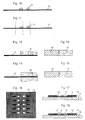
- the invention is an anode conductor from a metal powder paste completely bordered so that the anode arrester only on one side from one out of the metal powder paste Drying and sintering protrude anode body 20 can, as initially seen in Figs. 22 and 23 in side view or top view is shown.
- Arrangement can use a multi-stage stencil process be in the first between two shadow masks 13, 14 strips 15 of tantalum foil or tantalum sheet with one Thickness of 50 to 150 microns can be placed.
- 16 shows one Top view of the shadow mask 13 with the strips 15 while 17 is a side view of the shadow masks 13, 14 with the Strip 15 is shown on a first base plate 16.
- the portion of the strip 15 that is in the hole of the shadow mask 13, 14 protrudes, can be supported by a spacer 17 (see Fig. 17). This spacer 17 can optionally also be part of the base plate 16 or on it be fixed.
- a doctored paste 18 (see Fig. 18)
- a further base plate 19 is placed on it (see FIG. 19), the first base plate 16 with the spacers 17 removed (see Fig. 20), and it becomes metal powder paste a second time squeegee (see Fig. 21).
- a strip of tantalum foil or tantalum sheet with a thickness of 50 to 150 microns with a paste from a To encapsulate binder system and a tantalum powder or to cast around. After molding, the so obtained is Anode body dried and sintered. In this way individual anode bodies are made with an anode arrester Tantalum foil or tantalum sheet according to Fig. 22 (side view) and 23 (top view) obtained in the above explained manner are treated further.
- anode body a paste consisting of a binder system and tantalum powder, prefabricated an elastic, film-like mass (green film) which are cut and made with the tantalum foil or glued to the tantalum sheet with a thickness of 50 to 150 microns becomes. After drying and sintering, individual Anode body with an anode conductor made of tantalum foil or Tantalum sheet obtained as shown in FIGS. 22 and 23 are.
Landscapes
- Engineering & Computer Science (AREA)
- Power Engineering (AREA)
- Microelectronics & Electronic Packaging (AREA)
- Chemical & Material Sciences (AREA)
- Materials Engineering (AREA)
- Fixed Capacitors And Capacitor Manufacturing Machines (AREA)
- Powder Metallurgy (AREA)
- Electric Double-Layer Capacitors Or The Like (AREA)
- Electrolytic Production Of Non-Metals, Compounds, Apparatuses Therefor (AREA)
- Silicon Compounds (AREA)
- Secondary Cells (AREA)
- Battery Electrode And Active Subsutance (AREA)
- Networks Using Active Elements (AREA)
- Thermistors And Varistors (AREA)
Abstract
Description
- Fig. 1 bis 3
- schematische Darstellungen zur Erläuterung eines ersten Ausführungsbeispiels der Erfindung,
- Fig. 4 bis 6
- schematische Darstellungen zur Erläuterung eines zweiten Ausführungsbeispiels der Erfindung,
- Fig. 7 bis 13
- schematische Darstellungen zur Erläuterung eines ersten Verfahrens zum Herstellen eines Anodenkörpers,
- Fig. 14 und 15
- schematische Darstellungen zur Erläuterung einer Abwandlung des Verfahrens nach den Fig. 7 bis 13,
- Fig. 16 bis 23
- schematische Darstellungen zur Erläuterung eines zweiten Verfahrens zum Herstellen eines Anodenkörpers und
- Fig. 24 bis 26
- schematische Darstellungen zur Erläuterung eines herkömmlichen Chipkondensators.
Claims (23)
- Anode für einen Elektrolyt-Kondensator mit einem Anodenkörper (1; 20) einer fest vorgegebenen Form und mit einem flächigen Anodenableiter (9), bei der der Anodenkörper (1; 20) aus einem kontinuierlich verformbaren Material, das verfestigt werden kann, an den Anodenableiter (9) angeformt ist.
- Anode nach Anspruch 1,
bei der der Anodenkörper (1; 20) einen Endabschnitt des Anodenableiters (9) vollständig umschließt. - Anode nach Anspruch 1 oder 2,
bei der der Anodenkörper (1; 20) aus einem offenporigen Sinterkörper besteht. - Anode nach Anspruch 3,
bei der der Sinterkörper aus einem geeigneten Metall wie Tantal oder Niob oder einer geeigneten Metall-Legierung oder einem anderen zur Ausbildung eines Dielektrikums fähigen Material hergestellt ist. - Anode nach einem der Ansprüche 1 bis 4,
bei der der Anodenableiter (9) aus einem geeigneten Metall wie Tantal oder Niob oder einer geeigneten Metall-Legierung oder einem anderen zur Ausbildung eines Dielektrikums fähigen Material hergestellt ist. - Anode nach einem der Ansprüche 1 bis 5,
bei der der Anodenableiter (9) die Form eines Blechstreifens mit einem Verhältnis Breite/Dicke zwischen 2 und 100 aufweist. - Kondensator mit einer Anode nach Anspruch 1 bis 6,
bei dem der Anodenkörper (1; 20) von einem Dielektrikum (2) umgeben ist, bei dem auf dem Dielektrikum (2) eine Schichtkathode (3) vorgesehen ist, bei dem ein weiterer Endabschnitt des Anodenableiters (9) zu einer ersten Anschlußlasche geformt ist und bei dem die Schichtkathode (3) mit einer zweiten Anschlußlasche verbunden ist. - Verfahren zur Herstellung einer Anode nach einem der Ansprüche 1 bis 6,
wobei ein kontinuierlich verformbares Material, das verfestigt werden kann, unter gleichzeitiger äußerer Formgebung an einen flächigen Anodenableiter (9) angeformt und anschließend zur Bildung eines Anodenkörpers (1; 20) verfestigt wird. - Verfahren nach Anspruch 8,
wobei eine Paste (18) aus einem Bindersystem und einem Pulver auf den Anodenableiter (9) aufgetragen und sodann getrocknet und gesintert wird. - Verfahren nach Anspruch 9,
wobei die Paste (18) unter Verwendung einer Schablone (11) durch Drucken aufgetragen wird. - Verfahren nach Anspruch 9,
wobei die Paste (18) durch Siebdrucken aufgetragen wird. - Verfahren nach einem der Ansprüche 9 bis 11,
wobei die Paste (18) beidseitig auf den Anodenableiter (9) aufgetragen wird. - Verfahren nach Anspruch 9,
wobei die Paste (18) mittels zweier Masken, von denen jede jeweils einer Seite des Anodenableiters (9) zugeordnet ist, auf den Anodenableiter (9) aufgetragen wird. - Verfahren nach Anspruch 13,
wobei ein einen Rand eines Loches der Maske überragendes Ende des Anodenableiters (9) mit einem Abstandhalter (17) abgestützt wird. - Verfahren nach Anspruch 9,
wobei die Paste (18) durch Umspritzen, Umpressen oder Umgießen auf den Anodenableiter (9) aufgetragen wird. - Verfahren nach Anspruch 9,
wobei aus der Paste (18) eine Grünfolie gefertigt wird, die zugeschnitten und mit dem Anodenableiter (9) verklebt wird. - Verfahren nach Anspruch 8,
wobei der Anodenableiter (9) mit einem Pulver umpreßt wird, so daß ein Preßling entsteht, aus dem der Anodenableiter (9) an einer Seite herausragt, und wobei der Preßling anschließend gesintert wird. - Verfahren nach Anspruch 17,
wobei der flächige Anodenableiter (9) vor dem Pressen in eine Pulverschüttung des Pulvers eingeschoben wird. - Verfahren nach Anspruch 17 oder 18,
wobei für den Anodenableiter (9) ein streifenförmiges Blech mit einem Verhältnis Breite/Dicke zwischen 2 und 100 verwendet wird. - Verfahren nach Anspruch 17 bis 19,
wobei für den Anodenableiter (9) eine Tantalfolie oder ein Tantalblech (10) vorgesehen wird. - Verfahren nach Anspruch 17 bis 20,
wobei für das Pulver ein Tantalpulver vorgesehen wird. - Verfahren nach einem der Ansprüche 17 bis 21,
wobei dem Pulver ein Additiv mit Schmierwirkung, insbesondere Campher, beigefügt wird. - Verfahren nach Anspruch 22,
wobei das Additiv vor dem Sintern entfernt wird.
Applications Claiming Priority (3)
| Application Number | Priority Date | Filing Date | Title |
|---|---|---|---|
| DE19941094 | 1999-08-30 | ||
| DE19941094A DE19941094A1 (de) | 1999-08-30 | 1999-08-30 | Kondensator und Verfahren zum Herstellen eines Anodenkörpers und eines Anodenableiters hierfür |
| EP00960356A EP1208573B1 (de) | 1999-08-30 | 2000-08-21 | Anode für elektrolytkondensatoren, elektrolyt-kondensator und verfahren zur herstellung der anode |
Related Parent Applications (1)
| Application Number | Title | Priority Date | Filing Date |
|---|---|---|---|
| EP00960356A Division EP1208573B1 (de) | 1999-08-30 | 2000-08-21 | Anode für elektrolytkondensatoren, elektrolyt-kondensator und verfahren zur herstellung der anode |
Publications (2)
| Publication Number | Publication Date |
|---|---|
| EP1477998A2 true EP1477998A2 (de) | 2004-11-17 |
| EP1477998A3 EP1477998A3 (de) | 2007-09-05 |
Family
ID=7920074
Family Applications (2)
| Application Number | Title | Priority Date | Filing Date |
|---|---|---|---|
| EP04017526A Withdrawn EP1477998A3 (de) | 1999-08-30 | 2000-08-21 | Anode für Elektrolytkondensatoren, Elektrolytkondensator und Verfahren zur Herstellung der Anode |
| EP00960356A Expired - Lifetime EP1208573B1 (de) | 1999-08-30 | 2000-08-21 | Anode für elektrolytkondensatoren, elektrolyt-kondensator und verfahren zur herstellung der anode |
Family Applications After (1)
| Application Number | Title | Priority Date | Filing Date |
|---|---|---|---|
| EP00960356A Expired - Lifetime EP1208573B1 (de) | 1999-08-30 | 2000-08-21 | Anode für elektrolytkondensatoren, elektrolyt-kondensator und verfahren zur herstellung der anode |
Country Status (18)
| Country | Link |
|---|---|
| US (3) | US6493213B1 (de) |
| EP (2) | EP1477998A3 (de) |
| JP (1) | JP2003508907A (de) |
| KR (1) | KR100730916B1 (de) |
| CN (1) | CN1258786C (de) |
| AT (1) | ATE282244T1 (de) |
| AU (1) | AU7269300A (de) |
| BR (1) | BR0013708A (de) |
| CA (1) | CA2379305A1 (de) |
| CZ (1) | CZ2002701A3 (de) |
| DE (4) | DE19941094A1 (de) |
| HU (1) | HUP0202307A2 (de) |
| IL (2) | IL147352A0 (de) |
| MX (1) | MXPA02002153A (de) |
| NO (1) | NO20021016D0 (de) |
| PT (1) | PT1208573E (de) |
| TW (1) | TW455894B (de) |
| WO (1) | WO2001016973A1 (de) |
Families Citing this family (21)
| Publication number | Priority date | Publication date | Assignee | Title |
|---|---|---|---|---|
| DE19941094A1 (de) * | 1999-08-30 | 2003-07-10 | Epcos Ag | Kondensator und Verfahren zum Herstellen eines Anodenkörpers und eines Anodenableiters hierfür |
| DE10057488B4 (de) * | 2000-11-20 | 2006-05-24 | Epcos Ag | Kondensator |
| DE10131236B4 (de) * | 2001-06-28 | 2006-03-30 | Epcos Ag | Kondensator |
| DE10244713A1 (de) * | 2002-07-18 | 2004-02-05 | Epcos Ag | Oberflächenmontierbares Bauelement und Verfahren zu dessen Herstellung |
| TWI226648B (en) | 2002-07-18 | 2005-01-11 | Epcos Ag | Surface-mountable component and its production method |
| WO2004111288A2 (en) * | 2003-06-12 | 2004-12-23 | Sunel Technologies, Llc | Fabrication of titanium and titanium alloy anode for dielectric and insulated films |
| US20040264704A1 (en) * | 2003-06-13 | 2004-12-30 | Camille Huin | Graphical user interface for determining speaker spatialization parameters |
| US20080106853A1 (en) * | 2004-09-30 | 2008-05-08 | Wataru Suenaga | Process for Producing Porous Sintered Metal |
| DE102005007583A1 (de) * | 2005-02-18 | 2006-08-24 | Epcos Ag | Verfahren zur Herstellung eines Anodenkörpers und Anodenkörper |
| DE102005007582A1 (de) * | 2005-02-18 | 2006-08-24 | Epcos Ag | Kondensator mit einem niedrigen Ersatzserienwiderstand und Kondensatoranordung |
| US7554792B2 (en) * | 2007-03-20 | 2009-06-30 | Avx Corporation | Cathode coating for a wet electrolytic capacitor |
| US7460356B2 (en) * | 2007-03-20 | 2008-12-02 | Avx Corporation | Neutral electrolyte for a wet electrolytic capacitor |
| US7649730B2 (en) * | 2007-03-20 | 2010-01-19 | Avx Corporation | Wet electrolytic capacitor containing a plurality of thin powder-formed anodes |
| CN101345139B (zh) * | 2007-07-12 | 2011-10-05 | 电子科技大学 | 一种固体钽电解电容器及其制造方法 |
| JP4999673B2 (ja) * | 2007-12-25 | 2012-08-15 | ニチコン株式会社 | 固体電解コンデンサ素子およびその製造方法 |
| DE102008063853B4 (de) | 2008-12-19 | 2012-08-30 | H.C. Starck Gmbh | Kondensatoranode |
| US8218292B2 (en) * | 2009-07-31 | 2012-07-10 | Avx Corporation | Dry powder stencil printing of solid electrolytic capacitor components |
| US8139344B2 (en) * | 2009-09-10 | 2012-03-20 | Avx Corporation | Electrolytic capacitor assembly and method with recessed leadframe channel |
| DE102011116939A1 (de) | 2011-10-26 | 2013-05-02 | H.C. Starck Gmbh | Verzugsfreie schablonengedruckte Anoden auf Ta-/Nb-Blech |
| US8675349B2 (en) * | 2011-12-14 | 2014-03-18 | Kennet Electronics Corporation | Stack capacitor having high volumetric efficiency |
| WO2018136380A1 (en) * | 2017-01-17 | 2018-07-26 | Kemet Electronics Corporation | Improved wire to anode connection |
Family Cites Families (23)
| Publication number | Priority date | Publication date | Assignee | Title |
|---|---|---|---|---|
| DE215420C (de) | ||||
| US3465426A (en) * | 1966-05-02 | 1969-09-09 | Mallory & Co Inc P R | Powder on foil capacitor |
| US3412444A (en) * | 1966-05-02 | 1968-11-26 | Mallory & Co Inc P R | Method for making capacitor having porous electrode of sintered powder on foil |
| US3579813A (en) | 1968-12-23 | 1971-05-25 | Matsuo Electric Co | Method of making electronic components on comblike metal fingers and severing the fingers |
| US3903589A (en) | 1972-01-31 | 1975-09-09 | Mallory & Co Inc P R | Method for fabrication of anodes |
| GB2110878B (en) * | 1981-12-01 | 1986-02-05 | Standard Telephones Cables Ltd | Batch process for making capacitors |
| JPS5934625A (ja) * | 1982-08-20 | 1984-02-25 | 松尾電機株式会社 | チツプ型固体電解コンデンサの製造方法 |
| DD215420A1 (de) * | 1983-05-11 | 1984-11-07 | Teltow Elektronik Forschzent | Verfahren zur herstellung eines tantal-chip-kondensators |
| US4603467A (en) * | 1984-05-25 | 1986-08-05 | Marcon Electronics Co., Ltd. | Method of manufacturing chip-type aluminum electrolytic capacitor |
| US4544403A (en) * | 1984-11-30 | 1985-10-01 | Fansteel Inc. | High charge, low leakage tantalum powders |
| DD244926B1 (de) * | 1985-10-04 | 1988-11-23 | Hermsdorf Keramik Veb | Zweiseitiges pressverfahren zur herstellung von sinteranoden fuer festelektrolytkondensatoren |
| US4660127A (en) * | 1985-12-17 | 1987-04-21 | North American Philips Corporation | Fail-safe lead configuration for polar SMD components |
| FR2602907B1 (fr) * | 1986-08-05 | 1988-11-25 | Sprague France | Anode de condensateur, procede de fabrication de cette anode, et condensateur la comportant |
| FR2625602B1 (fr) * | 1987-12-30 | 1994-07-01 | Europ Composants Electron | Procede de fabrication de condensateurs electrolytiques a l'aluminium et condensateur a anode integree obtenu par ce procede |
| US5001607A (en) * | 1989-11-13 | 1991-03-19 | Tansistor Electronics, Inc. | Tantalum capacitor with non-contiguous cathode elements and method for making |
| US5122931A (en) * | 1989-12-27 | 1992-06-16 | Nippon Chemi-Con Corporation | Solid electrolytic capacitor and a method of producing the same |
| JPH0787171B2 (ja) * | 1990-04-06 | 1995-09-20 | ローム株式会社 | 固体電解コンデンサの製造方法 |
| US5357399A (en) | 1992-09-25 | 1994-10-18 | Avx Corporation | Mass production method for the manufacture of surface mount solid state capacitor and resulting capacitor |
| DE19525143A1 (de) * | 1995-07-11 | 1997-01-16 | Biotronik Mess & Therapieg | Elektrolytkondensator, insbesondere Tantal-Elektrolytkondensator |
| WO1998028805A1 (en) * | 1996-12-23 | 1998-07-02 | Aer Energy Resources, Inc. | Mercury-free zinc anode for electrochemical cell and method for making same |
| JP3233084B2 (ja) * | 1997-11-06 | 2001-11-26 | 日本電気株式会社 | 固体電解コンデンサの陽極体の製造方法 |
| DE19927909A1 (de) * | 1998-09-10 | 2000-03-16 | Starck H C Gmbh Co Kg | Paste zur Herstellung von gesinterten Refraktärmetallschichten, insbesondere Erdsäuremetall-Elektrolytkondensatoren oder -anoden |
| DE19941094A1 (de) * | 1999-08-30 | 2003-07-10 | Epcos Ag | Kondensator und Verfahren zum Herstellen eines Anodenkörpers und eines Anodenableiters hierfür |
-
1999
- 1999-08-30 DE DE19941094A patent/DE19941094A1/de not_active Withdrawn
-
2000
- 2000-08-21 AT AT00960356T patent/ATE282244T1/de not_active IP Right Cessation
- 2000-08-21 IL IL14735200A patent/IL147352A0/xx active IP Right Grant
- 2000-08-21 EP EP04017526A patent/EP1477998A3/de not_active Withdrawn
- 2000-08-21 DE DE10040853A patent/DE10040853A1/de not_active Withdrawn
- 2000-08-21 MX MXPA02002153A patent/MXPA02002153A/es active IP Right Grant
- 2000-08-21 HU HU0202307A patent/HUP0202307A2/hu unknown
- 2000-08-21 JP JP2001520427A patent/JP2003508907A/ja not_active Withdrawn
- 2000-08-21 EP EP00960356A patent/EP1208573B1/de not_active Expired - Lifetime
- 2000-08-21 AU AU72693/00A patent/AU7269300A/en not_active Abandoned
- 2000-08-21 CN CNB008122482A patent/CN1258786C/zh not_active Expired - Fee Related
- 2000-08-21 WO PCT/DE2000/002845 patent/WO2001016973A1/de not_active Ceased
- 2000-08-21 DE DE10082598T patent/DE10082598D2/de not_active Expired - Lifetime
- 2000-08-21 PT PT00960356T patent/PT1208573E/pt unknown
- 2000-08-21 CZ CZ2002701A patent/CZ2002701A3/cs unknown
- 2000-08-21 KR KR1020027002599A patent/KR100730916B1/ko not_active Expired - Fee Related
- 2000-08-21 CA CA002379305A patent/CA2379305A1/en not_active Abandoned
- 2000-08-21 BR BR0013708-1A patent/BR0013708A/pt not_active IP Right Cessation
- 2000-08-21 DE DE50008616T patent/DE50008616D1/de not_active Expired - Fee Related
- 2000-08-29 TW TW089117476A patent/TW455894B/zh not_active IP Right Cessation
- 2000-08-30 US US09/651,600 patent/US6493213B1/en not_active Expired - Lifetime
-
2001
- 2001-12-27 IL IL147352A patent/IL147352A/en not_active IP Right Cessation
-
2002
- 2002-02-20 US US10/079,113 patent/US6699431B2/en not_active Expired - Lifetime
- 2002-02-28 NO NO20021016A patent/NO20021016D0/no unknown
-
2003
- 2003-12-24 US US10/746,185 patent/US20040136857A1/en not_active Abandoned
Also Published As
| Publication number | Publication date |
|---|---|
| TW455894B (en) | 2001-09-21 |
| NO20021016L (no) | 2002-02-28 |
| EP1208573A1 (de) | 2002-05-29 |
| EP1477998A3 (de) | 2007-09-05 |
| AU7269300A (en) | 2001-03-26 |
| KR100730916B1 (ko) | 2007-06-22 |
| CA2379305A1 (en) | 2001-03-08 |
| DE10040853A1 (de) | 2001-04-26 |
| WO2001016973A1 (de) | 2001-03-08 |
| NO20021016D0 (no) | 2002-02-28 |
| DE10082598D2 (de) | 2002-08-14 |
| HUP0202307A2 (en) | 2002-10-28 |
| CZ2002701A3 (cs) | 2002-09-11 |
| US20040136857A1 (en) | 2004-07-15 |
| US20020075628A1 (en) | 2002-06-20 |
| CN1258786C (zh) | 2006-06-07 |
| PT1208573E (pt) | 2005-03-31 |
| MXPA02002153A (es) | 2002-09-18 |
| KR20020027594A (ko) | 2002-04-13 |
| DE19941094A1 (de) | 2003-07-10 |
| DE50008616D1 (de) | 2004-12-16 |
| US6699431B2 (en) | 2004-03-02 |
| ATE282244T1 (de) | 2004-11-15 |
| EP1208573B1 (de) | 2004-11-10 |
| JP2003508907A (ja) | 2003-03-04 |
| US6493213B1 (en) | 2002-12-10 |
| CN1371522A (zh) | 2002-09-25 |
| IL147352A (en) | 2006-04-10 |
| BR0013708A (pt) | 2002-05-07 |
| IL147352A0 (en) | 2002-08-14 |
Similar Documents
| Publication | Publication Date | Title |
|---|---|---|
| EP1208573B1 (de) | Anode für elektrolytkondensatoren, elektrolyt-kondensator und verfahren zur herstellung der anode | |
| DE19738149B4 (de) | Fest-Elektrolytkondensatoranordnung und Verfahren zur Herstellung derselbigen | |
| DE69636710T2 (de) | Festelektrolytkondensator und dessen herstellungsverfahren | |
| DE4091418C2 (de) | Verfahren zur Herstellung eines Mehrschichtkondensators | |
| DE60019592T2 (de) | Festelektrolytkondensatoren und herstellungsverfahren | |
| DE10060653A1 (de) | Elektrischer Doppelschicht-Kondensator | |
| EP0249277B1 (de) | Passives elektrisches Bauelement | |
| DE10057488B4 (de) | Kondensator | |
| DE69935767T2 (de) | Metallisches elektrodenmaterial, dieses verwendender kondensator und herstellungsverfahren | |
| DE4312409B4 (de) | Einstellbarer Kondensator | |
| DE4423561C2 (de) | Oberflächenmontage-Elektronikbauteil mit Schmelzsicherung und entsprechendes Herstellungsverfahren | |
| DE60211628T2 (de) | Zusammengesetzte elektronische bauteile | |
| DE2835022C2 (de) | Anodenkörper für einen Festelektrolytkondensator | |
| DE10131236B4 (de) | Kondensator | |
| EP1445795B1 (de) | Verfahren zum Herstellen von Schaltungsträgern mit integrierten passiven Bauelementen | |
| DE69632883T2 (de) | Dielektrisches Material für einen Kondensator und Herstellungsverfahren | |
| EP4112582A1 (de) | Thermal interface material, energiespeicher mit einem thermal interface material und verfahren zu deren herstellung | |
| EP1386334A1 (de) | Keramisches vielschichtbauelement und verfahren zur herstellung | |
| EP0024302A2 (de) | Trockenelektrolyt-Kondensator | |
| WO2006105766A1 (de) | Anode für einen festelektrolytkondensator | |
| WO2019175090A1 (de) | Verfahren zur herstellung einer leiterplatte unter verwendung einer form für leiterelemente | |
| DE69009580T2 (de) | Verbindungsband für Anoden von elektrolytischen Kondensatoren sowie Verfahren zur Herstellung von elektrolytischen Kondensatoren unter Verwendung dieses Bandes. | |
| DE112022004266T5 (de) | Verbesserte vorrichtung und herstellungsverfahren von membran-kondensator-vorrichtungen | |
| DE10145362C2 (de) | Verfahren zur Herstellung eines keramischen Substrats | |
| EP1113712B1 (de) | Verfahren zum Herstellen von Leiterbahnen |
Legal Events
| Date | Code | Title | Description |
|---|---|---|---|
| PUAI | Public reference made under article 153(3) epc to a published international application that has entered the european phase |
Free format text: ORIGINAL CODE: 0009012 |
|
| AC | Divisional application: reference to earlier application |
Ref document number: 1208573 Country of ref document: EP Kind code of ref document: P |
|
| AK | Designated contracting states |
Kind code of ref document: A2 Designated state(s): AT BE CH CY DE DK ES FI FR GB GR IE IT LI LU MC NL PT SE |
|
| PUAL | Search report despatched |
Free format text: ORIGINAL CODE: 0009013 |
|
| RAP1 | Party data changed (applicant data changed or rights of an application transferred) |
Owner name: KEMET ELECTRONICS CORPORATION |
|
| AK | Designated contracting states |
Kind code of ref document: A3 Designated state(s): AT BE CH CY DE DK ES FI FR GB GR IE IT LI LU MC NL PT SE |
|
| RIC1 | Information provided on ipc code assigned before grant |
Ipc: H01G 9/052 20060101ALI20070730BHEP Ipc: H01G 9/012 20060101ALI20070730BHEP Ipc: H01G 9/15 20060101AFI20070730BHEP |
|
| AKX | Designation fees paid | ||
| STAA | Information on the status of an ep patent application or granted ep patent |
Free format text: STATUS: THE APPLICATION IS DEEMED TO BE WITHDRAWN |
|
| 18D | Application deemed to be withdrawn |
Effective date: 20080303 |
|
| REG | Reference to a national code |
Ref country code: DE Ref legal event code: 8566 |