EP1478212A1 - Organische elektrolumineszenzanzeige und verfahren zur ihrer herstellung - Google Patents
Organische elektrolumineszenzanzeige und verfahren zur ihrer herstellung Download PDFInfo
- Publication number
- EP1478212A1 EP1478212A1 EP03795293A EP03795293A EP1478212A1 EP 1478212 A1 EP1478212 A1 EP 1478212A1 EP 03795293 A EP03795293 A EP 03795293A EP 03795293 A EP03795293 A EP 03795293A EP 1478212 A1 EP1478212 A1 EP 1478212A1
- Authority
- EP
- European Patent Office
- Prior art keywords
- organic
- insulating film
- electrode
- organic electroluminescence
- electroluminescence device
- Prior art date
- Legal status (The legal status is an assumption and is not a legal conclusion. Google has not performed a legal analysis and makes no representation as to the accuracy of the status listed.)
- Withdrawn
Links
Images



Classifications
-
- H—ELECTRICITY
- H10—SEMICONDUCTOR DEVICES; ELECTRIC SOLID-STATE DEVICES NOT OTHERWISE PROVIDED FOR
- H10K—ORGANIC ELECTRIC SOLID-STATE DEVICES
- H10K59/00—Integrated devices, or assemblies of multiple devices, comprising at least one organic light-emitting element covered by group H10K50/00
- H10K59/10—OLED displays
- H10K59/12—Active-matrix OLED [AMOLED] displays
- H10K59/125—Active-matrix OLED [AMOLED] displays including organic TFTs [OTFT]
-
- H—ELECTRICITY
- H05—ELECTRIC TECHNIQUES NOT OTHERWISE PROVIDED FOR
- H05B—ELECTRIC HEATING; ELECTRIC LIGHT SOURCES NOT OTHERWISE PROVIDED FOR; CIRCUIT ARRANGEMENTS FOR ELECTRIC LIGHT SOURCES, IN GENERAL
- H05B33/00—Electroluminescent light sources
- H05B33/12—Light sources with substantially two-dimensional [2D] radiating surfaces
- H05B33/22—Light sources with substantially two-dimensional [2D] radiating surfaces characterised by the chemical or physical composition or the arrangement of auxiliary dielectric or reflective layers
-
- H—ELECTRICITY
- H05—ELECTRIC TECHNIQUES NOT OTHERWISE PROVIDED FOR
- H05B—ELECTRIC HEATING; ELECTRIC LIGHT SOURCES NOT OTHERWISE PROVIDED FOR; CIRCUIT ARRANGEMENTS FOR ELECTRIC LIGHT SOURCES, IN GENERAL
- H05B33/00—Electroluminescent light sources
- H05B33/10—Apparatus or processes specially adapted to the manufacture of electroluminescent light sources
-
- H—ELECTRICITY
- H05—ELECTRIC TECHNIQUES NOT OTHERWISE PROVIDED FOR
- H05B—ELECTRIC HEATING; ELECTRIC LIGHT SOURCES NOT OTHERWISE PROVIDED FOR; CIRCUIT ARRANGEMENTS FOR ELECTRIC LIGHT SOURCES, IN GENERAL
- H05B33/00—Electroluminescent light sources
- H05B33/12—Light sources with substantially two-dimensional [2D] radiating surfaces
- H05B33/14—Light sources with substantially two-dimensional [2D] radiating surfaces characterised by the chemical or physical composition or the arrangement of the electroluminescent material, or by the simultaneous addition of the electroluminescent material in or onto the light source
-
- H—ELECTRICITY
- H05—ELECTRIC TECHNIQUES NOT OTHERWISE PROVIDED FOR
- H05B—ELECTRIC HEATING; ELECTRIC LIGHT SOURCES NOT OTHERWISE PROVIDED FOR; CIRCUIT ARRANGEMENTS FOR ELECTRIC LIGHT SOURCES, IN GENERAL
- H05B33/00—Electroluminescent light sources
- H05B33/12—Light sources with substantially two-dimensional [2D] radiating surfaces
- H05B33/26—Light sources with substantially two-dimensional [2D] radiating surfaces characterised by the composition or arrangement of the conductive material used as an electrode
-
- H—ELECTRICITY
- H10—SEMICONDUCTOR DEVICES; ELECTRIC SOLID-STATE DEVICES NOT OTHERWISE PROVIDED FOR
- H10K—ORGANIC ELECTRIC SOLID-STATE DEVICES
- H10K10/00—Organic devices specially adapted for rectifying, amplifying, oscillating or switching; Organic capacitors or resistors having potential barriers
- H10K10/40—Organic transistors
- H10K10/46—Field-effect transistors, e.g. organic thin-film transistors [OTFT]
- H10K10/462—Insulated gate field-effect transistors [IGFETs]
- H10K10/466—Lateral bottom-gate IGFETs comprising only a single gate
-
- H—ELECTRICITY
- H10—SEMICONDUCTOR DEVICES; ELECTRIC SOLID-STATE DEVICES NOT OTHERWISE PROVIDED FOR
- H10K—ORGANIC ELECTRIC SOLID-STATE DEVICES
- H10K10/00—Organic devices specially adapted for rectifying, amplifying, oscillating or switching; Organic capacitors or resistors having potential barriers
- H10K10/80—Constructional details
- H10K10/88—Passivation; Containers; Encapsulations
-
- H—ELECTRICITY
- H10—SEMICONDUCTOR DEVICES; ELECTRIC SOLID-STATE DEVICES NOT OTHERWISE PROVIDED FOR
- H10K—ORGANIC ELECTRIC SOLID-STATE DEVICES
- H10K59/00—Integrated devices, or assemblies of multiple devices, comprising at least one organic light-emitting element covered by group H10K50/00
- H10K59/10—OLED displays
- H10K59/12—Active-matrix OLED [AMOLED] displays
- H10K59/123—Connection of the pixel electrodes to the thin film transistors [TFT]
Definitions
- the present invention relates to an organic electroluminescence display having a display array or a regular arrangement of a plurality of light emitting parts which consist of organic electroluminescence devices each having a light-emitting layer made of a thin film of organic electroluminescence material utilizing electroluminescence (hereinafter, also referred to as EL) of organic compound material in which luminescence is produced by electron or hole injection.
- EL electroluminescence
- An organic EL display comprising a plurality of organic EL devices arranged in a matrix, is receiving attention as a display that is low in power consumption, high in display quality, and capable of low-profile configuration.
- the organic EL device is known as a self-luminescence device in which at least one organic material layer and a metal electrode are laminated on a transparent substrate.
- An example of the transparent substrate is a glass plate provided with a transparent electrode of indium-tin oxide, i.e., so-called ITO.
- Examples of the organic material layer include an organic electron-transporting layer, an organic light-emitting layer, and an organic hole-transporting layer.
- Positive and negative voltages are respectively applied to the transparent electrode and the metal electrode, i.e., anode and cathode, for charge accumulation.
- a barrier voltage i.e., a luminescence threshold voltage inherent to the device is exceeded, a current starts to flow and there occurs luminescence with certain intensity approximately proportional to this direct current.
- display panels that use organic EL devices are a simple matrix type display panel in which the organic EL devices are simply arranged in a matrix, and an active matrix type display panel in which the organic EL devices arranged in a matrix are provided with an additional transistor-based driving element each.
- the active matrix type display panel has such advantages as low power consumption and low interpixel crosstalk.
- the active matrix type display is suited to large-screen display and high-definition display in particular.
- the display of active matrix drive system exercises switching with respect to each of the light emitting parts by using thin film transistors (TFTs) which are made of polysilicon, for example. Consequently, a current is supplied pixel by pixel to cause luminescence of the organic EL devices.
- TFTs thin film transistors
- MOS-FETs Metal Oxide Semiconductor Field Effect Transistors
- a MOS-FET has two reverse conductive regions of polysilicon which are formed on a glass substrate, for example.
- An oxide (SiO 2 ) thin film and a metal gate electrode are formed in succession on the surface of the substrate, between the reverse conductive regions, so that the conductivity is controlled by the field applied from the metal gate electrode. Since the display substrate must be a polysilicon substrate or the like which requires a high temperature treatment, and films of inorganic material such as Si must be formed thereon, the fabrication involves high temperature process.
- Displays having large-screen display panels are in high demand.
- a low-temperature polysilicon substrate thereof Despite the name “low-temperature,” however, the substrate requires a heat treatment on the order of 500 °C at the time of fabrication.
- incorporating inorganic material TFTs into the large-screen display panel of an organic EL display of active matrix drive system inevitably pushes up the cost of the display.
- organic TFT that has an organic semiconductor film of organic material formed between a pair of opposite electrodes. It is considered that this organic TFT can be used to drive organic EL devices.
- An organic EL display comprises a substrate and a plurality of light emitting parts formed on the substrate, each of the light emitting parts including an organic EL device and an organic thin film transistor connected to the organic EL device.
- the organic EL device has a pair of opposed electrodes and an organic material layer including an organic light-emitting layer laminated between the pair of electrodes.
- the organic thin film transistor has a source electrode and a drain electrode opposed to each other, an organic semiconductor film laminated so as to form a channel between the source electrode and the drain electrode, and a gate electrode for applying a field to the organic semiconductor film between the source electrode and the drain electrode.
- Each of the light emitting parts further includes a source-drain insulating film for avoiding a short circuit between the source electrode and the drain electrode, a protective insulating film for protecting the organic semiconductor film, and a pixel insulating film for covering an edge of either one of the electrodes of the organic EL device. At least two out of the source-drain insulating film, the protective insulating film, and the pixel insulating film are made of the same dielectric material.
- a method of fabricating an organic EL display according to the present invention is one for fabricating an organic EL display comprising a substrate and a plurality of light emitting parts formed on the substrate, each of the light emitting parts including an organic EL device and an organic thin film transistor connected to the organic EL device.
- the method comprises: a step of forming organic thin film transistors each having a source electrode and a drain electrode opposed to each other, an organic semiconductor film laminated so as to form a channel between the source electrode and the drain electrode, and a gate electrode for applying a field to the organic semiconductor film between the source electrode and the drain electrode; a step of forming the organic EL devices each having a pair of opposed electrodes and an organic material layer including an organic light-emitting layer laminated between the pair of electrodes; and an insulating film forming step of forming, in each of the light emitting parts, a source-drain insulating film for avoiding a short circuit between the source electrode and the drain electrode, a protective insulating film for protecting the organic semiconductor film, and a pixel insulating film for covering an edge of either one of the electrodes of the organic EL device. At least two out of the source-drain insulating film, the protective insulating film, and the pixel insulating film are made of the same dielectric material, the two being formed in an
- Fig. 1 shows an organic EL display of active matrix drive system according to an embodiment.
- the display has a display panel 101, an address driver 110, a data driver 120, and a controller 130.
- the display panel 101 comprises "n" (n is an integer) scan lines SL1 to SLn which are formed in parallel at predetermined intervals, and "m" (m is an integer) data lines DL1 to DLm which are formed in parallel at predetermined intervals.
- the scan lines and the data lines are laid so that they cross each other at predetermined intervals with right angles therebetween.
- the display panel 101 also comprises n x m light emitting parts 102 which are formed at portions corresponding to the respective intersections of the scan lines and the data lines.
- Each scan line is connected to the address driver 110 at one end.
- Each data line is connected to the data driver 120 at one end.
- the address driver 110 applies a voltage to the scan lines SL1-SLn one by one in succession.
- the data driver 120 applies a data voltage for causing luminescence of the light emitting parts 102 to the data lines DL1-DLm.
- the controller 130 is connected with the address driver 110 and the data driver 120, and controls the operation of the address driver 110 and the data driver 120 according to image data supplied in advance.
- each of the light emitting parts 102 comprises an address organic TFT 11, a drive organic TFT 12, a capacitor 13, and an organic EL device 15.
- the address organic TFT 11 is a transistor for selection, and the drive organic TFT 12 a transistor for driving.
- the gate electrode G of the address organic TFT 11 is connected with the scan line SL to which an address signal is supplied.
- the drain electrode D of the address organic TFT 11 is connected with the data line DL to which a data signal is supplied.
- the source electrode S of the address organic TFT 11 is connected to the gate electrode G of the drive organic TFT 12 and one of the terminals of the capacitor 13.
- the source electrode S of the drive organic TFT 12 is connected to a power supply line VccL along with the other terminal of the capacitor 13.
- the drain electrode D of the drive organic TFT 12 is connected to the anode of the organic EL device 15.
- the cathode of the organic EL device 15 is connected to a common electrode 17.
- the power supply line VccL shown in Fig. 2 and the common electrode 17 in connection with the cathode of each organic EL device 15 are connected to a voltage source (not shown) for supplying power thereto.
- an ON voltage is supplied to the gate electrode G of the address organic TFT 11.
- the address organic TFT 11 passes a current from the source electrode S to the drain electrode D, the current corresponding to the voltage of the data supplied to the source electrode S.
- the gate electrode G of the address organic TFT 11 is supplied with an OFF voltage, the address organic TFT 11 reaches a so-called cutoff in which the drain electrode D of the address organic TFT 11 enters an open state. Consequently, while the gate electrode G of the address organic TFT 11 is at the ON voltage, the capacitor 13 is charged and the voltage is supplied to the gate electrode G of the drive organic TFT 12.
- the drive organic TFT 12 then passes a current based on the gate voltage and the source voltage, from the source electrode S to the drain electrode D. This makes the organic EL device 15 produce luminescence.
- the gate electrode G of the address organic TFT 11 is at the OFF voltage, the address organic TFT 11 enters an open state.
- the drive organic TFT 12 retains the voltage of the gate electrode G because of the charge stored in the capacitor 13, thus maintaining the driving current until the next scan.
- the luminescence of the organic EL device 15 is also maintained.
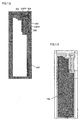
- Figs. 3 and 4 shows the structure of the organic EL display panel that comprises organic EL devices to be driven by the organic TFTs of the present invention.
- each single light emitting part of the organic EL display panel contains an organic EL device 15, a plurality of organic TFTs necessary for driving the organic EL device 15, such as an address organic TFT 11 and a drive organic TFT 12, and a capacitor 13 necessary for retaining the data voltage.
- This configuration can be arranged near the intersections of the scan lines SL, data lines DL, and power supply lines VccL to achieve the light emitting parts of respective pixels.
- Fig. 4 shows a section taken along the line A-B of Fig. 3.
- an organic TFT includes a source electrode S, a drain electrode D, an organic semiconductor film OSF, a gate electrode G, and a gate insulating film GIF.
- the source electrode S and the drain electrode D are opposed to each other.
- the organic semiconductor film OSF is made of an organic semiconductor laminated so as to form a channel between the source and drain electrodes.
- the gate electrode G applies an electric field to the organic semiconductor film OSF between the source electrode S and the drain electrode D.
- the gate insulating film GIF insulates the gate electrode G from the source electrode S and the drain electrode D.
- the gate insulating film GIF is formed so as to cover at least the gate electrode G and the transistor portions.
- the gate insulating film GIF has a through hole TH which is necessary for establishing wiring between the transistors. Films of the same dielectric material may be formed simultaneously so that they function as the gate insulating film GIF and the dielectric of the capacitor 13. Thus, as shown in Fig. 4, the gate insulating film GIF and the dielectric of the capacitor 13 are formed continuously.
- a source-drain insulating film SDI is formed all over the source electrode S and the drain electrode D. This aims to avoid a short circuit with the common electrode 17 of the organic EL device.
- the source-drain insulating film SDI also covers the organic semiconductor film OSF, thereby functioning as an organic semiconductor protective insulating film OSPF of the organic semiconductor film.
- the source-drain insulating film SDI further covers edges of a pixel electrode 15a of the organic EL device 15, thereby functioning as a pixel insulating film PIF.
- the drive organic TFT 12 is connected to the pixel electrode 15a.
- An organic material layer 15b of the organic EL device typically has a thickness as extremely small as on the order of 0.1 ⁇ m. The edges of the pixel electrode 15a are thus prone to a short circuit with the common electrode 17. This is desirably avoided by the provision of the pixel insulating film PIF which covers the edges of the pixel electrode 15a.
- the organic EL device 15 comprises the pixel electrode 15a, the organic material layer 15b, and the common electrode 17.
- the organic material layer 15b typically consists of a plurality of layers including a hole injecting layer, a hole-transporting layer, a light-emitting layer, an electron-transporting layer, and an electron injecting layer; nevertheless, what is indispensable is the light-emitting layer alone.
- the organic material layer 15b is colored pixel by pixel depending on the luminescent color. Excepting the light-emitting layer, those layers common to different colors, if any, may be formed over the entire surface as if the common electrode 17 is, instead of being formed pixel by pixel.
- At least either one of the pixel electrode 15a and the common electrode 17 must have light transmittance in order to output the EL emission to exterior.
- any two or more films may be formed simultaneously.
- the source-drain insulating film SDI, the pixel insulating film PIF, and the organic semiconductor protective insulating film OSPF three are formed at the same time.
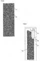
- Fig. 6 shows a structure for the case where the source-drain insulating film SDI and the pixel insulating film PIF are formed simultaneously.
- the formation of the organic semiconductor film OSF follows the simultaneous formation of the source-drain insulating film SDI and the pixel insulating film PIF. After the formation of the organic semiconductor film OSF, the organic semiconductor protective insulating film OSPF is formed.
- the foregoing example has dealt with two-transistor configuration which is the simplest to drive an organic EL device.
- the present invention may also be applied, however, to devices using three or more transistors.
- a bottom wiring pattern including a scan line SL and gate electrodes G is initially formed on a substrate 1 which is made of glass, plastic, or the like.
- the capacitor electrode 13a is arranged at a position directly below the power supply line to be connected with later. Arranging the capacitor directly below the power supply line allows a larger pixel area.
- the scan line SL and the gate electrodes are preferably made of low resistivity material, typically a pure metal or an alloy.
- the available materials include Al, Ag, Cu, Au, Cr, and alloys containing the same. Any method, including sputtering, EB (electron beam) evaporation, resistance heating evaporation, CVD (chemical vapor deposition), and printing may effect the film formation.
- the pattern formation may also use any method, such as photoetching, printing, and mask evaporation.
- conductive polymers may be used for the gate electrodes.
- the pattern formation may also be effected by low-cost methods such as printing.
- the gate insulating film GIF is formed in a predetermined pattern on the bottom wiring pattern.
- the dielectric layer 13b of the capacitor is simultaneously formed over the electrode 13a by using the same dielectric material as that of the gate insulating film GIF.
- the gate insulating film GIF is provided with a through hole TH for establishing connection between the gate electrode G of the address organic TFT and that of the drive organic TFT.
- a predetermined pattern of gate insulating film having portions of different thicknesses may be formed by performing a plurality of separate formation steps such as forming a thinner film in order to exercise the facilities of the gate insulating film GIF and the capacitor dielectric layer 13b, and forming a thicker film in order to ensure insulation between the power supply line and the scan line which intersect each other.
- the gate insulating film GIF is metal oxides, metal nitrides, metal fluorides, and other metal compounds, such as Al 2 O 3 , SiO 2 , SiN, and SiON, and insulative polymers such as polyimide.
- the film formation may be effected by any method, including sputtering, EB evaporation, resistance heating evaporation, CVD, printing, and spin coating.
- the pattern formation may also use any method, such as photoetching, printing, and mask evaporation.
- the pixel electrode 15a of approximately rectangular shape, serving as the anode of the organic EL device, is formed in a predetermined pattern on the gate insulating film GIF.
- the pixel electrode 15a is formed as an extremely thin semi-transparent film made of a pure metal or an alloy, or a transparent electrode made of metal oxide or the like.
- a pure metal or an alloy for example, semi-transparent films of Au, Pd, and the like, and transparent electrodes of ITO and the like are available.
- the pixel electrode 15a is typically made of a pure metal or an alloy.
- the available materials include Al, Ag, Cu, Au, Cr, and alloys containing the same.
- the film formation may be effected by any method, including sputtering, EB evaporation, resistance heating evaporation, CVD, and printing.
- the pattern formation may also use any method, such as photoetching, printing, and mask evaporation.
- the source electrodes S and drain electrodes D of the address organic TFT and drive organic TFT, and the data line DL and the power supply line VccL are formed in a predetermined wiring pattern on the pixel electrode 15a and the gate insulating film GIF.
- the data line DL and the power supply line VccL, parallel to each other across the pixel electrode 15a, are formed on the gate insulating film GIF so as to cross the scan line SL at right angles.
- part of the film of the power supply line VccL is simultaneously formed as the other electrode 13c of the capacitor which sandwiches the dielectric layer 13b with the electrode 13a of the capacitor.
- the power supply line VccL intended for power supply, is formed larger than the other lines in width. Since the resulting capacitor 13 is located immediately below the power supply line VccL, it is possible to secure a sufficient capacitance of the capacitor 13 without interfering with the pixel electrode.
- the capacitor 13 is arranged on a side of the drive organic TFT 12 opposite from the address organic TFT 11. The wiring length between the drive organic TFT 12 and the address organic TFT 11 thus becomes shorter than when the capacitor 13 is arranged between the drive organic TFT 12 and the address organic TFT 11. This also promises that the area of the pixel electrode is secured to improve the charge transfer speed.
- the source electrode S and the drain electrode D of the drive organic TFT in connection with the power supply line VccL are formed so as to overlap the corresponding gate electrode.
- the drain electrode D is connected to the pixel electrode 15a.
- the drain electrode D and the source electrode S of the address organic TFT in connection with the data line DL are formed so as to overlap the corresponding gate electrode.
- the source electrode S is connected to the gate electrode of the drive organic TFT via the through hole TH.
- the source electrodes and the drain electrodes are preferably made of material that allows efficient carrier injection to the intended organic semiconductor and has a low resistivity. Examples of the material include Au and Pd.
- the data line DL and the power supply line VccL are made of the same material as that of the scan line SL.
- the film formation may be effected by any method, including sputtering, EB evaporation, resistance heating evaporation, CVD, and printing.
- the pattern formation may also use any method, such as photoetching, printing, and mask evaporation.
- conductive polymers may be used for the source and drain electrodes.
- the pattern formation may also be effected by low-cost methods such as printing.
- the source electrodes and drain electrodes may be made of the same material as that of the pixel electrode 15a, in which case the pixel electrode 15a and the source and drain electrodes can be formed in a single step. Depending on the materials, the foregoing predetermined wiring pattern may be formed in a plurality of separate steps.
- the step of forming the pixel electrode 15a precedes the step of forming the source and drain electrodes.
- the steps may be performed in reverse order.
- the organic semiconductor film OSF is formed in a predetermined pattern so that it establishes connection with the source electrodes S, the drain electrodes D, and the gate insulating film GIF immediately above the gate electrodes of the drive organic TFT and the address organic TFT in connection with the power supply line VccL and the data line DL, respectively.
- the organic semiconductor film OSF is preferably made of material having high carrier mobility, such as low molecular organic semiconductor materials and organic semiconductor polymers.
- the film formation may be effected by any method, including sputtering, EB evaporation, resistance heating evaporation, CVD, printing, and spin coating.
- the pattern formation may also use any method, such as photoetching, printing, and mask evaporation.
- a common insulating film is formed in a predetermined pattern such that it overlaps the edges of the pixel electrode 15a of the organic EL device 15 and exposes the pixel electrode 15a.
- the common insulating film functions as the source-drain insulating film SDI, the pixel insulating film PIF, and the organic semiconductor protective insulating film OSPF.
- the common insulating film Among the available materials of the common insulating film are metal oxides, metal nitrides, metal fluorides, and other metal compounds, such as Al 2 O 3 , SiO 2 , SiN, and SiON, and insulative polymers such as polyimide.
- the film formation may be effected by any method, including sputtering, EB evaporation, resistance heating evaporation, CVD, printing, and spin coating.
- the pattern formation may also use any method, such as photoetching, printing, and mask evaporation.
- the underlying organic semiconductor film OSF is typically made of material that is poor in heat resistance, solvent resistance, and moisture resistance.
- the semiconductor film must be prevented from property deterioration in the process of forming the common insulating film which is formed on the organic semiconductor film.
- the organic material layer 15b including at least a light-emitting layer is formed on the pixel electrode 15a through the opening in the common insulating film. Aside from the light-emitting layer, the organic material layer 15b may include a hole injecting layer, a hole-transporting layer, an electron-transporting layer, an electron injection layer, and so on.
- the film formation may be effected by any method, including sputtering, EB evaporation, resistance heating evaporation, CVD, printing, and spin coating.
- the pattern formation may also use any method, such as photoetching, printing, and mask evaporation.
- the common electrode 17, i.e., the cathode of the organic EL device 15, is formed in a predetermined pattern on the organic material layer 15b.
- the common electrode 17 is made of a pure metal or an alloy.
- the available materials include Al, Ag, Cu, Au, Cr, and alloys thereof.
- the film formation may be effected by any method. For example, sputtering, EB evaporation, resistance heating evaporation, CVD, printing, and the like may be performed at temperatures not exceeding the glass transition temperatures of the respective organic material layers formed in the step of forming the organic material layers so as not to deteriorate any of the organic material layers.
- the pattern formation may also use any method, such as photoetching, printing, and mask evaporation.
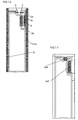
- the organic EL device 15 may be located over the organic TFTs 11 and 12.
- identical reference numerals or symbols designate the same members. Description thereof will thus be omitted.
- the common electrode 17 is desirably made of material having light transmittance. This structure has the advantage that the area of the organic EL device 15 can be increased for a higher opening ratio.
- the address organic TFT 11 and the drive organic TFT 12 are formed before a planarizing layer 20 is formed thereover except a connecting portion 19 to the pixel electrode 15a.
- the planarizing layer 20 functions as both the organic semiconductor protective insulating film OSPF and the source-drain insulating film SDI.
- the planarizing layer 20 is intended to cover projections and depressions resulting from the organic TFTs since the presence of the projections and depressions facilitates a short circuit between the pixel electrode 15a of the organic EL device and the common electrode 17. Since the underlying organic semiconductor materials are typically poor in heat resistance, solvent resistance, and moisture resistance, the semiconductor films must be protected from property deterioration in the process of forming the planarizing layer 20.
- the pixel electrode 15a is formed in connection with the drive organic TFT 12. Then, the organic material layer 15b and the common electrode 17 are formed to complete the display panel of the organic EL device according to the present invention.
- the members that require heat resistance, solvent resistance, and moisture resistance during the photolithography step and the like are previously formed before the evaporation of the organics. This precludes damage to the organic members which are poor in heat resistance, solvent resistance, and moisture resistance during the photolithography step and the like.
- at least two of the necessary insulating films can be formed simultaneously for simplified steps.
- the organic TFTs in the light emitting parts are organic thin film transistors of so-called MIS (Metal Insulator Semiconductor) type. Nevertheless, organic thin-film transistors of SIT (Static Induction Transistor) type may be used instead of MIS type.
- MIS Metal Insulator Semiconductor
- SIT Static Induction Transistor
Landscapes
- Engineering & Computer Science (AREA)
- Microelectronics & Electronic Packaging (AREA)
- Manufacturing & Machinery (AREA)
- Electroluminescent Light Sources (AREA)
- Thin Film Transistor (AREA)
- Devices For Indicating Variable Information By Combining Individual Elements (AREA)
- Formation Of Insulating Films (AREA)
Applications Claiming Priority (3)
| Application Number | Priority Date | Filing Date | Title |
|---|---|---|---|
| JP2002266449A JP4434563B2 (ja) | 2002-09-12 | 2002-09-12 | 有機el表示装置の製造方法 |
| JP2002266449 | 2002-09-12 | ||
| PCT/JP2003/011342 WO2004026004A1 (ja) | 2002-09-12 | 2003-09-05 | 有機エレクトロルミネッセンス表示装置及びその製造方法 |
Publications (2)
| Publication Number | Publication Date |
|---|---|
| EP1478212A1 true EP1478212A1 (de) | 2004-11-17 |
| EP1478212A4 EP1478212A4 (de) | 2009-09-16 |
Family
ID=31986641
Family Applications (1)
| Application Number | Title | Priority Date | Filing Date |
|---|---|---|---|
| EP03795293A Withdrawn EP1478212A4 (de) | 2002-09-12 | 2003-09-05 | Organische elektrolumineszenzanzeige und verfahren zur ihrer herstellung |
Country Status (8)
| Country | Link |
|---|---|
| US (1) | US7042163B2 (de) |
| EP (1) | EP1478212A4 (de) |
| JP (1) | JP4434563B2 (de) |
| KR (1) | KR100696303B1 (de) |
| CN (1) | CN100456486C (de) |
| AU (1) | AU2003261952A1 (de) |
| TW (1) | TWI237518B (de) |
| WO (1) | WO2004026004A1 (de) |
Cited By (7)
| Publication number | Priority date | Publication date | Assignee | Title |
|---|---|---|---|---|
| EP1732149A1 (de) * | 2005-06-06 | 2006-12-13 | Xerox Corporation | Barriereschicht für eine organische elektronische Vorrichtung |
| WO2007004130A3 (en) * | 2005-06-30 | 2007-10-11 | Polymer Vision Ltd | Pixel perfromance improvement by use of a field-shield |
| EP1918996A3 (de) * | 2006-10-31 | 2008-08-20 | Hitachi Ltd | Bildelement-Steuerschaltung einer Anzeigetafel und Anzeigevorrichtung damit |
| US7649217B2 (en) | 2005-03-25 | 2010-01-19 | Arash Takshi | Thin film field effect transistors having Schottky gate-channel junctions |
| GB2453492B (en) * | 2007-05-31 | 2010-05-26 | Panasonic Corp | Organic el device and manufacturing method thereof |
| EP2003935A4 (de) * | 2006-03-29 | 2012-02-29 | Pioneer Corp | Organischer elektrolumineszenzanzeigeschirm und herstellungsverfahren dafür |
| US9076744B2 (en) | 2004-12-16 | 2015-07-07 | Siemens Aktiengesellschaft | Organic-based electronic component containing pixels |
Families Citing this family (47)
| Publication number | Priority date | Publication date | Assignee | Title |
|---|---|---|---|---|
| JP4290953B2 (ja) * | 2002-09-26 | 2009-07-08 | 奇美電子股▲ふん▼有限公司 | 画像表示装置、有機el素子および画像表示装置の製造方法 |
| US7161184B2 (en) | 2003-06-16 | 2007-01-09 | Semiconductor Energy Laboratory Co., Ltd. | Display device and method for manufacturing the same |
| US7221095B2 (en) * | 2003-06-16 | 2007-05-22 | Semiconductor Energy Laboratory Co., Ltd. | Light emitting device and method for fabricating light emitting device |
| US7224118B2 (en) * | 2003-06-17 | 2007-05-29 | Semiconductor Energy Laboratory Co., Ltd. | Display device and electronic apparatus having a wiring connected to a counter electrode via an opening portion in an insulating layer that surrounds a pixel electrode |
| KR20060120220A (ko) * | 2003-12-22 | 2006-11-24 | 코닌클리즈케 필립스 일렉트로닉스 엔.브이. | 비휘발성의 강유전성 메모리 디바이스 및 그 제조 방법 |
| KR100615211B1 (ko) * | 2004-02-26 | 2006-08-25 | 삼성에스디아이 주식회사 | 유기 전계 발광 표시장치 및 그 제조방법 |
| KR101039024B1 (ko) | 2004-06-14 | 2011-06-03 | 삼성전자주식회사 | 유기 반도체를 이용한 박막 트랜지스터 표시판 및 그 제조방법 |
| KR100699990B1 (ko) * | 2004-06-30 | 2007-03-26 | 삼성에스디아이 주식회사 | 능동 구동 유기 전계 발광 소자 및 그 제조 방법 |
| KR100683675B1 (ko) | 2004-06-30 | 2007-02-15 | 삼성에스디아이 주식회사 | 유기 발광 소자 |
| KR100603361B1 (ko) | 2004-08-05 | 2006-07-20 | 삼성에스디아이 주식회사 | 평판 디스플레이 장치 |
| JP4707996B2 (ja) * | 2004-11-08 | 2011-06-22 | 共同印刷株式会社 | フレキシブルディスプレイ及びその製造方法 |
| KR100696479B1 (ko) * | 2004-11-18 | 2007-03-19 | 삼성에스디아이 주식회사 | 평판표시장치 및 그의 제조방법 |
| KR100683711B1 (ko) * | 2004-11-22 | 2007-02-20 | 삼성에스디아이 주식회사 | 유기전계 발광표시장치 |
| TWI248212B (en) * | 2004-12-06 | 2006-01-21 | Ritdisplay Corp | Organic electroluminescent device, pixel structure, array and driving method thereof |
| KR101107252B1 (ko) * | 2004-12-31 | 2012-01-19 | 엘지디스플레이 주식회사 | 일렉트로-루미네센스 표시 패널의 박막 트랜지스터 기판및 그 제조 방법 |
| KR101133767B1 (ko) * | 2005-03-09 | 2012-04-09 | 삼성전자주식회사 | 유기 박막 트랜지스터 표시판 및 그 제조 방법 |
| WO2006109526A1 (ja) * | 2005-03-30 | 2006-10-19 | Pioneer Corporation | 有機el表示装置、有機トランジスタ、これらの製造方法 |
| GB0506899D0 (en) * | 2005-04-05 | 2005-05-11 | Plastic Logic Ltd | Multiple conductive layer TFT |
| EP1866979B1 (de) * | 2005-04-05 | 2016-11-02 | Flexenable Limited | Pixeltreiberschaltung für aktivmatrixdisplay |
| JP5272280B2 (ja) * | 2005-06-28 | 2013-08-28 | 凸版印刷株式会社 | 薄膜トランジスタアレイとディスプレイ及び薄膜トランジスタアレイの製造方法 |
| US7994711B2 (en) * | 2005-08-08 | 2011-08-09 | Semiconductor Energy Laboratory Co., Ltd. | Light emitting device and manufacturing method thereof |
| KR101137382B1 (ko) | 2005-08-26 | 2012-04-20 | 삼성모바일디스플레이주식회사 | 평판 디스플레이 장치 |
| KR101197053B1 (ko) * | 2005-09-30 | 2012-11-06 | 삼성디스플레이 주식회사 | 유기 박막 트랜지스터 표시판 및 그 제조 방법 |
| EP1943678A1 (de) | 2005-11-04 | 2008-07-16 | Thomson Licensing | Elektrooptisches element mit organischer elektrolumineszenzdiode und organischer transistor zur modulierung dieser diode |
| KR20070053060A (ko) | 2005-11-19 | 2007-05-23 | 삼성전자주식회사 | 표시장치와 이의 제조방법 |
| KR100708735B1 (ko) | 2005-12-09 | 2007-04-17 | 삼성에스디아이 주식회사 | 유기 발광 디스플레이 장치 및 그 제조방법 |
| US20070222923A1 (en) * | 2005-12-28 | 2007-09-27 | Jian Wang | Electronic device having black layers |
| JP2007322869A (ja) * | 2006-06-02 | 2007-12-13 | Kyushu Univ | 表示装置 |
| KR100879294B1 (ko) | 2006-06-12 | 2009-01-16 | 삼성모바일디스플레이주식회사 | 유기 발광 표시 장치 |
| JP4274219B2 (ja) * | 2006-09-27 | 2009-06-03 | セイコーエプソン株式会社 | 電子デバイス、有機エレクトロルミネッセンス装置、有機薄膜半導体装置 |
| JP4591451B2 (ja) * | 2007-01-10 | 2010-12-01 | ソニー株式会社 | 半導体装置および表示装置 |
| GB0706653D0 (en) * | 2007-04-04 | 2007-05-16 | Cambridge Display Tech Ltd | Organic thin film transistors |
| KR100815765B1 (ko) | 2007-05-15 | 2008-03-20 | 삼성에스디아이 주식회사 | 발광표시장치 및 그의 제조방법 |
| KR101427707B1 (ko) * | 2008-02-21 | 2014-08-11 | 삼성디스플레이 주식회사 | 유기 박막 트랜지스터 기판 및 그의 제조 방법 |
| JP5368013B2 (ja) * | 2008-06-24 | 2013-12-18 | 共同印刷株式会社 | フレキシブル有機elディスプレイの製造方法 |
| JP5368014B2 (ja) * | 2008-06-24 | 2013-12-18 | 共同印刷株式会社 | フレキシブル有機elディスプレイの製造方法 |
| EP2555595B1 (de) | 2011-03-02 | 2015-03-04 | Panasonic Corporation | Organische el-tafel und verfahren zu ihrer herstellung |
| KR101912406B1 (ko) * | 2012-04-12 | 2019-01-07 | 삼성디스플레이 주식회사 | 평판 표시 장치용 백플레인, 상기 백플레인의 제조방법, 및 상기 백플레인을 포함하는 유기 발광 표시 장치 |
| KR102009803B1 (ko) * | 2012-12-20 | 2019-08-12 | 엘지디스플레이 주식회사 | 유기전계발광 표시소자 |
| JP2014145857A (ja) * | 2013-01-28 | 2014-08-14 | Sony Corp | 表示装置およびその製造方法、並びに電子機器 |
| CN103560211B (zh) * | 2013-11-13 | 2017-04-05 | 深圳市华星光电技术有限公司 | 有机电致发光器件的制作方法及制作的有机电致发光器件 |
| CN104112758B (zh) | 2014-07-01 | 2017-02-22 | 京东方科技集团股份有限公司 | 发光二极管显示面板及其制作方法、显示装置 |
| KR102147108B1 (ko) * | 2016-06-02 | 2020-08-25 | 후지필름 가부시키가이샤 | 적층체의 제조 방법, 반도체 소자의 제조 방법 및 적층체 |
| KR102396253B1 (ko) * | 2017-06-09 | 2022-05-09 | 엘지디스플레이 주식회사 | 유기발광 다이오드 표시장치 |
| US11515299B2 (en) | 2018-05-16 | 2022-11-29 | Industrial Technology Research Institute | Method for manufacturing display array |
| TWI708104B (zh) * | 2018-05-16 | 2020-10-21 | 財團法人工業技術研究院 | 顯示陣列 |
| CN118522773B (zh) * | 2024-05-08 | 2025-11-11 | 南京大学 | 基于金属氟化物超离子导体介电薄膜的场效应晶体管和逻辑器件 |
Family Cites Families (26)
| Publication number | Priority date | Publication date | Assignee | Title |
|---|---|---|---|---|
| US47581A (en) * | 1865-05-02 | Improved lining for petroleum-barrels | ||
| US128515A (en) * | 1872-07-02 | Improvement in pea-nut and coffee polishers | ||
| JP3224829B2 (ja) | 1991-08-15 | 2001-11-05 | 株式会社東芝 | 有機電界効果型素子 |
| US5640067A (en) * | 1995-03-24 | 1997-06-17 | Tdk Corporation | Thin film transistor, organic electroluminescence display device and manufacturing method of the same |
| JPH0983040A (ja) * | 1995-09-12 | 1997-03-28 | Sharp Corp | 薄膜トランジスタ及びその製造方法 |
| JP3423909B2 (ja) * | 1995-10-09 | 2003-07-07 | 株式会社日立製作所 | アクティブマトリクス型液晶表示装置 |
| JPH10319872A (ja) * | 1997-01-17 | 1998-12-04 | Xerox Corp | アクティブマトリクス有機発光ダイオード表示装置 |
| JPH11109890A (ja) * | 1997-09-29 | 1999-04-23 | Idemitsu Kosan Co Ltd | プラズマアドレス型有機el装置 |
| TW410478B (en) * | 1998-05-29 | 2000-11-01 | Lucent Technologies Inc | Thin-film transistor monolithically integrated with an organic light-emitting diode |
| JP2000133464A (ja) | 1998-10-27 | 2000-05-12 | Toyota Central Res & Dev Lab Inc | 有機電界発光素子 |
| US6277679B1 (en) * | 1998-11-25 | 2001-08-21 | Semiconductor Energy Laboratory Co., Ltd. | Method of manufacturing thin film transistor |
| JP2000269504A (ja) * | 1999-03-16 | 2000-09-29 | Hitachi Ltd | 半導体装置、その製造方法及び液晶表示装置 |
| JP4073107B2 (ja) * | 1999-03-18 | 2008-04-09 | 三洋電機株式会社 | アクティブ型el表示装置 |
| TW556357B (en) * | 1999-06-28 | 2003-10-01 | Semiconductor Energy Lab | Method of manufacturing an electro-optical device |
| TW521303B (en) * | 2000-02-28 | 2003-02-21 | Semiconductor Energy Lab | Electronic device |
| TW513753B (en) * | 2000-03-27 | 2002-12-11 | Semiconductor Energy Lab | Semiconductor display device and manufacturing method thereof |
| JP3838063B2 (ja) * | 2000-09-29 | 2006-10-25 | セイコーエプソン株式会社 | 有機エレクトロルミネッセンス装置の駆動方法 |
| SG114502A1 (en) * | 2000-10-24 | 2005-09-28 | Semiconductor Energy Lab | Light emitting device and method of driving the same |
| JP2002215065A (ja) * | 2000-11-02 | 2002-07-31 | Seiko Epson Corp | 有機エレクトロルミネッセンス装置及びその製造方法、並びに電子機器 |
| JP2002208486A (ja) * | 2001-01-09 | 2002-07-26 | Canon Inc | 有機電子デバイス |
| JP4693253B2 (ja) * | 2001-01-30 | 2011-06-01 | 株式会社半導体エネルギー研究所 | 発光装置、電子機器 |
| JP4302901B2 (ja) * | 2001-02-27 | 2009-07-29 | 三星モバイルディスプレイ株式會社 | 発光体および発光システム |
| JP4841751B2 (ja) * | 2001-06-01 | 2011-12-21 | 株式会社半導体エネルギー研究所 | 有機半導体装置及びその作製方法 |
| WO2003023876A1 (en) * | 2001-09-05 | 2003-03-20 | Sharp Kabushiki Kaisha | Polymer structure and functional element having the same, and transistor and display using the same |
| US7317205B2 (en) * | 2001-09-10 | 2008-01-08 | Semiconductor Energy Laboratory Co., Ltd. | Light emitting device and method of manufacturing a semiconductor device |
| US6812637B2 (en) * | 2003-03-13 | 2004-11-02 | Eastman Kodak Company | OLED display with auxiliary electrode |
-
2002
- 2002-09-12 JP JP2002266449A patent/JP4434563B2/ja not_active Expired - Fee Related
-
2003
- 2003-09-05 EP EP03795293A patent/EP1478212A4/de not_active Withdrawn
- 2003-09-05 KR KR1020057003982A patent/KR100696303B1/ko not_active Expired - Fee Related
- 2003-09-05 CN CNB038154986A patent/CN100456486C/zh not_active Expired - Fee Related
- 2003-09-05 US US10/655,584 patent/US7042163B2/en not_active Expired - Fee Related
- 2003-09-05 AU AU2003261952A patent/AU2003261952A1/en not_active Abandoned
- 2003-09-05 WO PCT/JP2003/011342 patent/WO2004026004A1/ja not_active Ceased
- 2003-09-09 TW TW092124882A patent/TWI237518B/zh not_active IP Right Cessation
Cited By (10)
| Publication number | Priority date | Publication date | Assignee | Title |
|---|---|---|---|---|
| US9076744B2 (en) | 2004-12-16 | 2015-07-07 | Siemens Aktiengesellschaft | Organic-based electronic component containing pixels |
| US7649217B2 (en) | 2005-03-25 | 2010-01-19 | Arash Takshi | Thin film field effect transistors having Schottky gate-channel junctions |
| EP1732149A1 (de) * | 2005-06-06 | 2006-12-13 | Xerox Corporation | Barriereschicht für eine organische elektronische Vorrichtung |
| US7705346B2 (en) | 2005-06-06 | 2010-04-27 | Xerox Corporation | Barrier layer for an organic electronic device |
| WO2007004130A3 (en) * | 2005-06-30 | 2007-10-11 | Polymer Vision Ltd | Pixel perfromance improvement by use of a field-shield |
| US7989806B2 (en) | 2005-06-30 | 2011-08-02 | Creator Technology B.V. | Pixel performance improvement by use of a field-shield |
| EP2003935A4 (de) * | 2006-03-29 | 2012-02-29 | Pioneer Corp | Organischer elektrolumineszenzanzeigeschirm und herstellungsverfahren dafür |
| EP1918996A3 (de) * | 2006-10-31 | 2008-08-20 | Hitachi Ltd | Bildelement-Steuerschaltung einer Anzeigetafel und Anzeigevorrichtung damit |
| GB2453492B (en) * | 2007-05-31 | 2010-05-26 | Panasonic Corp | Organic el device and manufacturing method thereof |
| US7825406B2 (en) | 2007-05-31 | 2010-11-02 | Panasonic Corporation | Organic EL device |
Also Published As
| Publication number | Publication date |
|---|---|
| AU2003261952A1 (en) | 2004-04-30 |
| US7042163B2 (en) | 2006-05-09 |
| JP2004103488A (ja) | 2004-04-02 |
| WO2004026004A1 (ja) | 2004-03-25 |
| CN1666580A (zh) | 2005-09-07 |
| KR100696303B1 (ko) | 2007-03-19 |
| KR20050052487A (ko) | 2005-06-02 |
| JP4434563B2 (ja) | 2010-03-17 |
| CN100456486C (zh) | 2009-01-28 |
| TW200405761A (en) | 2004-04-01 |
| TWI237518B (en) | 2005-08-01 |
| US20040119399A1 (en) | 2004-06-24 |
| EP1478212A4 (de) | 2009-09-16 |
Similar Documents
| Publication | Publication Date | Title |
|---|---|---|
| US7042163B2 (en) | Organic electroluminescence display and method of fabricating the same | |
| KR100493353B1 (ko) | 액티브 매트릭스형 표시 장치 | |
| EP1033765B1 (de) | Schaltelement und elektrolumineszente Anzeigevorrichtung | |
| TWI391022B (zh) | 顯示面板及其製造方法 | |
| CN100531501C (zh) | 平板显示装置 | |
| KR100647599B1 (ko) | 유기 전계 발광 표시장치 및 그 제조 방법 | |
| KR101054341B1 (ko) | 유기 발광 표시 장치 및 이의 제조 방법 | |
| US7288477B2 (en) | Electro-luminescence device including a thin film transistor and method of fabricating an electro-luminescence device | |
| US20100301341A1 (en) | Thin film transistor array panel and manufacturing method thereof | |
| US7208873B2 (en) | Organic electroluminescence display device and method for fabricating the same | |
| KR20210086247A (ko) | 표시 장치 | |
| WO2004010741A1 (ja) | アクティブマトリクス有機el表示装置及びその製造方法 | |
| US20060044232A1 (en) | Organic light emitting diode display and manufacturing method thereof | |
| JP4101824B2 (ja) | 平板ディスプレイ装置 | |
| KR101100885B1 (ko) | 유기 발광 표시 장치용 박막 트랜지스터 표시판 | |
| KR100615211B1 (ko) | 유기 전계 발광 표시장치 및 그 제조방법 | |
| US20090140955A1 (en) | Light-emitting element and display device | |
| EP1715531A1 (de) | Dünnfilmtransistor und und diesen enthaltender Flachbildschirm | |
| KR100625994B1 (ko) | 유기 전계 발광 표시장치 및 그 제조 방법 | |
| KR100813840B1 (ko) | 유기 발광 표시 장치 | |
| US20060028130A1 (en) | Organic thin film transistor and flat panel display device including the same | |
| KR100669415B1 (ko) | 박막 트랜지스터 제조 방법 | |
| JP2001102165A (ja) | El表示装置 | |
| KR20040094058A (ko) | 박막 트랜지스터를 구비한 평판표시장치 | |
| KR20060058372A (ko) | 박막 트랜지스터 및 이를 구비한 평판 표시 장치 |
Legal Events
| Date | Code | Title | Description |
|---|---|---|---|
| PUAI | Public reference made under article 153(3) epc to a published international application that has entered the european phase |
Free format text: ORIGINAL CODE: 0009012 |
|
| 17P | Request for examination filed |
Effective date: 20040810 |
|
| AK | Designated contracting states |
Kind code of ref document: A1 Designated state(s): AT BE BG CH CY CZ DE DK EE ES FI FR GB GR HU IE IT LI LU MC NL PT RO SE SI SK TR |
|
| AX | Request for extension of the european patent |
Extension state: AL LT LV MK |
|
| DAX | Request for extension of the european patent (deleted) | ||
| RBV | Designated contracting states (corrected) |
Designated state(s): DE FR GB |
|
| A4 | Supplementary search report drawn up and despatched |
Effective date: 20090819 |
|
| RAP1 | Party data changed (applicant data changed or rights of an application transferred) |
Owner name: PIONEER CORPORATION |
|
| STAA | Information on the status of an ep patent application or granted ep patent |
Free format text: STATUS: THE APPLICATION IS DEEMED TO BE WITHDRAWN |
|
| 18D | Application deemed to be withdrawn |
Effective date: 20140401 |