EP1480292A2 - Assemblage connecteur - Google Patents
Assemblage connecteur Download PDFInfo
- Publication number
- EP1480292A2 EP1480292A2 EP04252382A EP04252382A EP1480292A2 EP 1480292 A2 EP1480292 A2 EP 1480292A2 EP 04252382 A EP04252382 A EP 04252382A EP 04252382 A EP04252382 A EP 04252382A EP 1480292 A2 EP1480292 A2 EP 1480292A2
- Authority
- EP
- European Patent Office
- Prior art keywords
- connector
- boards
- conductor patterns
- female type
- contacts
- Prior art date
- Legal status (The legal status is an assumption and is not a legal conclusion. Google has not performed a legal analysis and makes no representation as to the accuracy of the status listed.)
- Withdrawn
Links
Images





Classifications
-
- G—PHYSICS
- G01—MEASURING; TESTING
- G01M—TESTING STATIC OR DYNAMIC BALANCE OF MACHINES OR STRUCTURES; TESTING OF STRUCTURES OR APPARATUS, NOT OTHERWISE PROVIDED FOR
- G01M11/00—Testing of optical apparatus; Testing structures by optical methods not otherwise provided for
- G01M11/02—Testing optical properties
-
- H—ELECTRICITY
- H01—ELECTRIC ELEMENTS
- H01R—ELECTRICALLY-CONDUCTIVE CONNECTIONS; STRUCTURAL ASSOCIATIONS OF A PLURALITY OF MUTUALLY-INSULATED ELECTRICAL CONNECTING ELEMENTS; COUPLING DEVICES; CURRENT COLLECTORS
- H01R12/00—Structural associations of a plurality of mutually-insulated electrical connecting elements, specially adapted for printed circuits, e.g. printed circuit boards [PCB], flat or ribbon cables, or like generally planar structures, e.g. terminal strips, terminal blocks; Coupling devices specially adapted for printed circuits, flat or ribbon cables, or like generally planar structures; Terminals specially adapted for contact with, or insertion into, printed circuits, flat or ribbon cables, or like generally planar structures
- H01R12/50—Fixed connections
- H01R12/51—Fixed connections for rigid printed circuits or like structures
- H01R12/52—Fixed connections for rigid printed circuits or like structures connecting to other rigid printed circuits or like structures
-
- E—FIXED CONSTRUCTIONS
- E01—CONSTRUCTION OF ROADS, RAILWAYS, OR BRIDGES
- E01F—ADDITIONAL WORK, SUCH AS EQUIPPING ROADS OR THE CONSTRUCTION OF PLATFORMS, HELICOPTER LANDING STAGES, SIGNS, SNOW FENCES, OR THE LIKE
- E01F9/00—Arrangement of road signs or traffic signals; Arrangements for enforcing caution
- E01F9/60—Upright bodies, e.g. marker posts or bollards; Supports for road signs
- E01F9/604—Upright bodies, e.g. marker posts or bollards; Supports for road signs specially adapted for particular signalling purposes, e.g. for indicating curves, road works or pedestrian crossings
- E01F9/615—Upright bodies, e.g. marker posts or bollards; Supports for road signs specially adapted for particular signalling purposes, e.g. for indicating curves, road works or pedestrian crossings illuminated
- E01F9/617—Illuminated or wired-up posts, bollards, pillars or like upstanding bodies or structures for traffic guidance, warning or control
-
- H—ELECTRICITY
- H01—ELECTRIC ELEMENTS
- H01R—ELECTRICALLY-CONDUCTIVE CONNECTIONS; STRUCTURAL ASSOCIATIONS OF A PLURALITY OF MUTUALLY-INSULATED ELECTRICAL CONNECTING ELEMENTS; COUPLING DEVICES; CURRENT COLLECTORS
- H01R12/00—Structural associations of a plurality of mutually-insulated electrical connecting elements, specially adapted for printed circuits, e.g. printed circuit boards [PCB], flat or ribbon cables, or like generally planar structures, e.g. terminal strips, terminal blocks; Coupling devices specially adapted for printed circuits, flat or ribbon cables, or like generally planar structures; Terminals specially adapted for contact with, or insertion into, printed circuits, flat or ribbon cables, or like generally planar structures
- H01R12/70—Coupling devices
- H01R12/71—Coupling devices for rigid printing circuits or like structures
- H01R12/72—Coupling devices for rigid printing circuits or like structures coupling with the edge of the rigid printed circuits or like structures
- H01R12/722—Coupling devices for rigid printing circuits or like structures coupling with the edge of the rigid printed circuits or like structures coupling devices mounted on the edge of the printed circuits
- H01R12/724—Coupling devices for rigid printing circuits or like structures coupling with the edge of the rigid printed circuits or like structures coupling devices mounted on the edge of the printed circuits containing contact members forming a right angle
Definitions
- the present invention relates to a connector assembly used in data transfer systems such as communications devices that transmit data signals at a high speed.
- the impedance of the signal paths inside the connector must be maintained at a uniform value.
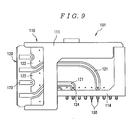
- the connector shown in Figs. 8 and 9 of Patent US 6171115 is known as a conventional connector of this type.
- This connector 101 comprises an insulating housing 110 and a plurality of boards 120 that are supported in a row in the housing 110.
- Each board 120 is constructed from an insulating board material such as FR4, and has a plurality of signal conductor patterns 121 and a plurality of ground conductor patterns 122 that are formed so that the ground conductor patterns surround the signal conductor patterns 121 with a specified distance retained between the respective patterns. These patterns are disposed on the front and back surfaces of each board 120.
- the signal conductor patterns 121 extend from the mating end parts 123 of the boards 120 on the side where a mating connector (not shown in the figures) is mated to the mounting end parts 124 of the boards 120 on the side where a circuit board (not shown in the figures) is connected.
- the ground conductor patterns 122 extend from points located slightly to the inside of the mating end parts 123 of the boards 120 on the side where the mating connector is mated to the mounting end parts 124 of the boards 120 on the side where the circuit board is connected.
- a plurality of contacts 130 that are connected to the signal conductor patterns 121 and the ground conductor patterns 122 are disposed on the mounting end parts 124 of the respective boards 120.
- the housing 110 comprises a front part housing 111 and an accommodating body 114.
- the front part housing 111 comprises a vertical wall 111a that extends in the vertical direction, and a top part 11b that extends rearward (to the left in Fig. 8) from the upper end of the vertical wall 111a.
- the accommodating body 114 comprises a platform part 114a that extends in the forward-rearward direction, and a rear vertical wall part 114b that extends upwardly from the rear end of the platform part 114a.
- the signal conductor patterns 121 formed on the side of the mating end parts 123 of the respective boards 120 are utilized as male type contacts, and are mated and connected with female type contacts (not shown in the figures) disposed on the side of the mating connector. Furthermore, the plurality of contacts 130 disposed on the mounting end parts 124 of the respective boards 120 are connected to the circuit board. As a result, the impedance of the signal paths inside the connector 101 can be maintained at a uniform value, so that data signals can be transmitted at a high speed.
- Fig. 10 of Patent US 6384341 discloses a configuration in which multi-layer boards 301 and 302 are connected to each other by a connector assembly comprising a first connector 101 shown in Figs. 8 and 9 and a second connector 201 that is mated with this first connector 101.
- the signal conductor patterns 121 formed on the side of the mating end parts 123 (see Fig. 9) of the respective boards 120 are utilized as male type contacts, and are mated and connected with female type contacts 202 disposed in the second connector 201. Furthermore, the male type contacts 202 of the second connector 201 are connected to the multi-layer board 301. Moreover, the plurality of contacts 130 disposed on the mounting end parts 124 (see Fig. 9) of the respective boards 120 are connected to the multi-layer board 302. As a result, the impedance of the signal paths inside the connector assembly comprising the first connector 101 and second connector 201 can be maintained at a uniform value, so that data signals can be transmitted at a high speed.
- Fig. 11 of laid-open Japanese patent application H5-21119 discloses a connector 401 in which a plurality of female type contacts 425 are connected to the respective end parts of a plurality of lead film boards 421, 422, 423 and 424, and these female type contacts 425 are secured inside a housing 410.
- a plurality of signal conductor patterns 421a and ground conductor patterns 421b are formed on the surfaces of the respective lead film boards 421, 422, 423 and 424, and the female type contacts 425 are connected by soldering connections to one end part of each of the conductor patterns 421a and 421b.
- contacts 426 that are connected to a circuit board PCB are disposed on the other end parts of the respective conductor patterns 421a and 421b.
- the symbol 421c indicates shielding patterns for preventing crosstalk.
- the female type contacts 202 disposed inside the second connector 201 have a structure in which these contacts make receiving contact or elastic contact with the signal conductor patterns 121 (formed on the respective boards 120) used as male type contacts during mating with these male type contacts, these female type contacts are susceptible to damage at the time of mating with the male type contacts. Consequently, as insertion and extraction of the first connector 101 and second connector 201 are repeated, there is a high probability that damaged female type contacts 202 will be generated. Accordingly, it is desirable that it be easy to replace damaged female type contacts 202.
- the present invention was devised in the light of the problems described above. It is an object of the present invention to provide a connector assembly which allows the easy replacement of easily damaged female type contacts, and which can be used in data transfer systems such as communications devices that transmit data signals at a high speed.
- the connector assembly according to Claim 1 comprises a first connector having a plurality of first boards which have conductor patterns formed on the surfaces thereof, a second connector having a plurality of second boards which have conductor patterns formed on the surfaces thereof, and a relay connector which is attached to the first connector or second connector, and in which a plurality of female type contacts having first female type contact parts that contact the conductor patterns of the first boards and second female type contact parts that contact the conductor patterns of the second boards are press-fitted.
- female type contact part includes both cases in which the conductor patterns on the board surfaces are contacted with the end parts of the first board received, and cases in which the conductor patterns on the board surfaces are elastically contacted without receiving the end parts the first board.
- the first connector is mounted on a motherboard, and a plurality of electrical wires are connected by soldering to the second boards of the second connector.
- the connector assembly is constructed from a first connector A, a second connector B, and a relay connector C.
- the first connector A comprises an insulating housing 10 and a plurality of first boards 26 that are supported in a row in the housing 10.
- the respective first boards 26 have the same function as the boards 120 shown in Fig. 8; each of these boards has a mounting part 27 for mounting on a motherboard (not shown in the figures), which extends in the forward-rearward direction (the left-right direction in Fig. 1), and a mating part 28 for mating with the relay connector C, which extends downward from the mounting part 27, and each board 26 is formed substantially in an L shape.
- Each first board 26 is constructed from an insulating board material such as FR4, and a plurality of signal conductor patterns (not shown in the figures) and a plurality of ground conductor patterns (not shown in the figures) which are formed so that these ground conductor patterns surround the signal conductor patterns with a specified distance retained between the two types of patterns are formed on the front and back surfaces of each first board 26.
- the signal conductor patterns are terminated by conductive pads 30 that are disposed on the front end parts of these mating parts 28, while in the mounting parts 27, these signal conductor patterns are terminated by conductive pads 29 disposed on the lower end parts of the mounting parts 27.
- the ground conductor patterns are terminated by conductive pads 29 disposed on the lower end parts of the mounting parts 27.
- the housing 10 comprises a front part housing 11 and an accommodating body 17.
- the front part housing 11 comprises a mating part 12 that extends in the vertical direction, and a top part 13 that extends rearward from the upper end of the mating part 12.
- This front part housing 11 is formed by molding an insulating resin.
- a plurality of slits 14 through which the mating parts 28 of the respective first board parts 26 are passed are formed in the mating part 12.
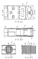
- the respective slits 14 extend in the vertical direction of the mating part 12, and pass through the mating part 12 in the forward-rearward direction as shown in Fig. 3 (B). As is shown in Fig.
- the accommodating body 17 comprises a platform part 18 that extends in the forward-rearward direction, and a rear vertical wall part 19 that extends upward from the rear end of the platform part 18.
- This accommodating body 17 is formed by molding an insulating resin.
- a plurality of grooves 20 into which the lower end parts of the mounting parts 27 of the respective first boards 26 are inserted are formed in the platform part 18.
- a plurality of contact disposition holes 20a for the disposition of the contacts 22 that contact the conductive pads 29 of the first boards 26 are formed in the bottom parts of the respective grooves 20.
- a plurality of grooves 21 into which the rear end parts of the mounting parts 27 of the respective first boards 26 are inserted are formed in the rear vertical wall part 19.
- the front part housing 11 and accommodating body 17 are locked to each other by locking means not shown in the figures.
- each of the contacts 22 comprises a base part 23 which is disposed inside the corresponding contact disposition hole 20a of the accommodating body 17, a pair of elastic contact arms 25 that extend upward from the upper end of the base part 23 via shoulder parts 24, and a press-fitting part 26 which extends downward from the base part 23.
- These contacts 22 are formed by stamping metal plates.
- the contacts 22 are devised so that when the base parts 23 are disposed inside the contact disposition holes 20a, the shoulder parts 24 are positioned on the bottom parts of the slits 20, so that downward movement is restricted.
- the pair of elastic contact arms 25 receive and contact the conductive pads 29 of the first boards 26, and the press-fitting parts 26 are press-fitted in the motherboard when the first connector A is mounted on the motherboard.
- the second connector B comprises a metal housing 60 and a plurality of second boards 64 that are attached in a row inside the housing 60.
- the housing 60 comprises a mating part 61 which has a recess that receives the second connector mating part 42 of the relay connector C, and a cable lead-out part 62 which is disposed on the end part on the opposite side from the mating part 61.
- Latch arms 63 are formed on the mating part 61.
- the respective second boards 64 are constructed from an insulating board material such as FR4, and a plurality of signal conductor patterns (not shown in the figures) and a plurality of ground conductor patterns (not shown in the figures) are formed on the front and back surfaces of each second board 64.
- the signal conductor patterns are terminated by conductive pads 65 disposed on these mating-side end parts, while on the opposite sides, the signal conductor patterns are terminated by conductive pads 66 disposed on substantially the central portions of the second boards 64.
- Each of the second boards 64 is attached to the housing 60 so that the end part on the side of mating with the relay connector C protrudes into the recess of the mating part 61 of the housing 60.
- the core wire 72 of an insulated electrical wire 71 is connected by soldering to each of the conductive pads 66 of each second board 64. Furthermore, a plurality of cables 70 each bundling a plurality of insulated electrical wires 71 are led out to the outside via the cable lead-out part 62.
- the relay connector C comprises an insulating housing 40 and a plurality of rows of female type contacts 50 that are press-fitted in the housing 40.
- the housing 40 comprises a first connector mating part 41 which has a recess that receives the mating part 12 of the first connector A, and a second connector mating part 42 that protrudes forward (to the left in Fig. 1) from the first connector mating part 41.
- the housing 40 is formed by molding an insulating resin.
- locking holes 45 in which the locking projections 16 formed on the mating part 12 of the first connector A are locked by insertion are formed in the upper end surface of the first connector mating part 41.
- a plurality of slits 43 which receive the mating-side end parts of the second boards 64 of the second connector B are formed in the second connector mating part 42.
- Each of the slits 43 extends in the vertical direction of the second connector mating part 42 as shown in Figs. 1 through 3. Furthermore, a latch arm anchoring hole 46 in which one of the latch arms 63 of the second connector B is anchored is formed in the top of the second connector mating part 42.
- each female type contact 50 comprises a press-fitting base part 51 which is press-fitted in the bottom wall of the recess of the first connector mating part 41 of the housing 40, a pair of first elastic contact arms (first female type contact part) 52 which extend from the press-fitting base part 51 into the interior of the recess of the first connector mating part 41, and a pair of second elastic contact arms (second female type contact part) 53 which extend from the press-fitting base part 51 into the interior of a second female type contact part accommodating recess 47 formed in the corresponding slit 43 of the second connector mating part 42.
- Each female type contact 50 is formed by stamping and forming a metal plate.
- a plurality of barbs 51a which are anchored by press-fitting in the lower wall of the recess of the first connector mating part 41 are formed in the upper and lower edges of the press-fitting base part 51.
- the first elastic contact arms 52 are arranged so that these arms elastically contact the conductive pads 30 in which the signal conductor patterns of the first boards 26 are terminated when the relay connector C is mated with the first connector A.
- the second elastic contact arms 53 are arranged so that these arms elastically contact the conductive pads 65 in which the signal conductor patterns of the second boards 64 are terminated when the second connector B is mated with the relay connector C.
- the relay connector C is mated with the first connector A and attached to the first connector A before the second connector B is mated.
- the mating part 12 of the first connector A is inserted into the recess of the first connector mating part 41 of the relay connector C, and the locking projections 16 of the first connector A are locked in the locking holes 45 of the relay connector C.
- the first elastic contact arms 52 of the female type contacts 50 of the relay connector C elastically contact the conductive pads 30 of the first boards 26, so that the female type contacts 50 are electrically continuous with the contacts 22 and motherboard via the signal conductor patterns on the first boards 26.
- the second connector B is mated with the relay connector C after the relay connector C has been attached to the first connector A.
- the connector assembly is completed.
- the second connector mating part 42 of the relay connector C is inserted into the recess of the mating part 61 of the second connector B, and the latch arms 63 of the second connector B are anchored in the latch arm anchoring holes 46 of the relay connector C.
- the conductive pads 65 of the second boards 64 of the second connector B contact the second elastic contact arms 53 of the female type contacts 50 of the relay connector C.
- the insulated electrical wires 71 are electrically continuous with the female type contacts 50 of the relay connector C via the signal conductor patterns on the second boards 64, and are further electrically continuous with the contacts 22 and motherboard via the signal conductor patterns on the first boards 26 of the first connector A.
- the conductive pads 30 in which the signal conductor patterns of the respective first boards 26 are terminated and the conductive pads 65 in which the signal conductor patterns of the respective second boards 64 are terminated are utilized as male type contacts, and these male type contacts contact the female type contacts 50 of the relay connector C. Furthermore, the conductive pads 29 in which the signal conductor patterns of the respective first boards 26 are terminated are connected to the motherboard via the contacts 22, while the insulated electrical wires 71 are connected by soldering to the conductive pads 66 in which the signal conductor patterns of the respective second boards 64 are terminated. As a result, the impedance of the signal paths inside the connector assembly can be maintained at a uniform value, so that data signals can be transmitted at a high speed.
- the second connector B is mated with the relay connector C in a state in which the relay connector C has already been attached to the first connector A; accordingly, the second elastic contact arms 53 of the female type contacts 50 (disposed in the relay connector C) that are contacted by the conductive pads 65 of the second connector B are easily damaged.
- the corresponding female type contacts 50 are replaced by the following method.
- the relay connector C is removed from the first connector A. Then, the corresponding female type contact 50 is removed from the housing 40, and a new female type contact 50 is press-fitted into the housing 40. Then, it is necessary merely to mate the relay connector C with the first connector A, and then to mate the second connector B with the relay connector C. Accordingly, in the connector assembly of the present embodiment, there is no need to remove the relay connector C from the motherboard, etc., when female type contacts 50 are replaced, and damaged female contacts 50 can be replaced by the simple method described above.
- the connector assembly is arranged so that the relay connector C is first attached to the first connector A; however, it would also be possible to attach the relay connector C to the second connector B, and to mate the first connector A with the relay connector C.
- first female type contact parts and second female type contact parts of the female type contacts 50 are respectively constructed from elastic contact arms 52 that elastically contact the conductive pads 30 formed on the surfaces of the first boards 26 and elastic contact arms 53 that elastically contact the conductive pads 65 formed on the surfaces of the second boards 64; however, it would also be possible to devise these contact parts so that the parts receive the end parts of the first boards 26 or second boards 64 and contact the conductive pads 30 or 65 on the surfaces of the boards.
- the connector assembly comprises a first connector having a plurality of first boards which have conductor patterns formed on the surfaces thereof, a second connector having a plurality of second boards which have conductor patterns formed on the surfaces thereof, and a relay connector which is attached to the first connector or second connector, and in which a plurality of female type contacts having first female type contact parts that contact the conductor patterns of the first boards and second female type contact parts that contact the conductor patterns of the second boards are press-fitted. Accordingly, the replacement of the easily damaged female type contacts can easily be accomplished.
- the connector assembly according to Claim 2 is the invention according to Claim 1, wherein the first connector is mounted on a motherboard, and a plurality of electrical wires are connected by soldering to the second boards of the second connector. Accordingly, electrical connections between the motherboard and the electrical wires can easily be established.
- contacts 50 are described as being female type contacts the contact arms of each contact may rest against contact pad(s) on one side only of a respective board.
Landscapes
- Engineering & Computer Science (AREA)
- Architecture (AREA)
- Civil Engineering (AREA)
- Structural Engineering (AREA)
- Chemical & Material Sciences (AREA)
- Analytical Chemistry (AREA)
- Physics & Mathematics (AREA)
- General Physics & Mathematics (AREA)
- Coupling Device And Connection With Printed Circuit (AREA)
- Details Of Connecting Devices For Male And Female Coupling (AREA)
- Connector Housings Or Holding Contact Members (AREA)
Applications Claiming Priority (2)
| Application Number | Priority Date | Filing Date | Title |
|---|---|---|---|
| JP2003145181 | 2003-05-22 | ||
| JP2003145181A JP3964353B2 (ja) | 2003-05-22 | 2003-05-22 | コネクタ組立体 |
Publications (2)
| Publication Number | Publication Date |
|---|---|
| EP1480292A2 true EP1480292A2 (fr) | 2004-11-24 |
| EP1480292A3 EP1480292A3 (fr) | 2006-08-02 |
Family
ID=33095465
Family Applications (1)
| Application Number | Title | Priority Date | Filing Date |
|---|---|---|---|
| EP04252382A Withdrawn EP1480292A3 (fr) | 2003-05-22 | 2004-04-23 | Assemblage connecteur |
Country Status (6)
| Country | Link |
|---|---|
| US (1) | US7044793B2 (fr) |
| EP (1) | EP1480292A3 (fr) |
| JP (1) | JP3964353B2 (fr) |
| KR (1) | KR100851712B1 (fr) |
| CN (1) | CN100401595C (fr) |
| TW (1) | TW200507381A (fr) |
Families Citing this family (47)
| Publication number | Priority date | Publication date | Assignee | Title |
|---|---|---|---|---|
| US20090291593A1 (en) | 2005-06-30 | 2009-11-26 | Prescott Atkinson | High frequency broadside-coupled electrical connector |
| US7163421B1 (en) * | 2005-06-30 | 2007-01-16 | Amphenol Corporation | High speed high density electrical connector |
| US20070141871A1 (en) * | 2005-12-19 | 2007-06-21 | 3M Innovative Properties Company | Boardmount header to cable connector assembly |
| US7553187B2 (en) * | 2006-01-31 | 2009-06-30 | 3M Innovative Properties Company | Electrical connector assembly |
| US7731528B2 (en) | 2006-01-31 | 2010-06-08 | 3M Innovative Properties Company | Electrical termination device |
| CN101517833B (zh) * | 2006-09-14 | 2011-06-22 | 3M创新有限公司 | 电气连接器组件 |
| WO2008124101A2 (fr) * | 2007-04-04 | 2008-10-16 | Amphenol Corporation | Grille de connexion de connecteur électrique |
| US7722401B2 (en) | 2007-04-04 | 2010-05-25 | Amphenol Corporation | Differential electrical connector with skew control |
| US7581990B2 (en) * | 2007-04-04 | 2009-09-01 | Amphenol Corporation | High speed, high density electrical connector with selective positioning of lossy regions |
| US7794240B2 (en) * | 2007-04-04 | 2010-09-14 | Amphenol Corporation | Electrical connector with complementary conductive elements |
| JP5019174B2 (ja) * | 2007-08-03 | 2012-09-05 | 山一電機株式会社 | 高速伝送用コネクタ |
| JP4862796B2 (ja) * | 2007-09-28 | 2012-01-25 | 山一電機株式会社 | 高速伝送用高密度コネクタ |
| EP2240980A2 (fr) | 2008-01-17 | 2010-10-20 | Amphenol Corporation | Ensemble connecteur électrique |
| JP4565031B2 (ja) * | 2008-09-17 | 2010-10-20 | 山一電機株式会社 | 高速伝送用コネクタ、高速伝送コネクタ用プラグ、および、高速伝送コネクタ用ソケット |
| US8172614B2 (en) | 2009-02-04 | 2012-05-08 | Amphenol Corporation | Differential electrical connector with improved skew control |
| JP2010272318A (ja) * | 2009-05-20 | 2010-12-02 | Fujitsu Component Ltd | コネクタ |
| US8550861B2 (en) | 2009-09-09 | 2013-10-08 | Amphenol TCS | Compressive contact for high speed electrical connector |
| CN107069274B (zh) | 2010-05-07 | 2020-08-18 | 安费诺有限公司 | 高性能线缆连接器 |
| WO2012106554A2 (fr) | 2011-02-02 | 2012-08-09 | Amphenol Corporation | Connecteur de type mezzanine |
| JP5640912B2 (ja) * | 2011-07-01 | 2014-12-17 | 山一電機株式会社 | コンタクトユニット、および、それを備えるプリント回路板用コネクタ |
| US9312618B2 (en) | 2011-08-08 | 2016-04-12 | Molex, Llc | Connector with tuned channel |
| WO2014031851A1 (fr) | 2012-08-22 | 2014-02-27 | Amphenol Corporation | Connecteur électrique haute fréquence |
| CN121367083A (zh) | 2014-01-22 | 2026-01-20 | 安费诺有限公司 | 电连接器、子组件、模块、线缆组件、电气组件及电路板 |
| US20160062939A1 (en) * | 2014-08-31 | 2016-03-03 | Airborn, Inc. | Connector with in-circuit programming |
| US10541482B2 (en) | 2015-07-07 | 2020-01-21 | Amphenol Fci Asia Pte. Ltd. | Electrical connector with cavity between terminals |
| CN111755867B (zh) | 2016-08-23 | 2022-09-20 | 安费诺有限公司 | 可配置为高性能的连接器 |
| CN107331995A (zh) * | 2017-03-31 | 2017-11-07 | 安费诺商用电子产品(成都)有限公司 | 小间距高速正交背板连接器 |
| US9997868B1 (en) * | 2017-07-24 | 2018-06-12 | Te Connectivity Corporation | Electrical connector with improved impedance characteristics |
| WO2019084717A1 (fr) | 2017-10-30 | 2019-05-09 | Amphenol Fci Asia Pte Ltd | Connecteur de bord de carte à faible diaphonie |
| JP6981859B2 (ja) | 2017-11-28 | 2021-12-17 | タイコエレクトロニクスジャパン合同会社 | コネクタ |
| CN111727666B (zh) * | 2018-09-04 | 2023-10-27 | 住友电气工业株式会社 | 中继基板、带中继基板的差分传送用电线及带连接器的线缆 |
| CN208862209U (zh) | 2018-09-26 | 2019-05-14 | 安费诺东亚电子科技(深圳)有限公司 | 一种连接器及其应用的pcb板 |
| CN113169484A (zh) | 2018-10-09 | 2021-07-23 | 安费诺商用电子产品(成都)有限公司 | 高密度边缘连接器 |
| US11381015B2 (en) | 2018-12-21 | 2022-07-05 | Amphenol East Asia Ltd. | Robust, miniaturized card edge connector |
| CN111585098B (zh) | 2019-02-19 | 2025-08-19 | 安费诺有限公司 | 高速连接器 |
| TWM582251U (zh) | 2019-04-22 | 2019-08-11 | 香港商安費諾(東亞)有限公司 | Connector set with built-in locking mechanism and socket connector thereof |
| US11799230B2 (en) | 2019-11-06 | 2023-10-24 | Amphenol East Asia Ltd. | High-frequency electrical connector with in interlocking segments |
| US11588277B2 (en) | 2019-11-06 | 2023-02-21 | Amphenol East Asia Ltd. | High-frequency electrical connector with lossy member |
| CN115428275B (zh) | 2020-01-27 | 2025-12-30 | 富加宜(美国)有限责任公司 | 高速连接器 |
| WO2021154718A1 (fr) | 2020-01-27 | 2021-08-05 | Fci Usa Llc | Connecteur orthogonal à accouplement direct à haute densité et à grande vitesse |
| US11652307B2 (en) | 2020-08-20 | 2023-05-16 | Amphenol East Asia Electronic Technology (Shenzhen) Co., Ltd. | High speed connector |
| CN212874843U (zh) | 2020-08-31 | 2021-04-02 | 安费诺商用电子产品(成都)有限公司 | 电连接器 |
| CN215816516U (zh) | 2020-09-22 | 2022-02-11 | 安费诺商用电子产品(成都)有限公司 | 电连接器 |
| CN213636403U (zh) | 2020-09-25 | 2021-07-06 | 安费诺商用电子产品(成都)有限公司 | 电连接器 |
| US11923630B2 (en) * | 2020-11-02 | 2024-03-05 | Fuding Precision Industry (Zhengzhou) Co., Ltd. | Electrical connector assembly including an internal circuit board having three rows of conductive pads respectively at three end portions thereof |
| US12176650B2 (en) | 2021-05-05 | 2024-12-24 | Amphenol East Asia Limited (Hong Kong) | Electrical connector with guiding structure and mating groove and method of connecting electrical connector |
| CN215266741U (zh) | 2021-08-13 | 2021-12-21 | 安费诺商用电子产品(成都)有限公司 | 一种满足高带宽传输的高性能卡类连接器 |
Family Cites Families (12)
| Publication number | Priority date | Publication date | Assignee | Title |
|---|---|---|---|---|
| JPH0521119A (ja) | 1991-07-02 | 1993-01-29 | Augat Inc | 多極コネクタ |
| US6083047A (en) * | 1997-01-16 | 2000-07-04 | Berg Technology, Inc. | Modular electrical PCB assembly connector |
| US5924899A (en) * | 1997-11-19 | 1999-07-20 | Berg Technology, Inc. | Modular connectors |
| US6443740B1 (en) * | 1998-10-15 | 2002-09-03 | Fci Americas Technology, Inc. | Connector system |
| US6171115B1 (en) * | 2000-02-03 | 2001-01-09 | Tyco Electronics Corporation | Electrical connector having circuit boards and keying for different types of circuit boards |
| US6494723B2 (en) * | 2000-03-31 | 2002-12-17 | Autonetworks Technologies, Ltd. | Terminal that provides connection between a wire circuit and a printed circuit, and electric junction box including said terminal |
| JP3489054B2 (ja) * | 2000-10-06 | 2004-01-19 | 日本航空電子工業株式会社 | コネクタ組付け体 |
| JP3491064B2 (ja) * | 2000-10-20 | 2004-01-26 | 日本航空電子工業株式会社 | 高速伝送用コネクタ |
| US6621391B2 (en) * | 2001-04-24 | 2003-09-16 | Agilent Technologies, Inc. | Relay |
| US6540522B2 (en) * | 2001-04-26 | 2003-04-01 | Tyco Electronics Corporation | Electrical connector assembly for orthogonally mating circuit boards |
| US6384341B1 (en) * | 2001-04-30 | 2002-05-07 | Tyco Electronics Corporation | Differential connector footprint for a multi-layer circuit board |
| US6692272B2 (en) * | 2001-11-14 | 2004-02-17 | Fci Americas Technology, Inc. | High speed electrical connector |
-
2003
- 2003-05-22 JP JP2003145181A patent/JP3964353B2/ja not_active Expired - Fee Related
-
2004
- 2004-04-23 EP EP04252382A patent/EP1480292A3/fr not_active Withdrawn
- 2004-04-26 TW TW093111586A patent/TW200507381A/zh unknown
- 2004-05-03 KR KR1020040031076A patent/KR100851712B1/ko not_active Expired - Fee Related
- 2004-05-17 US US10/847,039 patent/US7044793B2/en not_active Expired - Fee Related
- 2004-05-24 CN CNB2004100457437A patent/CN100401595C/zh not_active Expired - Fee Related
Also Published As
| Publication number | Publication date |
|---|---|
| KR20040100895A (ko) | 2004-12-02 |
| TW200507381A (en) | 2005-02-16 |
| JP2004349126A (ja) | 2004-12-09 |
| CN1574508A (zh) | 2005-02-02 |
| US7044793B2 (en) | 2006-05-16 |
| US20040235352A1 (en) | 2004-11-25 |
| JP3964353B2 (ja) | 2007-08-22 |
| KR100851712B1 (ko) | 2008-08-11 |
| CN100401595C (zh) | 2008-07-09 |
| EP1480292A3 (fr) | 2006-08-02 |
Similar Documents
| Publication | Publication Date | Title |
|---|---|---|
| US7044793B2 (en) | Connector assembly | |
| US4867690A (en) | Electrical connector system | |
| CN107871987B (zh) | 电连接器 | |
| US6296496B1 (en) | Electrical connector and method for attaching the same to a printed circuit board | |
| US6478611B1 (en) | Electrical connector with visual indicator | |
| CN101828308B (zh) | 电连接器组件 | |
| US6808419B1 (en) | Electrical connector having enhanced electrical performance | |
| US6623310B1 (en) | High density electrical connector assembly with reduced insertion force | |
| US6343951B1 (en) | Electrical connector | |
| US6811434B2 (en) | Stacked electrical connector | |
| CN100372180C (zh) | 改进的插座 | |
| US8353728B2 (en) | Receptacle connector having contact modules and plug connector having a paddle board | |
| US20120156938A1 (en) | Plug connector with improved circuit card to lower cross-talking therein | |
| US6592407B2 (en) | High-speed card edge connector | |
| US7445497B2 (en) | Electrical connector | |
| WO2010096567A1 (fr) | Connecteur vertical pour carte de circuit imprimé | |
| US20100151743A1 (en) | Electrical adapter | |
| CN102509956B (zh) | 收发器组件 | |
| US6918775B2 (en) | Method for interconnecting multiple printed circuit boards | |
| US20080026608A1 (en) | Connector for Printed Circuit Boards Stacked One On Another | |
| CN101208835A (zh) | 电互连系统 | |
| US7351091B1 (en) | Header connector | |
| US6645009B1 (en) | High density electrical connector with lead-in device | |
| CN102709755B (zh) | 收发器组件 | |
| CN100502154C (zh) | 带有电线管理系统的电气连接器 |
Legal Events
| Date | Code | Title | Description |
|---|---|---|---|
| PUAI | Public reference made under article 153(3) epc to a published international application that has entered the european phase |
Free format text: ORIGINAL CODE: 0009012 |
|
| AK | Designated contracting states |
Kind code of ref document: A2 Designated state(s): AT BE BG CH CY CZ DE DK EE ES FI FR GB GR HU IE IT LI LU MC NL PL PT RO SE SI SK TR |
|
| AX | Request for extension of the european patent |
Extension state: AL HR LT LV MK |
|
| PUAL | Search report despatched |
Free format text: ORIGINAL CODE: 0009013 |
|
| AK | Designated contracting states |
Kind code of ref document: A3 Designated state(s): AT BE BG CH CY CZ DE DK EE ES FI FR GB GR HU IE IT LI LU MC NL PL PT RO SE SI SK TR |
|
| AX | Request for extension of the european patent |
Extension state: AL HR LT LV MK |
|
| 17P | Request for examination filed |
Effective date: 20070124 |
|
| AKX | Designation fees paid |
Designated state(s): DE FR GB IT NL |
|
| 17Q | First examination report despatched |
Effective date: 20091026 |
|
| STAA | Information on the status of an ep patent application or granted ep patent |
Free format text: STATUS: THE APPLICATION IS DEEMED TO BE WITHDRAWN |
|
| 18D | Application deemed to be withdrawn |
Effective date: 20100306 |