EP1480334B1 - Procédé et dispositif pour agrandir la taille d'un transistor au-dela d'un circuit intégré - Google Patents
Procédé et dispositif pour agrandir la taille d'un transistor au-dela d'un circuit intégré Download PDFInfo
- Publication number
- EP1480334B1 EP1480334B1 EP04252802A EP04252802A EP1480334B1 EP 1480334 B1 EP1480334 B1 EP 1480334B1 EP 04252802 A EP04252802 A EP 04252802A EP 04252802 A EP04252802 A EP 04252802A EP 1480334 B1 EP1480334 B1 EP 1480334B1
- Authority
- EP
- European Patent Office
- Prior art keywords
- master
- slave
- circuit
- integrated circuit
- coupled
- Prior art date
- Legal status (The legal status is an assumption and is not a legal conclusion. Google has not performed a legal analysis and makes no representation as to the accuracy of the status listed.)
- Expired - Lifetime
Links
Images

Classifications
-
- H—ELECTRICITY
- H03—ELECTRONIC CIRCUITRY
- H03K—PULSE TECHNIQUE
- H03K17/00—Electronic switching or gating, i.e. not by contact-making and –breaking
- H03K17/51—Electronic switching or gating, i.e. not by contact-making and –breaking characterised by the components used
- H03K17/56—Electronic switching or gating, i.e. not by contact-making and –breaking characterised by the components used by the use, as active elements, of semiconductor devices
- H03K17/687—Electronic switching or gating, i.e. not by contact-making and –breaking characterised by the components used by the use, as active elements, of semiconductor devices the devices being field-effect transistors
- H03K17/6871—Electronic switching or gating, i.e. not by contact-making and –breaking characterised by the components used by the use, as active elements, of semiconductor devices the devices being field-effect transistors the output circuit comprising more than one controlled field-effect transistor
- H03K17/6874—Electronic switching or gating, i.e. not by contact-making and –breaking characterised by the components used by the use, as active elements, of semiconductor devices the devices being field-effect transistors the output circuit comprising more than one controlled field-effect transistor in a symmetrical configuration
-
- H—ELECTRICITY
- H03—ELECTRONIC CIRCUITRY
- H03F—AMPLIFIERS
- H03F3/00—Amplifiers with only discharge tubes or only semiconductor devices as amplifying elements
- H03F3/20—Power amplifiers, e.g. Class B amplifiers, Class C amplifiers
- H03F3/21—Power amplifiers, e.g. Class B amplifiers, Class C amplifiers with semiconductor devices only
- H03F3/217—Class D power amplifiers; Switching amplifiers
-
- H—ELECTRICITY
- H03—ELECTRONIC CIRCUITRY
- H03K—PULSE TECHNIQUE
- H03K17/00—Electronic switching or gating, i.e. not by contact-making and –breaking
- H03K17/12—Modifications for increasing the maximum permissible switched current
- H03K17/122—Modifications for increasing the maximum permissible switched current in field-effect transistor switches
Definitions
- the present invention relates generally to integrated circuits and, more specifically, the present invention relates to integrated circuits that include power transistors.
- Electronic circuits using power transistors have to be designed according to the rating or size of the power transistors being used.
- the size of the power transistors being used influences their power handling capability, which is specified by the power transistor manufacturers. Since the packages used to house power transistors are limited in size by physical and economic constraints, the size of the power transistors that can be contained in a single package is similarly limited. To effectively extend the size of power transistors where necessary, it is therefore common to design electronic circuits using power transistors with two or more power transistors coupled together.
- the resulting combination of power transistors is typically controlled with a single control circuit consisting of control circuitry and a single driver circuit to drive the power transistors. Circuits using two or more power transistors coupled in this way require careful use of driver and control circuits, in addition to careful circuit board layout, appropriate to the characteristics of the type of power transistor being used.
- Integrated circuits are available that integrate control circuitry, drivers and power transistors.
- the size of the power transistors used in these integrated circuits is also limited by the packages used to house the integrated circuits. In this case, coupling of additional external power transistors is usually not possible since the integrated power transistor driver circuitry is typically dedicated to the integrated power transistor and no means is provided for the user to access the necessary driver circuitry outputs.
- the size and number of external power transistors that can be driven by the integrated driver circuitry is limited by the size of this integrated power transistor driver circuitry.
- an apparatus includes a first power transistor on a first integrated circuit chip.
- the first power transistor has two output terminals and a control terminal.
- the apparatus also includes a first driver circuit on the first integrated circuit chip.
- the first driver circuit has a first driver circuit input and a first driver circuit output.
- the first driver circuit output is coupled to drive the control terminal of the first power transistor.
- the apparatus further includes a second power transistor on a second integrated circuit chip.
- the second power transistor has two output terminals and a control terminal.
- the apparatus also includes a second driver circuit on the second integrated circuit chip.
- the second driver circuit has a second driver circuit input and a second driver circuit output.
- the second driver circuit output is coupled to drive the control terminal of the second power transistor.
- the two output terminals of the first power transistor are coupled to the two output terminals, respectively, of the second power transistor.
- the first and second driver circuit inputs all coupled to be driven by a single control signal output by a master control circuit on the first integrated circuit chip. Additional features and benefits of the present invention will become apparent from the detailed description and figures set forth below.
- Figure 1 is a schematic illustrating a circuit where the size of the power transistor has been extended by coupling two power transistors to be driven by a single power transistor driver circuit.
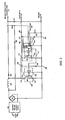
- Figure 2 is a schematic illustrating one embodiment of a circuit wherein the size of the power transistor has been extended by coupling a plurality of integrated circuits in accordance with the teachings of the present invention.
- Figure 3 is a schematic illustrating another embodiment of a circuit wherein the size of the power transistor has been extended by coupling a plurality of integrated circuits in accordance with the teachings of the present invention.
- a simple and novel technique for extending the size of a power transistor is provided according to embodiments of the present invention by coupling together two or more integrated circuits chips, each of which includes at least a power transistor and power transistor driver circuitry.
- a control circuit is part of one of the integrated circuits and includes an output that is a control signal.
- the control signal is coupled to be an input to the power transistor driver circuitry of the two or more integrated circuits that are coupled together.
- the power transistor driver circuitry is extended as appropriate to the extension of the power transistor in accordance with the teachings of the present invention.
- Figure 1 shows a schematic of a circuit where two power transistors 100 and 101 are coupled together with a common connection to a load 115. Since power transistors 100 and 101 are not part of any integrated circuit, they are often described as discrete power transistors. In this way, the effective size of the power transistor is extended. Output terminals, 118 and 121, of power transistors 100 and 101 are coupled together. Output terminals, 119 and 122, of power transistors 100 and 101 are coupled together. Control terminals 120 and 123 of power transistors 100 and 101, respectively, are coupled together through resistors 102 and 103. Resistors 102 and 103 are in turn coupled together to driver circuit output 109 of driver circuit 104.
- driver circuit 104 is part of an integrated circuit 106 having a power source terminal 111, a ground terminal 110 and coupled to receive an input signal 114 at terminal 124.
- the integrated circuit 106 further includes a control circuit 105.
- Control circuit 105 can for example be a pulse width modulator (PWM) controller in a power conversion circuit or any other suitable controller applied to control power transistors in an electronic circuit.
- PWM pulse width modulator
- the drive capabilities of the drive circuit 104 limits the number of discrete power transistors that can be configured as shown in Figure 1 .
- Each discrete power transistor control terminal requires electrical energy to be driven according to the requirements and the maximum capability of driver circuit 104 to deliver this electrical energy limits the number of discrete power transistors that can be connected to extend the power transistor size.
- FIG. 2 shows generally one embodiment of a circuit in accordance with the teachings of the present invention.
- integrated circuit chip 209 includes a power transistor 201, a driver circuit 203 and a control circuit 204.
- Integrated circuit chip 208 includes a power transistor 200 and a driver circuit 202.
- the output terminals 214 and 215 of power transistor 201 are coupled to the output terminals 210 and 211 respectively of power transistor 200 as shown.
- the control signal output 229, of control circuit 204 is coupled to the inputs of driver circuits 203 and 202 as shown.
- the output of driver circuit 203 is coupled to the control terminal 223 of power transistor 201 and the output of driver circuit 202 is coupled to the control terminal 222 of power transistor 200.
- power transistors 200 and 201 may be implemented with field effect transistors (FETs), metal oxide field effect transistors (MOSFETs), bipolar transistors or other suitable types of devices.
- FETs field effect transistors
- MOSFETs metal oxide field effect transistors
- the power source terminals 213 and 216 of integrated circuits 208 and 209 respectively are coupled to a single power source 221.
- the fact that the driver circuit 203 and power transistor 201 are both part of integrated circuit chip 209 allows the power source for integrated circuit chip 208 to be decoupled by capacitor 206 close to the integrated circuit chip 209.
- the fact that the driver 202 and power transistor 200 are both part of integrated circuit chip 208 allows the power source for integrated circuit chip 208 to be decoupled with capacitor 205 close to integrated circuit chip 208.
- decoupling capacitors 205 and 206 can be located close to their respective integrated circuit chips 208 and 209 reduces the parasitic effects when driving the respective power transistors 200 and 201, discussed above with relation to Figure 1 .
- the physical separation between integrated circuit chips 208 and 209 is therefore much less important than the physical separation between integrated circuit 106 and power transistors 100 and 101 in the circuit of Figure 1 , since the control signal coupled through connection 217 is typically a low power digital signal and therefore less prone to the parasitic effects of the higher power driver circuit output signal 109 in Figure 1 .
- the integration of power transistor and driver circuits according to embodiments of the present invention means that the driver circuit size is extended in proportion to the extension of the power transistor. It is therefore possible to couple many more power transistors according to embodiments of the present invention than was previously possible with discrete power transistors being driven with a single drive circuit 104 as shown on Figure 1 .
- the embodiment depicted in Figure 2 can also be considered as including a master integrated circuit chip 209, having a master semiconductor switch 201 and master driver circuit 203 and a slave integrated circuit chip 208 having a slave semiconductor switch 200 and a slave driver circuit 202.
- the master slave description helps illustrate the fact that master integrated circuit chip 209 can be designed to integrate many or all control and protection functions necessary in the circuit 230.
- master control circuit 204 includes a current sense circuit 231 which is used to sense the current flowing in master semiconductor switch 201 between master switch terminals, 214 and 215.
- the master semiconductor switch is a metal oxide field effect transistor (MOSFET)
- the current may be sensed for example by master control circuit 204 current sense circuit 231 by sensing the voltage drop across the on-resistance of the master semiconductor switch 201 when it is on.
- the MOSFET is normally switched off.
- Current sensed in the main semiconductor switch 201 can be used to control current flowing in the slave semiconductor switch 200, since the current flowing in master semiconductor switch 201 is representative of the current flowing in slave semiconductor switch 200 when both switches are on.
- master control circuit 204 includes a temperature sense circuit 232 thermally coupled to sense the temperature master semiconductor switch 201. If master control circuit 204 temperature sense circuit 232 determines that the temperature of master semiconductor switch 201 is too high, the master control signal 229 will cause both master and slave semiconductor switches 200 and 201 to turn off to control the power dissipation in both semiconductor switches 200 and 201.
- FIG 3 shows generally another embodiment of a circuit in accordance with the teachings of the present invention.
- the circuit elements shown in Figure 2 are shown in Figure 3 in a boost converter circuit.
- the general configuration of the converter with input alternating current (AC) source 308, rectifier circuit 301, boost inductor 302, boost diode 303 and output bulk capacitor 307 will be familiar to one skilled in the art.
- the circuit is configured as a power factor correction (PFC) controller to perform a PFC function, the requirements of which will again be familiar to one skilled in the art.
- PFC power factor correction
- the input signal 220 to master integrated circuit chip 209 is derived from a combination of current flowing through resistors 304 and 305, which provide the control signal required by master control circuit 204 to perform the PFC function.
- the direct current (DC) output voltage 306 is generally used to provide the input for a subsequent power conversion stage as shown. This power conversion stage could for example be a switched mode power supply.
- power source 221 is derived from the power conversion stage or from a separate auxiliary power supply.
- master control circuit 204 may be implemented in accordance with the teachings of the present invention may also be implemented in other designs including but not limited to switched mode regulators, alternating current (AC) to direct current (DC) power supplies, power amplifiers, motor control circuits, analog and digital audio amplifiers or other suitable types of circuits.
- switched mode regulators alternating current (AC) to direct current (DC) power supplies
- power amplifiers motor control circuits
- analog and digital audio amplifiers or other suitable types of circuits.
- one other terminal 310 of the master control circuit 204 is coupled to a resistor 309, which is further coupled to return 219 or ground.
- master control circuit includes a current limit adjustment circuit 233 coupled to terminal 310 to control or adjust the current limit threshold of master control circuit 204.
- This current limit adjustment circuit 233 need only be included in the master control circuit 204 of the master integrated circuit chip 209 since the master control signal 229 is applied to both master and slave driver circuits 203 and 204 respectively.
Landscapes
- Engineering & Computer Science (AREA)
- Power Engineering (AREA)
- Dc-Dc Converters (AREA)
- Electronic Switches (AREA)
- Rectifiers (AREA)
- Power Conversion In General (AREA)
- Semiconductor Integrated Circuits (AREA)
Claims (21)
- Appareil, comprenant :une puce à circuits intégrés maître (209) incluant un commutateur semi-conducteur maître (201) ayant deux bornes de commutateur maître (214, 215) la puce à circuits intégrés maître (209) incluant en outre un circuit pilote maître (203) ayant une sortie pilote maître et une entrée pilote maître, la sortie pilote maître étant couplée pour piloter la borne de commande maître du commutateur à semi-conducteur maître (201) ; etau moins une puce à circuits intégrés esclave (208) incluant un commutateur à semi-conducteur esclave (200) ayant deux bornes de commutateur esclave et une borne de commande esclave, ladite au moins une puce à circuits intégrés esclave (208) incluant en outre un circuit pilote esclave (202) ayant une sortie pilote esclave et une entrée pilote esclave, la sortie pilote esclave étant couplée pour piloter les bornes de commande esclave du commutateur à semi-conducteur esclave (200),caractérisé en ce que :la puce à circuits intégrés maître (209) inclut une borne de commande maître et un circuit de commande maître (204) couplé pour délivrer un signal de commande maître,les deux bornes de commutateur maître (214, 215) de la puce à circuits intégrés maître (209) sont couplées aux deux bornes de commutateur esclave de ladite au moins une puce à circuits intégrés esclave (208), etl'entrée pilote maître de la puce à circuits intégrés maître (209) et l'entrée pilote esclave de ladite au moins une puce à circuits intégrés esclave (208) sont couplées pour être pilotées par le signal de commande maître.
- Appareil selon la revendication 1, dans lequel le circuit pilote maître et le circuit pilote esclave (203, 202) sont tous couplés pour être alimentés par une source de puissance unique.
- Appareil selon la revendication 1 ou 2, dans lequel le commutateur à semi-conducteur maître et le commutateur à semi-conducteur esclave (201, 200) comprennent des transistors à effet de champ (FET).
- Appareil selon la revendication 3, dans lequel le commutateur à semi-conducteur maître et le commutateur à semi-conducteur esclave (201, 200) comprennent des transistors à effet de champ à semi-conducteur métal/oxyde (MOSFET).
- Appareil selon la revendication 1, 2, 3 ou 4, dans lequel le circuit de commande maître (204) comprend un circuit détecteur de courant (231) couplé au commutateur à semi-conducteur maître pour détecter un courant à travers le commutateur à semi-conducteur maître.
- Appareil selon la revendication 5, dans lequel le circuit de détection de courant (231) est couplé pour amener le circuit de commande maître (204) à couper le commutateur à semi-conducteur maître et le commutateur à semi-conducteur esclave (201, 200) avec le signal de commande maître quand le courant à travers le commutateur à semi-conducteur maître excède un seuil limite de courant.
- Appareil selon la revendication 5, dans lequel le circuit de courant est couplé aux deux bornes de commutateur maître (214, 215).
- Appareil selon la revendication 5, dans lequel le circuit de détection de courant (231) est couplé pour détecter une chute de tension aux bornes d'une résistance branchée sur le commutateur à semi-conducteur maître.
- Appareil selon la revendication 1, dans lequel le circuit de commande maître (204) comprend un circuit de détection de température couplé thermiquement au commutateur à semi-conducteur maître pour détecter une température du commutateur à semi-conducteur maître, le circuit de détection de température étant couplé pour amener le circuit de commande maître (204) à commander la dissipation de puissance du commutateur à semi-conducteur maître et du commutateur à semi-conducteur esclave (201, 200) avec le signal de commande maître.
- Appareil selon la revendication 1, dans lequel le circuit de commande maître (204) comprend un circuit régulateur en mode commuté.
- Appareil selon la revendication 1, dans lequel le circuit de commande maître (204) comprend un circuit contrôleur de facteur de puissance.
- Appareil selon la revendication 1, dans lequel le circuit de commande maître (204) comprend un circuit amplificateur numérique.
- Appareil selon l'une quelconque des revendications 1 à 12, dans lequel l'appareil est inclus dans une alimentation de puissance à mode commuté.
- Appareil selon l'une quelconque des revendications 1 à 12, dans lequel l'appareil est inclus dans une alimentation de puissance de courant alternatif (AC) à courant continu (DC).
- Appareil selon l'une quelconque des revendications 1 à 12, dans lequel l'appareil est inclus dans une alimentation de puissance de courant continu (DC) à courant continu DC.
- Appareil selon l'une quelconque des revendications 1 à 12, dans lequel l'appareil est inclus dans un circuit de correction de facteur de puissance.
- Appareil selon l'une quelconque des revendications 1 à 12, dans lequel l'appareil est inclus dans un circuit amplificateur de puissance numérique.
- Procédé comprenant les étapes consistant à :générer un signal de commande avec un circuit de commande maître (204) inclus dans une puce à circuits intégrés maître (209) ;générer un signal pilote maître avec un circuit pilote maître (203) inclus dans la puce à circuits intégrés maître (209) en réponse au signal de commande ;commander un transistor de puissance maître inclus dans la puce à circuits intégrés maître (209) en réponse au signal pilote maître ;générer au moins un signal pilote esclave avec au moins un circuit pilote esclave inclus dans au moins une puce à circuits intégrés esclave (208) en réponse au signal de commande ; etcommander au moins un transistor de puissance esclave inclus dans ladite au moins une puce à circuits intégrés esclave (208) en réponse audit au moins un signal pilote esclave.
- Procédé selon la revendication 18, dans lequel des bornes de sortie correspondantes du transistor de puissance maître et dudit au moins un transistor de puissance esclave sont couplées ensemble.
- Procédé selon la revendication 18 ou 19, comprenant en outre de détecter un courant à travers le transistor de puissance maître, de sorte que le signal de commande a lieu en réponse au courant à travers le transistor de puissance maître.
- Procédé selon la revendication 18, 19 ou 20, comprenant en outre de détecter une température du transistor de puissance maître, de sorte que le signal de commande a lieu en réponse à la température du transistor de puissance maître.
Applications Claiming Priority (2)
| Application Number | Priority Date | Filing Date | Title |
|---|---|---|---|
| US441790 | 1989-11-27 | ||
| US10/441,790 US6882212B2 (en) | 2003-05-16 | 2003-05-16 | Method and apparatus for extending the size of a transistor beyond one integrated circuit |
Publications (3)
| Publication Number | Publication Date |
|---|---|
| EP1480334A2 EP1480334A2 (fr) | 2004-11-24 |
| EP1480334A3 EP1480334A3 (fr) | 2007-08-08 |
| EP1480334B1 true EP1480334B1 (fr) | 2011-06-22 |
Family
ID=33097973
Family Applications (1)
| Application Number | Title | Priority Date | Filing Date |
|---|---|---|---|
| EP04252802A Expired - Lifetime EP1480334B1 (fr) | 2003-05-16 | 2004-05-14 | Procédé et dispositif pour agrandir la taille d'un transistor au-dela d'un circuit intégré |
Country Status (3)
| Country | Link |
|---|---|
| US (3) | US6882212B2 (fr) |
| EP (1) | EP1480334B1 (fr) |
| JP (1) | JP4495517B2 (fr) |
Families Citing this family (13)
| Publication number | Priority date | Publication date | Assignee | Title |
|---|---|---|---|---|
| US6882212B2 (en) * | 2003-05-16 | 2005-04-19 | Power Integrations, Inc. | Method and apparatus for extending the size of a transistor beyond one integrated circuit |
| US7551007B2 (en) * | 2005-02-11 | 2009-06-23 | Fairchild Semiconductor Corporation | Partial switch gate driver |
| DE102005052800A1 (de) * | 2005-11-05 | 2007-08-16 | Semikron Elektronik Gmbh & Co. Kg | Treiberschaltungsanordnung zur Ansteuerung von leistungselektronischen Schaltungen |
| US7760524B2 (en) * | 2007-10-17 | 2010-07-20 | Power Integrations, Inc. | Method and apparatus to reduce the volume required for bulk capacitance in a power supply |
| US9793889B2 (en) | 2011-03-15 | 2017-10-17 | Infineon Technologies Ag | Semiconductor device including a circuit to compensate for parasitic inductance |
| US9148054B2 (en) | 2013-03-14 | 2015-09-29 | Volterra Semiconductor LLC | Voltage regulators with kickback protection |
| CN105164598B (zh) * | 2013-03-15 | 2017-09-12 | 沃尔泰拉半导体公司 | 具有多个晶体管的电压调节器 |
| DE102013113219A1 (de) * | 2013-11-29 | 2015-06-03 | Hella Kgaa Hueck & Co. | Selbstschützender Halbleiterschalter, Sicherungsvorrichtung sowie Verfahren zum Schalten eines elektrischen Stroms |
| CN111656683B (zh) | 2018-01-30 | 2024-03-08 | 电力集成公司 | 具有校准的参考的信号放大器 |
| US11942900B2 (en) | 2021-10-14 | 2024-03-26 | Power Integrations, Inc. | Signal compensation with summed error signals |
| US12405302B2 (en) * | 2022-02-23 | 2025-09-02 | Stmicroelectronics S.R.L. | Integrated circuit with off-state diagnosis for driver channels |
| US12188991B2 (en) | 2022-02-23 | 2025-01-07 | Stmicroelectronics S.R.L. | Device with fault detection and related system and method |
| US11885845B2 (en) | 2022-02-23 | 2024-01-30 | Stmicroelectronics S.R.L. | Integrated circuit with on-state diagnosis for driver channels |
Family Cites Families (33)
| Publication number | Priority date | Publication date | Assignee | Title |
|---|---|---|---|---|
| US5428287A (en) * | 1992-06-16 | 1995-06-27 | Cherry Semiconductor Corporation | Thermally matched current limit circuit |
| JP2837054B2 (ja) * | 1992-09-04 | 1998-12-14 | 三菱電機株式会社 | 絶縁ゲート型半導体装置 |
| JP3243902B2 (ja) * | 1993-09-17 | 2002-01-07 | 株式会社日立製作所 | 半導体装置 |
| US5442218A (en) * | 1993-09-30 | 1995-08-15 | At&T Global Information Solutions Company | CMOS power fet driver including multiple power MOSFET transistors connected in parallel, each carrying an equivalent portion of the total driver current |
| US5461303A (en) * | 1994-01-31 | 1995-10-24 | Power Integrations, Inc. | Power factor correction precompensation circuit |
| DE19534388B4 (de) * | 1994-09-19 | 2009-03-19 | International Rectifier Corp., El Segundo | IGBT-Transistorbauteil |
| US5500616A (en) * | 1995-01-13 | 1996-03-19 | Ixys Corporation | Overvoltage clamp and desaturation detection circuit |
| US5568041A (en) * | 1995-02-09 | 1996-10-22 | Magnetek, Inc. | Low-cost power factor correction circuit and method for electronic ballasts |
| JP3511721B2 (ja) * | 1995-03-15 | 2004-03-29 | ソニー株式会社 | 情報処理方法及び装置 |
| US5845240A (en) * | 1996-07-24 | 1998-12-01 | Fielder; Mark | Selective recall and preservation of continuously recorded data |
| US6085323A (en) * | 1996-04-15 | 2000-07-04 | Kabushiki Kaisha Toshiba | Information processing system having function of securely protecting confidential information |
| US5796278A (en) * | 1996-04-26 | 1998-08-18 | Delco Electronics Corporaiton | Circuitry for controlling load current |
| US5675297A (en) * | 1996-04-29 | 1997-10-07 | Delco Electronics Corporation | Integrated pulse-width modulation circuit with thermal shutdown circuit |
| US5845210A (en) * | 1996-08-15 | 1998-12-01 | Ericsson, Inc. | Method and apparatus for supporting data transmission over analog and digital cellular telephone air interfaces |
| US5947691A (en) * | 1997-10-29 | 1999-09-07 | Comair Rotron, Inc. | Winding supply circuit with current and thermal protective elements |
| DE19855615A1 (de) * | 1997-12-03 | 1999-06-10 | Fuji Electric Co Ltd | Schaltnetzteil |
| JP3773664B2 (ja) * | 1998-09-11 | 2006-05-10 | 三菱電機株式会社 | 駆動制御装置、モジュール、および、複合モジュール |
| US6278678B1 (en) * | 1999-02-12 | 2001-08-21 | Sony Corporation | Editing apparatus, editing method, and recording medium |
| JP3628576B2 (ja) * | 1999-02-14 | 2005-03-16 | 矢崎総業株式会社 | 微少電流検出装置 |
| MY122279A (en) * | 1999-03-03 | 2006-04-29 | Sony Corp | Nonvolatile memory and nonvolatile memory reproducing apparatus |
| US6259292B1 (en) * | 1999-04-21 | 2001-07-10 | James S. Congdon | Three-terminal inverting hysteretic transistor switch |
| US6380644B1 (en) * | 1999-11-26 | 2002-04-30 | Nortel Networks Limited | Switching circuitry providing improved signal performance at high frequencies and method of operation thereof |
| JP4792636B2 (ja) * | 2001-01-11 | 2011-10-12 | 日本テキサス・インスツルメンツ株式会社 | 誘導性負荷駆動回路 |
| US6930473B2 (en) * | 2001-08-23 | 2005-08-16 | Fairchild Semiconductor Corporation | Method and circuit for reducing losses in DC-DC converters |
| EP1360755A2 (fr) * | 2001-02-06 | 2003-11-12 | Koninklijke Philips Electronics N.V. | Convertisseur cc-cc synchrone |
| WO2002063765A2 (fr) * | 2001-02-06 | 2002-08-15 | Koninklijke Philips Electronics N.V. | Tec et circuit de commande integres |
| JP4770064B2 (ja) * | 2001-06-05 | 2011-09-07 | 富士電機株式会社 | Ipm回路 |
| JP3780898B2 (ja) * | 2001-10-16 | 2006-05-31 | 富士電機デバイステクノロジー株式会社 | パワーデバイスの駆動回路 |
| US6531895B1 (en) * | 2002-02-08 | 2003-03-11 | Delphi Technologies, Inc. | Isolated gate drive circuit having a switched input capacitor |
| JP3708897B2 (ja) * | 2002-04-23 | 2005-10-19 | Necエレクトロニクス株式会社 | 出力バッファ回路 |
| US6737894B1 (en) * | 2003-05-01 | 2004-05-18 | International Business Machines Corporation | Method and apparatus for generating impedance matched output signals for an integrated circuit device |
| US6882212B2 (en) * | 2003-05-16 | 2005-04-19 | Power Integrations, Inc. | Method and apparatus for extending the size of a transistor beyond one integrated circuit |
| JP2005045590A (ja) * | 2003-07-23 | 2005-02-17 | Mitsubishi Electric Corp | 半導体装置 |
-
2003
- 2003-05-16 US US10/441,790 patent/US6882212B2/en not_active Expired - Lifetime
-
2004
- 2004-05-14 EP EP04252802A patent/EP1480334B1/fr not_active Expired - Lifetime
- 2004-05-17 JP JP2004146603A patent/JP4495517B2/ja not_active Expired - Fee Related
-
2005
- 2005-03-08 US US11/079,839 patent/US7038524B2/en not_active Expired - Lifetime
-
2006
- 2006-03-21 US US11/385,638 patent/US7352232B2/en not_active Expired - Fee Related
Also Published As
| Publication number | Publication date |
|---|---|
| EP1480334A2 (fr) | 2004-11-24 |
| US7038524B2 (en) | 2006-05-02 |
| EP1480334A3 (fr) | 2007-08-08 |
| US6882212B2 (en) | 2005-04-19 |
| JP2005176586A (ja) | 2005-06-30 |
| US7352232B2 (en) | 2008-04-01 |
| US20050151577A1 (en) | 2005-07-14 |
| JP4495517B2 (ja) | 2010-07-07 |
| US20060158242A1 (en) | 2006-07-20 |
| US20040227561A1 (en) | 2004-11-18 |
Similar Documents
| Publication | Publication Date | Title |
|---|---|---|
| US9166499B2 (en) | Electronic circuit operating based on isolated switching power source | |
| CN101079576B (zh) | 用于提供对电源调节器的开关的系统 | |
| EP1480334B1 (fr) | Procédé et dispositif pour agrandir la taille d'un transistor au-dela d'un circuit intégré | |
| US7777437B2 (en) | Switching control system and motor driving system | |
| US8724352B2 (en) | Power supply apparatus driving circuit, power supply apparatus driving integrated circuit, and power supply apparatus | |
| KR20040091137A (ko) | 3-단자, 저 전압 펄스 폭 변조 컨트롤러 | |
| US6734656B2 (en) | Buck regulator with monolithic N- channel upper FET and pilot current sensing | |
| KR19990007348A (ko) | 디씨-디씨 전력 변환기를 위한 다이내믹 조정기 및 관련 방법 | |
| US7683593B2 (en) | Current sensing in a power converter | |
| US7190208B2 (en) | Self-oscillating full bridge driver IC | |
| CN106877847A (zh) | 反馈控制电路 | |
| JP2002076868A (ja) | 半導体モジュール、保護回路、および電圧変換装置 | |
| US8076918B2 (en) | Multi-phase driving circuit with phase adjusting function | |
| US8760135B2 (en) | High-efficiency base-driver circuit for power bipolar junction transistors | |
| US11923762B2 (en) | Power converters with reduced ripple voltage | |
| US9484801B2 (en) | Start-up regulator for high-input-voltage power converters | |
| CN101477401A (zh) | 多相式电压调整器系统 | |
| JP2000116155A (ja) | 圧電トランスインバータ | |
| CN112930642B (zh) | 栅极驱动电路和功率转换装置 | |
| EP3991286A1 (fr) | Convertisseur doté d'un circuit de maintien et circuit de commande d'appel | |
| US7309968B2 (en) | Motor control circuit and associated full bridge switching arrangement | |
| EP1757174B1 (fr) | Pompe de charge a courant eleve destinee a un pilote d'interrupteur d'alimentation intelligent | |
| CN118508713A (zh) | 具有有源箝位的电源系统 | |
| CN119519345A (zh) | 大功率驱动器和开关晶体管模块中的双模电流传感 | |
| CN121886909A (zh) | 驱动电路和用于多桥臂的驱动模块 |
Legal Events
| Date | Code | Title | Description |
|---|---|---|---|
| PUAI | Public reference made under article 153(3) epc to a published international application that has entered the european phase |
Free format text: ORIGINAL CODE: 0009012 |
|
| AK | Designated contracting states |
Kind code of ref document: A2 Designated state(s): AT BE BG CH CY CZ DE DK EE ES FI FR GB GR HU IE IT LI LU MC NL PL PT RO SE SI SK TR |
|
| AX | Request for extension of the european patent |
Extension state: AL HR LT LV MK |
|
| PUAL | Search report despatched |
Free format text: ORIGINAL CODE: 0009013 |
|
| AK | Designated contracting states |
Kind code of ref document: A3 Designated state(s): AT BE BG CH CY CZ DE DK EE ES FI FR GB GR HU IE IT LI LU MC NL PL PT RO SE SI SK TR |
|
| AX | Request for extension of the european patent |
Extension state: AL HR LT LV MK |
|
| 17P | Request for examination filed |
Effective date: 20080129 |
|
| AKX | Designation fees paid |
Designated state(s): DE FR GB IT NL SE |
|
| RAP3 | Party data changed (applicant data changed or rights of an application transferred) |
Owner name: POWER INTEGRATIONS, INC. |
|
| 17Q | First examination report despatched |
Effective date: 20080620 |
|
| GRAP | Despatch of communication of intention to grant a patent |
Free format text: ORIGINAL CODE: EPIDOSNIGR1 |
|
| GRAS | Grant fee paid |
Free format text: ORIGINAL CODE: EPIDOSNIGR3 |
|
| GRAA | (expected) grant |
Free format text: ORIGINAL CODE: 0009210 |
|
| AK | Designated contracting states |
Kind code of ref document: B1 Designated state(s): DE FR GB IT NL SE |
|
| REG | Reference to a national code |
Ref country code: GB Ref legal event code: FG4D |
|
| REG | Reference to a national code |
Ref country code: DE Ref legal event code: R096 Ref document number: 602004033160 Country of ref document: DE Effective date: 20110728 |
|
| REG | Reference to a national code |
Ref country code: NL Ref legal event code: T3 |
|
| REG | Reference to a national code |
Ref country code: SE Ref legal event code: TRGR |
|
| PLBE | No opposition filed within time limit |
Free format text: ORIGINAL CODE: 0009261 |
|
| STAA | Information on the status of an ep patent application or granted ep patent |
Free format text: STATUS: NO OPPOSITION FILED WITHIN TIME LIMIT |
|
| 26N | No opposition filed |
Effective date: 20120323 |
|
| REG | Reference to a national code |
Ref country code: DE Ref legal event code: R097 Ref document number: 602004033160 Country of ref document: DE Effective date: 20120323 |
|
| PGFP | Annual fee paid to national office [announced via postgrant information from national office to epo] |
Ref country code: SE Payment date: 20130530 Year of fee payment: 10 |
|
| PGFP | Annual fee paid to national office [announced via postgrant information from national office to epo] |
Ref country code: GB Payment date: 20140527 Year of fee payment: 11 |
|
| PGFP | Annual fee paid to national office [announced via postgrant information from national office to epo] |
Ref country code: FR Payment date: 20140519 Year of fee payment: 11 Ref country code: NL Payment date: 20140526 Year of fee payment: 11 Ref country code: IT Payment date: 20140523 Year of fee payment: 11 Ref country code: DE Payment date: 20140529 Year of fee payment: 11 |
|
| PG25 | Lapsed in a contracting state [announced via postgrant information from national office to epo] |
Ref country code: SE Free format text: LAPSE BECAUSE OF NON-PAYMENT OF DUE FEES Effective date: 20140515 |
|
| REG | Reference to a national code |
Ref country code: SE Ref legal event code: EUG |
|
| REG | Reference to a national code |
Ref country code: DE Ref legal event code: R119 Ref document number: 602004033160 Country of ref document: DE |
|
| GBPC | Gb: european patent ceased through non-payment of renewal fee |
Effective date: 20150514 |
|
| PG25 | Lapsed in a contracting state [announced via postgrant information from national office to epo] |
Ref country code: IT Free format text: LAPSE BECAUSE OF NON-PAYMENT OF DUE FEES Effective date: 20150514 |
|
| REG | Reference to a national code |
Ref country code: NL Ref legal event code: MM Effective date: 20150601 |
|
| REG | Reference to a national code |
Ref country code: FR Ref legal event code: ST Effective date: 20160129 |
|
| PG25 | Lapsed in a contracting state [announced via postgrant information from national office to epo] |
Ref country code: GB Free format text: LAPSE BECAUSE OF NON-PAYMENT OF DUE FEES Effective date: 20150514 Ref country code: DE Free format text: LAPSE BECAUSE OF NON-PAYMENT OF DUE FEES Effective date: 20151201 Ref country code: NL Free format text: LAPSE BECAUSE OF NON-PAYMENT OF DUE FEES Effective date: 20150601 |
|
| PG25 | Lapsed in a contracting state [announced via postgrant information from national office to epo] |
Ref country code: FR Free format text: LAPSE BECAUSE OF NON-PAYMENT OF DUE FEES Effective date: 20150601 |