EP1480342A2 - Convertisseur analogique-numérique - Google Patents
Convertisseur analogique-numérique Download PDFInfo
- Publication number
- EP1480342A2 EP1480342A2 EP04011998A EP04011998A EP1480342A2 EP 1480342 A2 EP1480342 A2 EP 1480342A2 EP 04011998 A EP04011998 A EP 04011998A EP 04011998 A EP04011998 A EP 04011998A EP 1480342 A2 EP1480342 A2 EP 1480342A2
- Authority
- EP
- European Patent Office
- Prior art keywords
- sigma
- signal
- analog signal
- delta modulator
- analog
- Prior art date
- Legal status (The legal status is an assumption and is not a legal conclusion. Google has not performed a legal analysis and makes no representation as to the accuracy of the status listed.)
- Granted
Links
Images



Classifications
-
- H—ELECTRICITY
- H03—ELECTRONIC CIRCUITRY
- H03M—CODING; DECODING; CODE CONVERSION IN GENERAL
- H03M1/00—Analogue/digital conversion; Digital/analogue conversion
- H03M1/002—Provisions or arrangements for saving power, e.g. by allowing a sleep mode, using lower supply voltage for downstream stages, using multiple clock domains or by selectively turning on stages when needed
-
- H—ELECTRICITY
- H03—ELECTRONIC CIRCUITRY
- H03M—CODING; DECODING; CODE CONVERSION IN GENERAL
- H03M3/00—Conversion of analogue values to or from differential modulation
- H03M3/30—Delta-sigma modulation
- H03M3/32—Delta-sigma modulation with special provisions or arrangements for power saving, e.g. by allowing a sleep mode, using lower supply voltage for downstream stages, using multiple clock domains, by selectively turning on stages when needed
-
- H—ELECTRICITY
- H03—ELECTRONIC CIRCUITRY
- H03M—CODING; DECODING; CODE CONVERSION IN GENERAL
- H03M1/00—Analogue/digital conversion; Digital/analogue conversion
- H03M1/12—Analogue/digital converters
- H03M1/34—Analogue value compared with reference values
- H03M1/36—Analogue value compared with reference values simultaneously only, i.e. parallel type
- H03M1/361—Analogue value compared with reference values simultaneously only, i.e. parallel type having a separate comparator and reference value for each quantisation level, i.e. full flash converter type
-
- H—ELECTRICITY
- H03—ELECTRONIC CIRCUITRY
- H03M—CODING; DECODING; CODE CONVERSION IN GENERAL
- H03M3/00—Conversion of analogue values to or from differential modulation
- H03M3/30—Delta-sigma modulation
- H03M3/39—Structural details of delta-sigma modulators, e.g. incremental delta-sigma modulators
- H03M3/412—Structural details of delta-sigma modulators, e.g. incremental delta-sigma modulators characterised by the number of quantisers and their type and resolution
- H03M3/422—Structural details of delta-sigma modulators, e.g. incremental delta-sigma modulators characterised by the number of quantisers and their type and resolution having one quantiser only
- H03M3/424—Structural details of delta-sigma modulators, e.g. incremental delta-sigma modulators characterised by the number of quantisers and their type and resolution having one quantiser only the quantiser being a multiple bit one
-
- H—ELECTRICITY
- H03—ELECTRONIC CIRCUITRY
- H03M—CODING; DECODING; CODE CONVERSION IN GENERAL
- H03M3/00—Conversion of analogue values to or from differential modulation
- H03M3/30—Delta-sigma modulation
- H03M3/39—Structural details of delta-sigma modulators, e.g. incremental delta-sigma modulators
- H03M3/436—Structural details of delta-sigma modulators, e.g. incremental delta-sigma modulators characterised by the order of the loop filter, e.g. error feedback type
- H03M3/438—Structural details of delta-sigma modulators, e.g. incremental delta-sigma modulators characterised by the order of the loop filter, e.g. error feedback type the modulator having a higher order loop filter in the feedforward path
- H03M3/45—Structural details of delta-sigma modulators, e.g. incremental delta-sigma modulators characterised by the order of the loop filter, e.g. error feedback type the modulator having a higher order loop filter in the feedforward path with distributed feedforward inputs, i.e. with forward paths from the modulator input to more than one filter stage
-
- H—ELECTRICITY
- H03—ELECTRONIC CIRCUITRY
- H03M—CODING; DECODING; CODE CONVERSION IN GENERAL
- H03M3/00—Conversion of analogue values to or from differential modulation
- H03M3/30—Delta-sigma modulation
- H03M3/39—Structural details of delta-sigma modulators, e.g. incremental delta-sigma modulators
- H03M3/436—Structural details of delta-sigma modulators, e.g. incremental delta-sigma modulators characterised by the order of the loop filter, e.g. error feedback type
- H03M3/438—Structural details of delta-sigma modulators, e.g. incremental delta-sigma modulators characterised by the order of the loop filter, e.g. error feedback type the modulator having a higher order loop filter in the feedforward path
- H03M3/454—Structural details of delta-sigma modulators, e.g. incremental delta-sigma modulators characterised by the order of the loop filter, e.g. error feedback type the modulator having a higher order loop filter in the feedforward path with distributed feedback, i.e. with feedback paths from the quantiser output to more than one filter stage
Definitions
- the present invention relates to an analog to digital converter.
- over sampling ADC One type of ADC that is commonly used for analog to digital conversion is the over sampling ADC based upon sigma delta ⁇ ⁇ modulation.
- Over sampling ADC's use an over sampling ratio OSR that is the ratio of the sampling frequency of the sigma delta modulator to twice the bandwidth (Nyquist frequency) of the input signal.
- OSR over sampling ratio
- the over sampling ratio will be greater than one and will often be greater than a few tens.
- the signal to quantization noise ratio increases by n*6dB+3dB for each doubling of the OSR.
- better resolution is achieved by implementing a higher OSR.
- the SDM is a multi-order modulator that is arranged to provide noise shaping, such that the quantization noise is small in the frequency band of interest and large elsewhere.
- a simple SDM for example a 2 nd order SDM, would be suitable for providing the required noise shaping.
- ADC's in high bandwidth applications, such as cellular systems and wireless local area networks WLAN.
- a WCDMA handset can be required to operate with a bandwidth of the order of 2 MHz.
- a high OSR would be required that would not only be difficult to design but would also result in a high power consumption for the SDM.
- the SDM for the SDM to have the dynamic range required for high bandwidth applications it is desirable for the SDM to include or to be combined with an embedded parallel (i.e. flash) ADC having a 2 or more bit quantizer.
- an embedded parallel (i.e. flash) ADC having a 2 or more bit quantizer.
- the use of a high bit flash ADC can result in high power consumption.
- the power dissipation for a 6 bit quantizer can correspond to approximately a quarter of the total SDM power dissipation.
- This provides the advantage of allowing operational parameters of ADC comparators to be dynamically varied based upon predicted variations to an input signal, thereby allowing the power consumption of the ADC to be reduced when a signal variation is predicted to be small.
- Figure 1 shows a simplified arrangement of a wireless receiver 10, for example for use in a radiotelephone or WLAN application.
- the receiver 10 includes a low noise amplification section 11 coupled to a quadrature down conversion section 12.
- the quadrature down conversion section includes in-phase and quadrature baseband signal outputs 13, 14 that are coupled to respective anti-aliasing filters 15, 16.
- the respective anti-aliasing filter outputs are coupled to respective fourth order 6 bit sigma-delta modulators 17, 18, as described in detail below.
- the respective sigma-delta modulator outputs are coupled to respective decimator filters 19, 20, where the respective decimator filter outputs are coupled to a digital data modulator section 21.
- the receiver 10 is coupled to an antenna 22 via a bandpass filter 23.
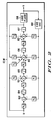
- FIG. 1 illustrates the fourth order 6 bit SDM 17, 18.
- the SDM 17, 18 has a first summing node 100 having a first and second input and an output; a second summing node 101 having a first, second and third input and an output; a third summing node 102 having a first, second, third and fourth input and an output and a fourth summing node 103 having a first, second and third input and an output.
- the SDM 17, 18 additionally has a first, second, third and fourth integrator 104, 105, 106, 107, that act as integrating elements, a 6 bit quantiser 108 and a 6 bit DAC 109.
- An analog signal is input to the first, second and third summing nodes 100, 101, 102 via respective gain coefficient elements b 0 , e 1 and e 2 .
- the output of the first summing node 100 is coupled to the input of the first integrator 104, while the output of the first integrator 104 is coupled to an input of the second summing node 101 via a gain coefficient element b 1 .
- the output of the second summing node 101 is coupled to the input of the second integrator 105, while the output of the second integrator 105 is coupled to an input of the third summing node 102.
- the output of the third summing node 102 is coupled to the input of the third integrator 106, while the output of the third integrator 106 is coupled to the fourth summing node 103.
- the output of the fourth summing node 103 is coupled to the input of the fourth integrator 107, while the output of the fourth integrator 107, a noise shaped analog signal, is coupled to the input of the 6 bit quantiser 108 and is also feedback to an input of the third and fourth summing nodes 102, 103 via respective gain coefficient elements r 2 and r 3 .
- the output of the 6 bit quantiser 108, a digital representation of the noise shaped analog signal is coupled to the input of the decimator filter 19, 20 and to the input of the 6 bit DAC 109.
- the output of the 6 bit DAC 109 is feedback to an input of the first, second, third and fourth summing node 100, 101, 102, 103 via respective gain coefficient elements a 0 , a 1 , a 2 and
- the first, second, third and fourth summing nodes 100, 101, 102, 103 and the first, second third and fourth integrators 104, 105, 106, 107, and the 6 bit DAC 109 and the gain coefficient elements a0, a1, a 2 , a 3 , b 0 , b 1 , b 2 , b 3 , e 1 , e 2 , r 2 and r 3 are arranged, as described above, to provide a fourth order SDM and provide an appropriate noise shaping function, as is well known to a person skilled in the art.
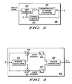
- Figure 3 illustrates the 6 bit flash quantiser 108.
- the 6 bit quantiser 108 includes a 6 bit flash ADC 200, where the flash ADC 200 compares the input analog voltage to 2 6 -1 threshold voltages at periodic intervals to generate a digital representation of the analog signal.
- the periodic intervals are equal to the period of the over sampling frequency, itself determined by the OSR required to achieve the wanted resolution. In the SDM of fig. 2 the over sampling frequency is 80MHz and the sampling intervals equals 12.5ns.
- the 6 bit flash ADC 200 performs the voltage comparison using 2 6 -1 comparators (not shown) (i.e. provides 63 quantization levels) where the dynamic range of the flash ADC 200 is dependent upon the bit size of the quantizer.
- the comparator outputs i.e.
- thermometric to binary converter 201 converts the 2 6 -1 digital input lines into a representative 6 bit digital word that forms the output of the quantiser 108.
- the 6 bit digital output of the thermometric to binary converter 201 is connected to both a control circuit 202, which forms part of the ADC, and the decimation filter 19, 20.
- control circuit 202 includes a window circuit, a first summing node 204 having a first and second input and an output, a second summing node 205 having a first and second input and an output, a first and second latch 206, 207 and a feedback circuit having an enable controller 208.
- the 6 bit digital output of the thermometric to binary converter 201 is connected to the first inputs of the first and second summing nodes 204, 205 and to an input of the window calculator 203. Additionally, outputs from the window calculator 203 are fed to the second inputs of the first and second summing nodes 204, 205. The outputs of the respective first and second summing nodes 204, 205 are coupled to the respective first and second latches 206, 207. The first and second latches 206, 207 are arranged to store a value of a digital sample value output from the respective first and second summing nodes 204, 205.
- the window calculator 203 is arranged to store or calculate the predicted size of the variation window of the signal for the next sample of the analog signal using the value of the current sample and, if necessary, previous samples of the analog signal, in conjunction with predetermined criteria of the analog signal, as described below,.
- Half of the variation window as calculated by the window calculator 203 is decreased by one unit and provided to the second input of the first summing node 204, which adds the value to the current sample value and outputs the upper boundary value, which is stored in the first latch 206.
- Half of the variation window as calculated by the window calculator 203 is decreased by one unit and provided to the second input of the second summing node 205, which subtracts the value from the current sample value outputs the lower boundary value, which is stored in the second latch 207.
- the modified sample values are fed to the enable controller 208 that sends control signals to the flash ADC, for the next sample, to disable comparators that have a voltage threshold range outside the upper and lower boundary values, thereby avoiding unnecessary power consumption by not having comparators enabled that will not be needed.
- the window calculator 203 determines the variation window according to the most suitable algorithm for the receiver that the SDM 17, 18 is embedded within.
- the window calculator stores a pre-determined value that has been calculated according to the properties of the received signal, to the attenuation provided versus frequency by the anti-aliasing filter in front of the SDM, to the OSR and to the SDM Signal Transfer Function.
- the variation window is calculated to be equal to 19 based upon the above criteria. As described above, this value is then stored in the window calculator 203 whatever the current sample value at the thermometric to binary converter output.
- the output of nodes 204 and 205 is used to enable comparators 4 to 20 (i.e. sample value of A minus one plus and minus 8) for the next sample, where a sample value of 7 is actually measured.
- the output of nodes 204 and 205 is used to enable comparators 20 to 31 (i.e. sample value of B minus one plus 3 and minus 8) for the next sample, where a sample value of 29 is actually measured. It may be noticed that 8 comparators instead of 3 should have been enabled above the value of the current sample according to a generic rule of the present invention. However, as there are no comparators beyond the comparator number 31 no more than 3 comparators can be enabled in this particular case. This aspect is taken into account by the enabling controller 208.
- the window calculator 203 which in this embodiment may only need to be a few gates, calculates a predicted variation in sample value based upon well bounded characteristics associated with a SDM processed signal, for example the definition of the SDM input range; by the anti-alias filtering used in front of the SDM; by the OSR; and by the SDM signal transfer function.
- the window calculator 203 could be arranged to use other types of interpolation, for example a predictive algorithm.
- Figure 7 illustrates an alternative embodiment, where the output of the 6 bit flash ADC 200 is provided directly to the control circuit 202.
- the control circuit 202 in this embodiment operates as described above.
- the quantiser 108 could be arranged such that the voltage threshold for the comparators of the flash ADC could be changed based upon the control signal provided by the feedback circuit. Such that a reduced number of comparators could be used that are all enabled such that for a small predicted change in sample value the voltage threshold for the comparators could be lowered, however, for a large predicted change in sample value the voltage threshold for the comparators could be increased.
- the disclosed subject matter may be modified in numerous ways and may assume may embodiments other than the preferred form specifically set out as described above, for example the ADC of the present invention could be used in applications other than a radiotelephone and a WLAN such as video signal processing, medical imaging and radar detection systems, the ADC could be used in a sigma-delta modulator other than fourth order sigma-delta modulator, an ADC according to the present invention does not need to be a 6 bit ADC, the window calculator could be implement in alternative ways, for example a digital signal processor.
Landscapes
- Engineering & Computer Science (AREA)
- Theoretical Computer Science (AREA)
- Analogue/Digital Conversion (AREA)
- Compression, Expansion, Code Conversion, And Decoders (AREA)
Applications Claiming Priority (2)
| Application Number | Priority Date | Filing Date | Title |
|---|---|---|---|
| GB0311992A GB2402006B (en) | 2003-05-23 | 2003-05-23 | Analog to digital converter |
| GB0311992 | 2003-05-23 |
Publications (3)
| Publication Number | Publication Date |
|---|---|
| EP1480342A2 true EP1480342A2 (fr) | 2004-11-24 |
| EP1480342A3 EP1480342A3 (fr) | 2005-01-19 |
| EP1480342B1 EP1480342B1 (fr) | 2009-03-18 |
Family
ID=9958727
Family Applications (1)
| Application Number | Title | Priority Date | Filing Date |
|---|---|---|---|
| EP04011998A Expired - Lifetime EP1480342B1 (fr) | 2003-05-23 | 2004-05-20 | Convertisseur analogique-numérique |
Country Status (5)
| Country | Link |
|---|---|
| US (1) | US7079068B2 (fr) |
| EP (1) | EP1480342B1 (fr) |
| AT (1) | ATE426270T1 (fr) |
| DE (1) | DE602004020015D1 (fr) |
| GB (1) | GB2402006B (fr) |
Cited By (6)
| Publication number | Priority date | Publication date | Assignee | Title |
|---|---|---|---|---|
| WO2009120506A1 (fr) * | 2008-03-28 | 2009-10-01 | Motorola, Inc. | Procédé et système d'exploitation d'un comparateur |
| US7969339B2 (en) | 2006-03-23 | 2011-06-28 | Freescale Semiconductor, Inc. | Electronic device and integrated circuit comprising a delta-sigma converter and method therefor |
| US9100041B1 (en) | 2014-04-30 | 2015-08-04 | Dialog Semiconductor (Uk) Limited | Flash converter capacitance reduction method |
| CN105340182A (zh) * | 2013-06-27 | 2016-02-17 | 赛灵思公司 | 用于高速模数转换的开窗 |
| CN106464263A (zh) * | 2014-04-17 | 2017-02-22 | 塞瑞斯逻辑公司 | 具有动态窗口长度的比较器跟踪控制方案 |
| WO2018195337A1 (fr) * | 2017-04-21 | 2018-10-25 | Abhishek Bandyopadhyay | Quantificateur flash efficace pour convertisseur delta sigma |
Families Citing this family (18)
| Publication number | Priority date | Publication date | Assignee | Title |
|---|---|---|---|---|
| US7262724B2 (en) * | 2005-03-31 | 2007-08-28 | Freescale Semiconductor, Inc. | System and method for adjusting dynamic range of analog-to-digital converter |
| US7973689B2 (en) * | 2008-09-16 | 2011-07-05 | Semtech Corporation | Bandpass multi-bit sigma-delta analog to digital conversion |
| US8212699B1 (en) | 2008-09-16 | 2012-07-03 | Semtech Corporation | System and method for extending the overload range of a sigma delta ADC system by providing over-range quantization levels |
| US9130584B1 (en) * | 2010-01-05 | 2015-09-08 | Syntropy Systems, Llc | Multi-mode sampling/quantization converters |
| US9419637B1 (en) | 2010-01-05 | 2016-08-16 | Syntropy Systems, Llc | Multi-mode sampling/quantization converters |
| US8629899B2 (en) * | 2009-08-06 | 2014-01-14 | Qualcomm Incorporated | Transforming video data in accordance with human visual system feedback metrics |
| US8878912B2 (en) * | 2009-08-06 | 2014-11-04 | Qualcomm Incorporated | Encapsulating three-dimensional video data in accordance with transport protocols |
| US9083958B2 (en) * | 2009-08-06 | 2015-07-14 | Qualcomm Incorporated | Transforming video data in accordance with three dimensional input formats |
| US8009072B2 (en) * | 2009-12-19 | 2011-08-30 | General Electric Company | Predictive analog-to-digital converter and methods thereof |
| US9654128B2 (en) | 2010-01-05 | 2017-05-16 | Syntropy Systems, Llc | Multi-mode sampling/quantization converters |
| JP5905825B2 (ja) * | 2010-09-10 | 2016-04-20 | 日本電気株式会社 | 送信機、制御方法、コンピュータプログラム、およびδς変調器 |
| US8325073B2 (en) | 2010-11-30 | 2012-12-04 | Qualcomm Incorporated | Performing enhanced sigma-delta modulation |
| US8471749B2 (en) | 2011-07-18 | 2013-06-25 | Freescale Semiconductor, Inc. | Comparator |
| US8836566B2 (en) | 2013-02-21 | 2014-09-16 | Freescale Semiconductor, Inc. | Low power quantizer for analog to digital converter |
| US9221679B2 (en) | 2013-03-12 | 2015-12-29 | Freescale Semiconductor, Inc. | Compensation and calibration for MEMS devices |
| US9148169B2 (en) | 2014-02-25 | 2015-09-29 | Freescale Semiconductor, Inc. | Multiple bit sigma-delta modulator with a common mode compensated quantizer |
| US9621175B2 (en) | 2015-02-11 | 2017-04-11 | Syntropy Systems, Llc | Sampling/quantization converters |
| US11722146B1 (en) * | 2022-01-21 | 2023-08-08 | Nxp B.V. | Correction of sigma-delta analog-to-digital converters (ADCs) using neural networks |
Family Cites Families (12)
| Publication number | Priority date | Publication date | Assignee | Title |
|---|---|---|---|---|
| US5327131A (en) * | 1991-11-07 | 1994-07-05 | Kawasaki Steel Corporation | Parallel A/D converter having comparator threshold voltages defined by MOS transistor geometries |
| US5727023A (en) * | 1992-10-27 | 1998-03-10 | Ericsson Inc. | Apparatus for and method of speech digitizing |
| US5648779A (en) * | 1994-12-09 | 1997-07-15 | Advanced Micro Devices, Inc. | Sigma-delta modulator having reduced delay from input to output |
| US5790061A (en) * | 1995-02-24 | 1998-08-04 | Nec Corporation | Adaptive A/D converting device for adaptively converting and input analog signal into an output digital signal having a constant quantizing error |
| US5751615A (en) * | 1995-11-14 | 1998-05-12 | Advanced Micro Devices, Inc. | Implementation of a digital decimation filter and method |
| US6546044B1 (en) * | 1996-10-11 | 2003-04-08 | Ericsson Inc. | Dual-mode radiotelephone apparatus for digital or analog modulation |
| US6097251A (en) * | 1998-05-29 | 2000-08-01 | Telefonaktiebolaget Lm Ericsson | Pre-recorded sigma delta values for power amplifier control |
| EP0940922B1 (fr) * | 1998-03-03 | 2002-12-04 | Motorola Semiconducteurs S.A. | Synthétiseur de fréquence |
| US6081219A (en) * | 1998-05-05 | 2000-06-27 | Lucent Technology, Inc. | Power saving arrangement for a flash A/D converter |
| US6101224A (en) * | 1998-10-07 | 2000-08-08 | Telefonaktiebolaget Lm Ericsson | Method and apparatus for generating a linearly modulated signal using polar modulation |
| US6188347B1 (en) * | 1999-07-12 | 2001-02-13 | National Instruments Corporation | Analog-to-digital conversion system and method with reduced sparkle codes |
| US6373423B1 (en) * | 1999-12-14 | 2002-04-16 | National Instruments Corporation | Flash analog-to-digital conversion system and method with reduced comparators |
-
2003
- 2003-05-23 GB GB0311992A patent/GB2402006B/en not_active Expired - Fee Related
-
2004
- 2004-05-20 AT AT04011998T patent/ATE426270T1/de not_active IP Right Cessation
- 2004-05-20 EP EP04011998A patent/EP1480342B1/fr not_active Expired - Lifetime
- 2004-05-20 DE DE602004020015T patent/DE602004020015D1/de not_active Expired - Lifetime
- 2004-05-21 US US10/851,608 patent/US7079068B2/en not_active Expired - Lifetime
Cited By (12)
| Publication number | Priority date | Publication date | Assignee | Title |
|---|---|---|---|---|
| US7969339B2 (en) | 2006-03-23 | 2011-06-28 | Freescale Semiconductor, Inc. | Electronic device and integrated circuit comprising a delta-sigma converter and method therefor |
| WO2009120506A1 (fr) * | 2008-03-28 | 2009-10-01 | Motorola, Inc. | Procédé et système d'exploitation d'un comparateur |
| CN105340182A (zh) * | 2013-06-27 | 2016-02-17 | 赛灵思公司 | 用于高速模数转换的开窗 |
| EP3014773A1 (fr) * | 2013-06-27 | 2016-05-04 | Xilinx, Inc. | Fenêtrage pour conversion analogique à numérique à haute vitesse |
| CN105340182B (zh) * | 2013-06-27 | 2019-01-01 | 赛灵思公司 | 用于高速模数转换的开窗 |
| CN106464263A (zh) * | 2014-04-17 | 2017-02-22 | 塞瑞斯逻辑公司 | 具有动态窗口长度的比较器跟踪控制方案 |
| EP3132542A4 (fr) * | 2014-04-17 | 2017-12-27 | Cirrus Logic, Inc. | Schéma de commande de suivi de comparateur ayant une longueur de fenêtre dynamique |
| CN106464263B (zh) * | 2014-04-17 | 2020-06-12 | 塞瑞斯逻辑公司 | 具有动态窗口长度的比较器跟踪控制方案 |
| US9100041B1 (en) | 2014-04-30 | 2015-08-04 | Dialog Semiconductor (Uk) Limited | Flash converter capacitance reduction method |
| EP2940874A1 (fr) * | 2014-04-30 | 2015-11-04 | Dialog Semiconductor GmbH | Procédé de réduction de capacité de convertisseur parallèle |
| WO2018195337A1 (fr) * | 2017-04-21 | 2018-10-25 | Abhishek Bandyopadhyay | Quantificateur flash efficace pour convertisseur delta sigma |
| US10284221B2 (en) | 2017-04-21 | 2019-05-07 | Analog Devices, Inc. | Power-efficient flash quantizer for delta sigma converter |
Also Published As
| Publication number | Publication date |
|---|---|
| GB2402006B (en) | 2005-08-10 |
| ATE426270T1 (de) | 2009-04-15 |
| US7079068B2 (en) | 2006-07-18 |
| GB2402006A (en) | 2004-11-24 |
| DE602004020015D1 (de) | 2009-04-30 |
| GB0311992D0 (en) | 2003-07-02 |
| US20040233091A1 (en) | 2004-11-25 |
| EP1480342A3 (fr) | 2005-01-19 |
| EP1480342B1 (fr) | 2009-03-18 |
Similar Documents
| Publication | Publication Date | Title |
|---|---|---|
| US7079068B2 (en) | Analog to digital converter | |
| KR100923481B1 (ko) | 전류 모드 동적 요소 정합 및 동적 요소 정합 결정 로직을 포함하는 멀티비트 양자화 시그마 델타 변조기 | |
| US6727833B2 (en) | Adaptive ΣΔ modulation with one-bit quantization | |
| EP0887939B1 (fr) | Procédé d'échantillonnage, de conversion à la bas, et de numérisation d'un signal à bande passante à l'aide d'un codeur numérique à prédiction | |
| US7576671B2 (en) | Mismatch-shaping dynamic element matching systems and methods for multi-bit sigma-delta data converters | |
| CN101427471B (zh) | 使用模拟-数字δ-∑调制器的信号处理系统及方法 | |
| US7339510B2 (en) | Accumulator for adaptive sigma-delta modulation | |
| JP6375119B2 (ja) | アナログ−デジタル変換器のための低電力量子化器 | |
| US9240801B2 (en) | Analog-to-digital converter | |
| US20040036636A1 (en) | Tone-free dithering methods for sigma-delta DAC | |
| US7969339B2 (en) | Electronic device and integrated circuit comprising a delta-sigma converter and method therefor | |
| EP3245740B1 (fr) | Technique de tramage efficace pour convertisseurs analogique-numérique sigma-delta | |
| Ledzius et al. | The basis and architecture for the reduction of tones in a sigma-delta DAC | |
| KR101593729B1 (ko) | 입력 신호로부터 rf 신호를 합성하기 위한 방법, 델타-시그마 변조기 및 집적 회로 | |
| JP2006254261A (ja) | Σδ型a/d変換回路を内蔵した通信用半導体集積回路 | |
| Torreño et al. | A noise coupled ΣΔ architecture using a non uniform quantizer | |
| EP1665544B1 (fr) | Accumulateur de modulation sigma-delta adaptative | |
| Vera et al. | DAC mismatch shaping in Discrete Time Sigma Delta ADCs with non uniform quantizer | |
| US8102290B2 (en) | Sigma-delta modulator | |
| JP4549264B2 (ja) | デルタシグマ変調回路及びそれを備えたスイッチングアンプ |
Legal Events
| Date | Code | Title | Description |
|---|---|---|---|
| PUAI | Public reference made under article 153(3) epc to a published international application that has entered the european phase |
Free format text: ORIGINAL CODE: 0009012 |
|
| 17P | Request for examination filed |
Effective date: 20040520 |
|
| AK | Designated contracting states |
Kind code of ref document: A2 Designated state(s): AT BE BG CH CY CZ DE DK EE ES FI FR GB GR HU IE IT LI LU MC NL PL PT RO SE SI SK TR |
|
| AX | Request for extension of the european patent |
Extension state: AL HR LT LV MK |
|
| PUAL | Search report despatched |
Free format text: ORIGINAL CODE: 0009013 |
|
| AK | Designated contracting states |
Kind code of ref document: A3 Designated state(s): AT BE BG CH CY CZ DE DK EE ES FI FR GB GR HU IE IT LI LU MC NL PL PT RO SE SI SK TR |
|
| AX | Request for extension of the european patent |
Extension state: AL HR LT LV MK |
|
| AKX | Designation fees paid |
Designated state(s): AT BE BG CH CY CZ DE DK EE ES FI FR GB GR HU IE IT LI LU MC NL PL PT RO SE SI SK TR |
|
| 17Q | First examination report despatched |
Effective date: 20060421 |
|
| GRAJ | Information related to disapproval of communication of intention to grant by the applicant or resumption of examination proceedings by the epo deleted |
Free format text: ORIGINAL CODE: EPIDOSDIGR1 |
|
| GRAP | Despatch of communication of intention to grant a patent |
Free format text: ORIGINAL CODE: EPIDOSNIGR1 |
|
| GRAP | Despatch of communication of intention to grant a patent |
Free format text: ORIGINAL CODE: EPIDOSNIGR1 |
|
| GRAS | Grant fee paid |
Free format text: ORIGINAL CODE: EPIDOSNIGR3 |
|
| GRAA | (expected) grant |
Free format text: ORIGINAL CODE: 0009210 |
|
| AK | Designated contracting states |
Kind code of ref document: B1 Designated state(s): AT BE BG CH CY CZ DE DK EE ES FI FR GB GR HU IE IT LI LU MC NL PL PT RO SE SI SK TR |
|
| REG | Reference to a national code |
Ref country code: GB Ref legal event code: FG4D |
|
| REG | Reference to a national code |
Ref country code: CH Ref legal event code: EP |
|
| REG | Reference to a national code |
Ref country code: IE Ref legal event code: FG4D |
|
| REF | Corresponds to: |
Ref document number: 602004020015 Country of ref document: DE Date of ref document: 20090430 Kind code of ref document: P |
|
| PG25 | Lapsed in a contracting state [announced via postgrant information from national office to epo] |
Ref country code: SI Free format text: LAPSE BECAUSE OF FAILURE TO SUBMIT A TRANSLATION OF THE DESCRIPTION OR TO PAY THE FEE WITHIN THE PRESCRIBED TIME-LIMIT Effective date: 20090318 Ref country code: FI Free format text: LAPSE BECAUSE OF FAILURE TO SUBMIT A TRANSLATION OF THE DESCRIPTION OR TO PAY THE FEE WITHIN THE PRESCRIBED TIME-LIMIT Effective date: 20090318 Ref country code: NL Free format text: LAPSE BECAUSE OF FAILURE TO SUBMIT A TRANSLATION OF THE DESCRIPTION OR TO PAY THE FEE WITHIN THE PRESCRIBED TIME-LIMIT Effective date: 20090318 |
|
| PG25 | Lapsed in a contracting state [announced via postgrant information from national office to epo] |
Ref country code: SE Free format text: LAPSE BECAUSE OF FAILURE TO SUBMIT A TRANSLATION OF THE DESCRIPTION OR TO PAY THE FEE WITHIN THE PRESCRIBED TIME-LIMIT Effective date: 20090618 Ref country code: PL Free format text: LAPSE BECAUSE OF FAILURE TO SUBMIT A TRANSLATION OF THE DESCRIPTION OR TO PAY THE FEE WITHIN THE PRESCRIBED TIME-LIMIT Effective date: 20090318 Ref country code: AT Free format text: LAPSE BECAUSE OF FAILURE TO SUBMIT A TRANSLATION OF THE DESCRIPTION OR TO PAY THE FEE WITHIN THE PRESCRIBED TIME-LIMIT Effective date: 20090318 |
|
| NLV1 | Nl: lapsed or annulled due to failure to fulfill the requirements of art. 29p and 29m of the patents act | ||
| PG25 | Lapsed in a contracting state [announced via postgrant information from national office to epo] |
Ref country code: BE Free format text: LAPSE BECAUSE OF FAILURE TO SUBMIT A TRANSLATION OF THE DESCRIPTION OR TO PAY THE FEE WITHIN THE PRESCRIBED TIME-LIMIT Effective date: 20090318 |
|
| PG25 | Lapsed in a contracting state [announced via postgrant information from national office to epo] |
Ref country code: ES Free format text: LAPSE BECAUSE OF FAILURE TO SUBMIT A TRANSLATION OF THE DESCRIPTION OR TO PAY THE FEE WITHIN THE PRESCRIBED TIME-LIMIT Effective date: 20090629 Ref country code: CZ Free format text: LAPSE BECAUSE OF FAILURE TO SUBMIT A TRANSLATION OF THE DESCRIPTION OR TO PAY THE FEE WITHIN THE PRESCRIBED TIME-LIMIT Effective date: 20090318 Ref country code: EE Free format text: LAPSE BECAUSE OF FAILURE TO SUBMIT A TRANSLATION OF THE DESCRIPTION OR TO PAY THE FEE WITHIN THE PRESCRIBED TIME-LIMIT Effective date: 20090318 Ref country code: PT Free format text: LAPSE BECAUSE OF FAILURE TO SUBMIT A TRANSLATION OF THE DESCRIPTION OR TO PAY THE FEE WITHIN THE PRESCRIBED TIME-LIMIT Effective date: 20090826 |
|
| PG25 | Lapsed in a contracting state [announced via postgrant information from national office to epo] |
Ref country code: SK Free format text: LAPSE BECAUSE OF FAILURE TO SUBMIT A TRANSLATION OF THE DESCRIPTION OR TO PAY THE FEE WITHIN THE PRESCRIBED TIME-LIMIT Effective date: 20090318 Ref country code: RO Free format text: LAPSE BECAUSE OF FAILURE TO SUBMIT A TRANSLATION OF THE DESCRIPTION OR TO PAY THE FEE WITHIN THE PRESCRIBED TIME-LIMIT Effective date: 20090318 |
|
| PG25 | Lapsed in a contracting state [announced via postgrant information from national office to epo] |
Ref country code: MC Free format text: LAPSE BECAUSE OF NON-PAYMENT OF DUE FEES Effective date: 20090531 |
|
| REG | Reference to a national code |
Ref country code: CH Ref legal event code: PL |
|
| PLBE | No opposition filed within time limit |
Free format text: ORIGINAL CODE: 0009261 |
|
| STAA | Information on the status of an ep patent application or granted ep patent |
Free format text: STATUS: NO OPPOSITION FILED WITHIN TIME LIMIT |
|
| PG25 | Lapsed in a contracting state [announced via postgrant information from national office to epo] |
Ref country code: CH Free format text: LAPSE BECAUSE OF NON-PAYMENT OF DUE FEES Effective date: 20090531 Ref country code: BG Free format text: LAPSE BECAUSE OF FAILURE TO SUBMIT A TRANSLATION OF THE DESCRIPTION OR TO PAY THE FEE WITHIN THE PRESCRIBED TIME-LIMIT Effective date: 20090618 Ref country code: LI Free format text: LAPSE BECAUSE OF NON-PAYMENT OF DUE FEES Effective date: 20090531 Ref country code: DK Free format text: LAPSE BECAUSE OF FAILURE TO SUBMIT A TRANSLATION OF THE DESCRIPTION OR TO PAY THE FEE WITHIN THE PRESCRIBED TIME-LIMIT Effective date: 20090318 |
|
| 26N | No opposition filed |
Effective date: 20091221 |
|
| REG | Reference to a national code |
Ref country code: IE Ref legal event code: MM4A |
|
| PG25 | Lapsed in a contracting state [announced via postgrant information from national office to epo] |
Ref country code: IE Free format text: LAPSE BECAUSE OF NON-PAYMENT OF DUE FEES Effective date: 20090520 |
|
| PG25 | Lapsed in a contracting state [announced via postgrant information from national office to epo] |
Ref country code: GR Free format text: LAPSE BECAUSE OF FAILURE TO SUBMIT A TRANSLATION OF THE DESCRIPTION OR TO PAY THE FEE WITHIN THE PRESCRIBED TIME-LIMIT Effective date: 20090619 |
|
| PG25 | Lapsed in a contracting state [announced via postgrant information from national office to epo] |
Ref country code: IT Free format text: LAPSE BECAUSE OF FAILURE TO SUBMIT A TRANSLATION OF THE DESCRIPTION OR TO PAY THE FEE WITHIN THE PRESCRIBED TIME-LIMIT Effective date: 20090318 |
|
| PG25 | Lapsed in a contracting state [announced via postgrant information from national office to epo] |
Ref country code: LU Free format text: LAPSE BECAUSE OF NON-PAYMENT OF DUE FEES Effective date: 20090520 |
|
| PG25 | Lapsed in a contracting state [announced via postgrant information from national office to epo] |
Ref country code: HU Free format text: LAPSE BECAUSE OF FAILURE TO SUBMIT A TRANSLATION OF THE DESCRIPTION OR TO PAY THE FEE WITHIN THE PRESCRIBED TIME-LIMIT Effective date: 20090919 |
|
| PG25 | Lapsed in a contracting state [announced via postgrant information from national office to epo] |
Ref country code: TR Free format text: LAPSE BECAUSE OF FAILURE TO SUBMIT A TRANSLATION OF THE DESCRIPTION OR TO PAY THE FEE WITHIN THE PRESCRIBED TIME-LIMIT Effective date: 20090318 |
|
| PG25 | Lapsed in a contracting state [announced via postgrant information from national office to epo] |
Ref country code: CY Free format text: LAPSE BECAUSE OF FAILURE TO SUBMIT A TRANSLATION OF THE DESCRIPTION OR TO PAY THE FEE WITHIN THE PRESCRIBED TIME-LIMIT Effective date: 20090318 |
|
| PGFP | Annual fee paid to national office [announced via postgrant information from national office to epo] |
Ref country code: GB Payment date: 20140527 Year of fee payment: 11 |
|
| PGFP | Annual fee paid to national office [announced via postgrant information from national office to epo] |
Ref country code: FR Payment date: 20140519 Year of fee payment: 11 |
|
| GBPC | Gb: european patent ceased through non-payment of renewal fee |
Effective date: 20150520 |
|
| REG | Reference to a national code |
Ref country code: FR Ref legal event code: ST Effective date: 20160129 |
|
| REG | Reference to a national code |
Ref country code: DE Ref legal event code: R081 Ref document number: 602004020015 Country of ref document: DE Owner name: NORTH STAR INNOVATIONS INC., COSTA MESA, US Free format text: FORMER OWNER: FREESCALE SEMICONDUCTOR INC. (N.D.GES.D. STAATES DELAWARE), AUSTIN, TEX., US |
|
| PG25 | Lapsed in a contracting state [announced via postgrant information from national office to epo] |
Ref country code: GB Free format text: LAPSE BECAUSE OF NON-PAYMENT OF DUE FEES Effective date: 20150520 |
|
| PG25 | Lapsed in a contracting state [announced via postgrant information from national office to epo] |
Ref country code: FR Free format text: LAPSE BECAUSE OF NON-PAYMENT OF DUE FEES Effective date: 20150601 |
|
| PGFP | Annual fee paid to national office [announced via postgrant information from national office to epo] |
Ref country code: DE Payment date: 20160527 Year of fee payment: 13 |
|
| REG | Reference to a national code |
Ref country code: DE Ref legal event code: R119 Ref document number: 602004020015 Country of ref document: DE |
|
| PG25 | Lapsed in a contracting state [announced via postgrant information from national office to epo] |
Ref country code: DE Free format text: LAPSE BECAUSE OF NON-PAYMENT OF DUE FEES Effective date: 20171201 |