EP1481806B1 - Tête d'impression à jet d'encre et sa méthode de fabrication - Google Patents
Tête d'impression à jet d'encre et sa méthode de fabrication Download PDFInfo
- Publication number
- EP1481806B1 EP1481806B1 EP04253091A EP04253091A EP1481806B1 EP 1481806 B1 EP1481806 B1 EP 1481806B1 EP 04253091 A EP04253091 A EP 04253091A EP 04253091 A EP04253091 A EP 04253091A EP 1481806 B1 EP1481806 B1 EP 1481806B1
- Authority
- EP
- European Patent Office
- Prior art keywords
- ink
- layer
- forming
- nozzle
- substrate
- Prior art date
- Legal status (The legal status is an assumption and is not a legal conclusion. Google has not performed a legal analysis and makes no representation as to the accuracy of the status listed.)
- Expired - Lifetime
Links
Images







Classifications
-
- B—PERFORMING OPERATIONS; TRANSPORTING
- B41—PRINTING; LINING MACHINES; TYPEWRITERS; STAMPS
- B41J—TYPEWRITERS; SELECTIVE PRINTING MECHANISMS, i.e. MECHANISMS PRINTING OTHERWISE THAN FROM A FORME; CORRECTION OF TYPOGRAPHICAL ERRORS
- B41J2/00—Typewriters or selective printing mechanisms characterised by the printing or marking process for which they are designed
- B41J2/005—Typewriters or selective printing mechanisms characterised by the printing or marking process for which they are designed characterised by bringing liquid or particles selectively into contact with a printing material
- B41J2/01—Ink jet
- B41J2/135—Nozzles
- B41J2/16—Production of nozzles
- B41J2/1621—Manufacturing processes
- B41J2/164—Manufacturing processes thin film formation
- B41J2/1646—Manufacturing processes thin film formation thin film formation by sputtering
-
- B—PERFORMING OPERATIONS; TRANSPORTING
- B41—PRINTING; LINING MACHINES; TYPEWRITERS; STAMPS
- B41J—TYPEWRITERS; SELECTIVE PRINTING MECHANISMS, i.e. MECHANISMS PRINTING OTHERWISE THAN FROM A FORME; CORRECTION OF TYPOGRAPHICAL ERRORS
- B41J2/00—Typewriters or selective printing mechanisms characterised by the printing or marking process for which they are designed
- B41J2/315—Typewriters or selective printing mechanisms characterised by the printing or marking process for which they are designed characterised by selective application of heat to a heat sensitive printing or impression-transfer material
- B41J2/32—Typewriters or selective printing mechanisms characterised by the printing or marking process for which they are designed characterised by selective application of heat to a heat sensitive printing or impression-transfer material using thermal heads
- B41J2/335—Structure of thermal heads
-
- B—PERFORMING OPERATIONS; TRANSPORTING
- B41—PRINTING; LINING MACHINES; TYPEWRITERS; STAMPS
- B41J—TYPEWRITERS; SELECTIVE PRINTING MECHANISMS, i.e. MECHANISMS PRINTING OTHERWISE THAN FROM A FORME; CORRECTION OF TYPOGRAPHICAL ERRORS
- B41J2/00—Typewriters or selective printing mechanisms characterised by the printing or marking process for which they are designed
- B41J2/005—Typewriters or selective printing mechanisms characterised by the printing or marking process for which they are designed characterised by bringing liquid or particles selectively into contact with a printing material
- B41J2/01—Ink jet
- B41J2/135—Nozzles
- B41J2/16—Production of nozzles
- B41J2/1601—Production of bubble jet print heads
-
- B—PERFORMING OPERATIONS; TRANSPORTING
- B41—PRINTING; LINING MACHINES; TYPEWRITERS; STAMPS
- B41J—TYPEWRITERS; SELECTIVE PRINTING MECHANISMS, i.e. MECHANISMS PRINTING OTHERWISE THAN FROM A FORME; CORRECTION OF TYPOGRAPHICAL ERRORS
- B41J2/00—Typewriters or selective printing mechanisms characterised by the printing or marking process for which they are designed
- B41J2/005—Typewriters or selective printing mechanisms characterised by the printing or marking process for which they are designed characterised by bringing liquid or particles selectively into contact with a printing material
- B41J2/01—Ink jet
- B41J2/135—Nozzles
- B41J2/16—Production of nozzles
- B41J2/1621—Manufacturing processes
- B41J2/1626—Manufacturing processes etching
- B41J2/1628—Manufacturing processes etching dry etching
-
- B—PERFORMING OPERATIONS; TRANSPORTING
- B41—PRINTING; LINING MACHINES; TYPEWRITERS; STAMPS
- B41J—TYPEWRITERS; SELECTIVE PRINTING MECHANISMS, i.e. MECHANISMS PRINTING OTHERWISE THAN FROM A FORME; CORRECTION OF TYPOGRAPHICAL ERRORS
- B41J2/00—Typewriters or selective printing mechanisms characterised by the printing or marking process for which they are designed
- B41J2/005—Typewriters or selective printing mechanisms characterised by the printing or marking process for which they are designed characterised by bringing liquid or particles selectively into contact with a printing material
- B41J2/01—Ink jet
- B41J2/135—Nozzles
- B41J2/16—Production of nozzles
- B41J2/1621—Manufacturing processes
- B41J2/1626—Manufacturing processes etching
- B41J2/1629—Manufacturing processes etching wet etching
-
- B—PERFORMING OPERATIONS; TRANSPORTING
- B41—PRINTING; LINING MACHINES; TYPEWRITERS; STAMPS
- B41J—TYPEWRITERS; SELECTIVE PRINTING MECHANISMS, i.e. MECHANISMS PRINTING OTHERWISE THAN FROM A FORME; CORRECTION OF TYPOGRAPHICAL ERRORS
- B41J2/00—Typewriters or selective printing mechanisms characterised by the printing or marking process for which they are designed
- B41J2/005—Typewriters or selective printing mechanisms characterised by the printing or marking process for which they are designed characterised by bringing liquid or particles selectively into contact with a printing material
- B41J2/01—Ink jet
- B41J2/135—Nozzles
- B41J2/16—Production of nozzles
- B41J2/1621—Manufacturing processes
- B41J2/1631—Manufacturing processes photolithography
-
- B—PERFORMING OPERATIONS; TRANSPORTING
- B41—PRINTING; LINING MACHINES; TYPEWRITERS; STAMPS
- B41J—TYPEWRITERS; SELECTIVE PRINTING MECHANISMS, i.e. MECHANISMS PRINTING OTHERWISE THAN FROM A FORME; CORRECTION OF TYPOGRAPHICAL ERRORS
- B41J2/00—Typewriters or selective printing mechanisms characterised by the printing or marking process for which they are designed
- B41J2/005—Typewriters or selective printing mechanisms characterised by the printing or marking process for which they are designed characterised by bringing liquid or particles selectively into contact with a printing material
- B41J2/01—Ink jet
- B41J2/135—Nozzles
- B41J2/16—Production of nozzles
- B41J2/1621—Manufacturing processes
- B41J2/1632—Manufacturing processes machining
-
- B—PERFORMING OPERATIONS; TRANSPORTING
- B41—PRINTING; LINING MACHINES; TYPEWRITERS; STAMPS
- B41J—TYPEWRITERS; SELECTIVE PRINTING MECHANISMS, i.e. MECHANISMS PRINTING OTHERWISE THAN FROM A FORME; CORRECTION OF TYPOGRAPHICAL ERRORS
- B41J2/00—Typewriters or selective printing mechanisms characterised by the printing or marking process for which they are designed
- B41J2/005—Typewriters or selective printing mechanisms characterised by the printing or marking process for which they are designed characterised by bringing liquid or particles selectively into contact with a printing material
- B41J2/01—Ink jet
- B41J2/135—Nozzles
- B41J2/16—Production of nozzles
- B41J2/1621—Manufacturing processes
- B41J2/1637—Manufacturing processes molding
- B41J2/1639—Manufacturing processes molding sacrificial molding
-
- B—PERFORMING OPERATIONS; TRANSPORTING
- B41—PRINTING; LINING MACHINES; TYPEWRITERS; STAMPS
- B41J—TYPEWRITERS; SELECTIVE PRINTING MECHANISMS, i.e. MECHANISMS PRINTING OTHERWISE THAN FROM A FORME; CORRECTION OF TYPOGRAPHICAL ERRORS
- B41J2/00—Typewriters or selective printing mechanisms characterised by the printing or marking process for which they are designed
- B41J2/005—Typewriters or selective printing mechanisms characterised by the printing or marking process for which they are designed characterised by bringing liquid or particles selectively into contact with a printing material
- B41J2/01—Ink jet
- B41J2/135—Nozzles
- B41J2/16—Production of nozzles
- B41J2/1621—Manufacturing processes
- B41J2/164—Manufacturing processes thin film formation
- B41J2/1642—Manufacturing processes thin film formation thin film formation by CVD [chemical vapor deposition]
-
- B—PERFORMING OPERATIONS; TRANSPORTING
- B41—PRINTING; LINING MACHINES; TYPEWRITERS; STAMPS
- B41J—TYPEWRITERS; SELECTIVE PRINTING MECHANISMS, i.e. MECHANISMS PRINTING OTHERWISE THAN FROM A FORME; CORRECTION OF TYPOGRAPHICAL ERRORS
- B41J2/00—Typewriters or selective printing mechanisms characterised by the printing or marking process for which they are designed
- B41J2/005—Typewriters or selective printing mechanisms characterised by the printing or marking process for which they are designed characterised by bringing liquid or particles selectively into contact with a printing material
- B41J2/01—Ink jet
- B41J2/135—Nozzles
- B41J2/16—Production of nozzles
- B41J2/1621—Manufacturing processes
- B41J2/164—Manufacturing processes thin film formation
- B41J2/1643—Manufacturing processes thin film formation thin film formation by plating
-
- B—PERFORMING OPERATIONS; TRANSPORTING
- B41—PRINTING; LINING MACHINES; TYPEWRITERS; STAMPS
- B41J—TYPEWRITERS; SELECTIVE PRINTING MECHANISMS, i.e. MECHANISMS PRINTING OTHERWISE THAN FROM A FORME; CORRECTION OF TYPOGRAPHICAL ERRORS
- B41J2/00—Typewriters or selective printing mechanisms characterised by the printing or marking process for which they are designed
- B41J2/005—Typewriters or selective printing mechanisms characterised by the printing or marking process for which they are designed characterised by bringing liquid or particles selectively into contact with a printing material
- B41J2/01—Ink jet
- B41J2/135—Nozzles
- B41J2/14—Structure thereof only for on-demand ink jet heads
- B41J2002/1437—Back shooter
-
- B—PERFORMING OPERATIONS; TRANSPORTING
- B41—PRINTING; LINING MACHINES; TYPEWRITERS; STAMPS
- B41J—TYPEWRITERS; SELECTIVE PRINTING MECHANISMS, i.e. MECHANISMS PRINTING OTHERWISE THAN FROM A FORME; CORRECTION OF TYPOGRAPHICAL ERRORS
- B41J2/00—Typewriters or selective printing mechanisms characterised by the printing or marking process for which they are designed
- B41J2/005—Typewriters or selective printing mechanisms characterised by the printing or marking process for which they are designed characterised by bringing liquid or particles selectively into contact with a printing material
- B41J2/01—Ink jet
- B41J2/135—Nozzles
- B41J2/14—Structure thereof only for on-demand ink jet heads
- B41J2002/14387—Front shooter
Definitions
- the present invention relates to an ink-jet printhead and a method for manufacturing the same, and more particularly, to an ink-jet printhead in which an ink passage is formed in the same plane as an ink chamber to improve ejection performance, a metallic nozzle plate is disposed on a substrate to improve linearity of ink droplets ejected through a nozzle, and heat generated by a heater is effectively dissipated to increase a driving frequency of the printhead, and a method for manufacturing the same.
- inkjet printheads are devices for printing a predetermined color image by ejecting droplets of ink at desired positions on a recording sheet.
- Inkjet printheads are generally categorized into two types according to an ink ejection mechanism.
- One is a thermal inkjet printhead in which a source of heat is employed to form bubbles in ink to eject the ink due to the expansive force of the bubbles.
- the other is a piezoelectric inkjet printhead in which ink is ejected by a pressure applied to the ink due to deformation of a piezoelectric element.
- the ink droplet ejection mechanism of the thermal inkjet printhead will be explained in further detail.
- a current pulse is supplied to a heater which comprises a heating resistor, the heater generates heat such that ink near to the heater is instantaneously heated to approximately 300°C.
- the ink boils to generate bubbles the generated bubbles expand to exert a pressure on the ink filled in an ink chamber. Therefore, the ink around a nozzle is ejected in the form of droplets to the outside of the ink chamber.
- the thermal inkjet printhead is classified into a top-shooting type, a side-shooting type, and a back-shooting type, according to a bubble growing direction and a droplet ejection direction.
- a top-shooting type printhead bubbles grow in the same direction in which ink droplets are ejected.
- a side-shooting type of printhead bubbles grow in a direction perpendicular to a direction in which ink droplets are ejected.
- bubbles grow in a direction opposite to a direction in which ink droplets are ejected.
- the thermal inkjet printhead generally needs to meet the following conditions.
- Third, a refill cycle after ink ejection must be as short as possible to permit high-speed printing. That is, an operating frequency must be high by fast-cooling the heated ink and the heater.
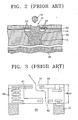
- FIGS. 1 through 3 illustrate the structure of a conventional back-shooting thermal ink-jet printhead.
- FIG. 1 is a perspective view illustrating the structure of an ink-jet printhead disclosed in U.S. Patent No. 5,502,471 .
- an ink-jet printhead 24 has a structure in which a substrate 11 having a nozzle 10 through which ink droplets are ejected and an ink chamber 16 filled with ink to be ejected, a cover plate 3 having a through hole 2 connecting the ink chamber 16 and an ink reservoir 12, and the ink reservoir 12 which supplies ink to the ink chamber 16, are sequentially stacked.
- a heater 42 has a ring shape and is disposed around the nozzle 10 of the substrate 11.
- ink in the ink chamber 16 boils and bubbles are generated.
- the bubbles expand continuously and apply pressure to ink in the ink chamber 16.
- ink is ejected in droplets through the nozzle 10.
- ink is drawn into the ink chamber 16 from the ink reservoir 12 through the through hole 2 formed in the cover plate 3, and the ink chamber 16 is refilled with ink.
- the height of the ink chamber 16 is almost the same as the thickness of the substrate 11, unless a very thin substrate is used, the size of the ink chamber 16 increases. Thus, pressure generated by bubbles for ejecting ink is dispersed by the ink, resulting in degradation of an ejection property. Meanwhile, if a thin substrate is used to reduce the size of the ink chamber 16, it is difficult to process the substrate 11. In other words, the height of the ink chamber 16 in a typical conventional ink-jet printhead is about 10-30 ⁇ m. In order to form an ink chamber having this height, a silicon substrate having a thickness of 10-30 ⁇ m should be used. However, it is impossible to process a silicon substrate having such a thickness using semiconductor processes.
- the substrate 11, the cover plate 3, and the ink reservoir 12 should be bonded to one another.
- a process of manufacturing the ink-jet printhead becomes complicated, and an ink passage, which has a large effect on the ejection property, cannot be made very elaborate.
- FIG. 2 is a cross-sectional view illustrating the structure of an ink-jet printhead disclosed in U.S. Patent No. 5,841,452 .
- a hemispherical ink chamber 15 is formed on a substrate 30 formed of silicon, a manifold 26 which supplies ink to the ink chamber 15 is formed under the substrate 30, and an ink channel 13 which connects the ink chamber 15 and the manifold 26 has a cylindrical shape and is formed between the ink chamber 15 and the manifold 26, perpendicular to the surface of the substrate 30.
- a nozzle plate 20 having a nozzle 21 through which ink droplets 18 are ejected is positioned on the surface of the substrate 30 and forms an upper wall of the ink chamber 15.
- a ring-shaped heater 22 which is adjacent to and surrounds the nozzle 21 is formed in the nozzle plate 20, and an electric wire (not shown) for applying an electric current is connected to the heater 22.
- the size of the ink chamber 15 can be reduced.
- the printhead is manufactured by a batch process without a bonding process, a process of manufacturing the ink-jet printhead is simple.
- the ink channel 13 is positioned in the same line as the nozzle 21, ink flows back toward the ink channel 13 when bubbles are generated, thereby lowering the ejection property.
- the substrate 30 exposed by the nozzle 21 is etched to form the ink chamber 15, the size of the ink chamber can be reduced, but the ink chamber 15 cannot be formed with various different shapes. Thus, it is difficult to form the ink chamber to have an optimum shape.
- FIG. 3 is a cross-sectional view illustrating the structure of an ink-jet printhead disclosed in U.S. Patent No. 6,382,782 .
- the ink-jet printhead has a structure in which a nozzle plate 50 having a nozzle 51, an insulating layer 60 having an ink chamber 61 and an ink channel 62, and a silicon substrate 70 having a manifold 55 for supplying ink to the ink chamber 61, are sequentially stacked.
- the ink chamber 61 since the ink chamber 61 is formed using the insulating layer 60 stacked on the substrate 70, the ink chamber 61 may have a variety of shapes, and backflow of ink can be reduced.
- US 2003/0085957 A1 discloses an ink-jet printhead comprising a field oxide layer and nozzle layers formed over a silicon substrate.
- the field oxide layer is etched to form an elongate ink chamber and the silicon substrate is etched to form an ink manifold.
- the nozzle layers comprise a oxide layers, a heater and a conductor. This document disclosed an ink-jet head according to the preamble of claim 1.
- US 6019457 discloses several nozzle arrangements for ink-jet printheads. Some of these structures include a thermal diffuser, or thermal shunt, formed as part of a layer of metal contacts.
- an ink-jet printhead comprising: a substrate, an ink chamber to be filled with ink to be ejected being formed on a surface of the substrate, a manifold which supplies ink to the ink chamber being formed on a rear surface of the substrate, and an ink passage which connects the ink chamber and the manifold being formed parallel to the surface of the substrate and in the same plane as the ink chamber; a nozzle plate, which includes a plurality of passivation layers stacked on the substrate and formed of an insulating material, through which a nozzle connected to the ink chamber is formed; and a heater and a conductor, which are disposed between the passivation layers of the nozzle plate, the heater being positioned on the ink chamber and heating ink in the ink chamber, and the conductor applying a current to the heater, wherein the ink-jet print printhead is characterized in that the nozzle plate further includes a heat dissipating layer formed on the passivation layers
- the ink passage preferably includes at least one ink channel connected to the ink chamber, and an ink feed hole which connects the ink channel to the manifold.
- the passivation layers may include a first passivation layer, a second passivation layer, and a third passivation layer, which are sequentially stacked on the substrate, the heater is disposed between the first passivation layer and the second passivation layer, and the conductor is disposed between the second passivation layer and the third passivation layer.
- a lower portion of the nozzle is preferably formed in the plurality of the passivation layers, and an upper portion of the nozzle is preferably formed in the heat dissipating layer.
- the upper portion of the nozzle formed in the heat dissipating layer may have a tapered shape such that a diameter thereof becomes smaller in the direction of an outlet.
- the heat dissipating layer may be formed of at least one metallic layer, and each of the metallic layers may be formed of at least one material selected from the group consisting of Ni, Cu, Al, and Au.
- the heat dissipating layer may be formed to a thickness of about 10-100 ⁇ m by electroplating.
- a seed layer for electroplating the heat dissipating layer may be formed on the passivation layers.
- the seed layer may be formed of at least one metallic layer, and each of the metallic layers may be formed of at least one material selected from the group consisting of Cu, Cr, Ti, Au, and Ni.
- a method for manufacturing an ink-jet printhead comprising: forming a sacrificial layer having a predetermined depth on a surface of a substrate; sequentially stacking a plurality of passivation layers on the substrate on which the sacrificial layer is formed and forming a heater and a conductor connected to the heater between the passivation layers; forming a heat dissipating layer of metal on the passivation layers and forming a nozzle through which ink is ejected through the heat dissipating layer and the passivation layers to expose the sacrificial layer; forming a manifold for supplying ink on a rear surface of the substrate; removing the sacrificial layer to form an ink chamber and an ink passage, the ink passage being formed parallel to the surface of the substrate and in the same plane as the ink chamber; and connecting the manifold and the ink passage.
- Forming the sacrificial layer may comprise etching the surface of the substrate to form a groove having a predetermined depth; oxidizing the surface of the substrate in which the groove is formed to form an oxide layer; and filling the groove with a predetermined material and planarizing the surface of the substrate. Filling groove with the predetermined material may be performed by epitaxially growing poly silicon in the groove.
- Forming the sacrificial layer may comprise forming a trench exposing an insulating layer in a predetermined shape in an upper silicon substrate of a SOI substrate; and filling the trench with a predetermined material.
- the predetermined material may be silicon oxide.
- Forming the passivation layers may comprise forming a first passivation layer on a surface of the substrate on which the sacrificial layer is formed; forming the heater on the first passivation layer; forming a second passivation layer on the first passivation layer and the heater; forming the conductor on the second passivation layer; and forming a third passivation layer on the second passivation layer and the conductor.
- the heat dissipating layer may be formed of at least one metallic layer, and each of the metallic layers may be formed by electroplating at least one material selected from the group consisting of Ni, Cu, Al, and Au.
- the heat dissipating layer may be formed to a thickness of 10-100 ⁇ m.
- Forming the heat dissipating layer and the nozzle may comprise etching the passivation layers formed on the sacrificial layer to form a lower nozzle; forming a lower plating mold inside the lower nozzle; forming an upper plating mold having a predetermined shape for forming the upper nozzle on the lower plating mold; forming the heat dissipating layer on the passivation layers by electroplating; and removing the upper and lower plating molds to form the nozzle comprising the upper nozzle and the lower nozzle.
- the lower plating mold and the upper plating mold may be formed of a photoresist or photosensitive polymer.
- Forming the heat dissipating layer and the nozzle may comprise etching the passivation layers formed on the sacrificial layer to form a lower nozzle; forming a plating mold having a predetermined shape for forming an upper nozzle vertically from the inside of the lower nozzle; forming the heat dissipating layer on the passivation layers by electroplating; and removing the plating mold and forming the nozzle comprising the upper nozzle and the lower nozzle.
- the plating mold may be formed of a photoresist or a photosensitive polymer.
- the lower nozzle may be formed by dry etching the passivation layers by reactive ion etching (RIE).
- RIE reactive ion etching
- a seed layer for electroplating the heat dissipating layer may be formed on the passivation layers.
- the seed layer may be formed of at least one metallic layer, and each of the metallic layers may be formed by depositing at least one metallic material selected from the group consisting of Cu, Cr, Ti, Au, and Ni.
- forming the heat dissipating layer and the nozzle may further comprise planarizing the top surface of the heat dissipating layer by a chemical mechanical polishing (CMP) process.
- CMP chemical mechanical polishing
- the present invention thus provides an ink-jet printhead having an improved structure in which an ink passage is formed in the same plane as an ink chamber to improve ejection performance, a metallic nozzle plate is disposed on a substrate to improve linearity of ink droplets ejected through a nozzle, and heat generated by a heater is effectively dissipated to increase a driving frequency of the printhead, and a method for manufacturing the same.
- FIG. 4 is a plan view schematically illustrating an ink-jet printhead according to an embodiment of the present invention.
- the ink-jet printhead includes ink ejecting portions 103 disposed in two rows and bonding pads 101 which are electrically connected to each ink ejecting portion 103.
- the ink ejecting portions 103 may be disposed in one row, or in three or more rows to improve printing resolution.
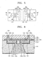
- FIG. 5 is an enlarged plan view of a portion A of FIG. 4
- FIG. 6 is a cross-sectional view illustrating a vertical structure of the ink-jet printhead taken along line VI-VI' of FIG. 5
- FIG. 7 is a partial perspective view of a substrate illustrating an ink chamber and an ink passage, which are formed on the surface of the substrate.
- an ink chamber 106 to be filled with ink is formed on the surface of a substrate 100 to a predetermined depth, and a manifold 102 which supplies ink to the ink chamber 106 is formed on a rear surface of the substrate 100.
- the ink chamber 106 and the manifold 102 may have a variety of shapes.
- the ink chamber 106 may be formed to a depth of about 10-80 ⁇ m.
- the manifold 102 formed under the ink chamber 106 is connected to an ink reservoir (not shown).
- An ink passage 105 which connects the ink chamber 106 and the manifold 102 is formed on the surface of the substrate 100.
- the surface of the substrate 100 is etched to form the ink passage 105.
- the ink passage 105 may have a variety of shapes.
- the ink passage 105 is formed parallel to the surface of the substrate 100, in the same plane as the ink chamber 106.
- the ink passage 105 comprises an ink channel 105a and an ink feed hole 105b.
- the ink channel 105a is connected to the ink chamber 106, and the ink feed hole 105b is connected to the manifold 102.
- a plurality of ink channels 105a may be formed in consideration of an ejection property.
- a nozzle plate 120 is disposed on the substrate 100 on which the ink chamber 106, the ink passage 105, and the manifold 102 are formed.
- the nozzle plate 120 forms an upper wall of the ink chamber 106 and the ink passage 105.
- a nozzle 104 through which ink is ejected from the ink chamber 106 is vertically formed through the nozzle plate 120.
- the nozzle plate 120 is formed of a plurality of material layers stacked on the substrate 100.
- the plurality of material layers includes first, second, and third passivation layers 121, 122, and 126, and a heat dissipation layer 128 formed of metal.
- a heater 108 is disposed between the first passivation layer 121 and the second passivation layer 122, and a conductor (112 of FIG. 5 ) is disposed between the second passivation layer 122 and the third passivation layer 126.
- the first passivation layer 121 is a lowermost material layer of the plurality of material layers which are components of the nozzle plate 120, and is formed on the surface of the substrate 100.
- the first passivation layer 121 is formed to provide insulation between the heater 108 and the substrate 100 and to protect the heater 122.
- the first passivation layer 121 may be formed of silicon oxide or silicon nitride.
- the heater 108 which heats ink in the ink chamber 106 is disposed on the first passivation layer 121 formed on the ink chamber 106.
- a plurality of heaters 108 may be formed and may have a variety of positions and shapes, which are different from those shown in FIGS. 5, 6 , and 7 .
- the heater 108 may be formed in a ring shape around the nozzle 104.
- the heater 108 is formed of a resistive heating material, such as impurity-doped poly silicon, tantalum-aluminum alloy, tantalum nitride, titanium nitride, or tungsten silicide.
- the second passivation layer 122 is formed on the first passivation layer 121 and the heater 108.
- the second passivation layer 122 is formed to protect the heater 108 and may be formed of silicon nitride or silicon oxide, like the first passivation layer 121.
- a conductor (112 of FIG. 5 ) which is electrically connected to the heater 108 and applies a pulse current to the heater 108 is formed on the second passivation layer 122.
- One end of the conductor (112 of FIG. 5 ) is connected to the heater 108 via a contact hole formed in the second passivation layer 122, and the other end thereof is electrically connected to a bonding pad (101 of FIG. 4 ).
- the conductor (112 of FIG. 5 ) may be formed of metal with good conductivity, for example, aluminum (Al), aluminum alloy, gold (Au), or silver (Ag).
- the third passivation layer 126 is formed on the conductor (112 of FIG. 5 ) and the second passivation layer 122.
- the third passivation layer 126 may be formed of tetraethylorthosilicate (TEOS) oxide or silicon oxide.
- the heat dissipating layer 128, formed on the third passivation layer 126, is the uppermost material layer of the plurality of material layers which are components of the nozzle plate 120.
- the heat dissipating layer 128 may be formed of a metallic material with good thermal conductivity, such as Ni, Cu, Al, or Au.
- the heat dissipating layer 128 may be formed of a plurality of metallic layers.
- the heat dissipating layer 128 may be formed to a larger thickness of about 10 - 100 ⁇ m by electroplating the above-described metallic material.
- a seed layer 127 for electroplating of the above-described metallic material may be formed on the top surface of the third passivation layer 126 and at both sides of the surface of the substrate 100.
- the seed layer 127 may be formed of a metallic material with good electrical conductivity, such as Cu, Cr, Ti, Au, or Ni.
- the seed layer 127 may be formed of a plurality of metallic layers.
- the heat dissipating layer 128 dissipates heat generated by and remaining around the heater 108.
- heat generated by and remaining around the heater 108 after ink is ejected is dissipated to the substrate 100 and outside via the heat dissipating layer 128.
- heat is dissipated after ink is ejected and the temperature around the nozzle 104 falls rapidly so that printing can be performed stably at a high driving frequency.
- the nozzle 104 can be formed to have a sufficient length.
- a stable high-speed operation can be performed, and the linearity of ink droplets ejected through the nozzle 104 is improved. That is, the ink droplets can be ejected in a direction exactly perpendicular to the substrate 100.
- the nozzle 104 comprises a lower nozzle 104a and an upper nozzle 104b.
- the lower nozzle 104a has a cylindrical shape and is formed in the first, second, and third passaivation layers 121, 122, and 126.
- the upper nozzle 104b has a tapered shape such that a diameter thereof becomes smaller in the direction of an outlet in the heat dissipating layer 128. Since the upper nozzle 104 has a tapered shape, a meniscus at the surface of ink in the nozzle 104 is more quickly stabilized after ink is ejected.
- the ink chamber 106 is refilled with ink supplied from the manifold 102 through the ink channel 105a and the ink feed hole 105b.
- the above-described cycle is repeated.
- the ink passage 105 is formed parallel to the surface of the substrate 100 in the same plane as the ink chamber 106, backflow of ink can be reduced. Since the ink chamber 106 and the ink passage 105 are formed using an etching method, they may have a variety of shapes. Thus, the ink chamber 106 and the ink passage 105 can be formed to have optimum shapes. In addition, since the metal heat dissipating layer 128 is formed by electroplating, it may be formed as a single body with the other elements of the ink-jet printhead and formed to a larger thickness, and heat can be effectively dissipated.
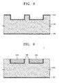
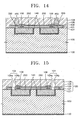
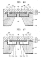
- FIGS. 8 through 19 are cross-sectional views illustrating a method for manufacturing an ink-jet printhead according to an embodiment of the present invention.
- FIG. 8 illustrates a state in which a groove is formed on the surface of the substrate 100, and the substrate 100 is oxidized to form silicon oxide layers 130 and 140 on the front and rear surfaces of the substrate 100.
- a silicon wafer is processed to a thickness of about 300-700 ⁇ m and is used as the substrate 100.
- Silicon wafers are widely used to manufacture semiconductor devices, and thus are good for mass production of a printhead. While FIG. 8 illustrates only a part of a silicon wafer, several tens to hundreds of chips corresponding to ink-jet printheads maybe contained in one wafer.
- An etching mask for defining a portion to be etched is formed on a top surface of the silicon substrate 100.
- a photoresist is coated on the top surface of the substrate 100 to a predetermined thickness and is patterned, thereby forming the etch mask.
- the substrate 100 exposed by the etch mask is etched, thereby forming a groove having a predetermined shape.
- the substrate 100 may be etched by dry etching such as reactive ion etching (RIE).
- RIE reactive ion etching
- the groove is a portion in which an ink chamber (106 of FIG. 6 ) and an ink passage (105 of FIG. 6 ) are to be formed.
- the depth of the groove is about 10-80 ⁇ m.
- the groove may have a variety of shapes depending on the shape in which the surface of the substrate 100 is etched.
- the ink chamber and the ink passage can be formed to have desired shapes.
- the etch mask is removed from the substrate 100.
- the substrate 100 on which the grove is formed is oxidized to form the silicon oxide layers 130 and 140 on the front and rear surfaces of the substrate 100.
- FIG. 9 illustrates a state in which a sacrificial layer 250 is formed in the groove formed on the substrate 100 and the surface of the substrate 100 is planarized.
- poly silicon is epitaxially grown in the groove formed on the surface of the oxidized substrate 100, thereby forming the sacrificial layer 250.
- the sacrificial layer 250 and the surface of the substrate 100 are planarized by a chemical mechanical polishing (CMP) process.
- CMP chemical mechanical polishing
- FIG. 10 illustrates a state in which the first passivation layer 121, the heater 108, the second passivation layer 122, the conductor (112 of FIG. 5 ), and the third passivation layer 126 are sequentially stacked on the entire surface of the structure shown in FIG. 9 .
- the first passivation layer 121 is formed on the surface of the planarized substrate 100.
- the first passivation layer 121 may be formed by depositing silicon oxide or silicon nitride.
- the heater 108 is formed on the first passivation layer 121.
- the heater 108 is formed by depositing a resistive heating material, such as impurity-doped poly silicon, tantalum-aluminum alloy, tantalum nitride, or tungsten silicide, on the entire surface of the first passivation layer 121 to a predetermined thickness and patterning the deposited material in a predetermined shape.
- impurity-doped poly silicon may be formed to a thickness of about 0.7-1 ⁇ m by depositing poly silicon together with impurities, for example, a source gas of phosphorous (P), by low pressure chemical vapor deposition (LP CVD).
- the heater 108 When the heater 108 is formed of tantalum-aluminum alloy, tantalum nitride, or tungsten silicide, the heater 108 may be formed to a thickness of about 0.1-0.3 ⁇ m by depositing tantalum-aluminum alloy, tantalum nitride, or tungsten silicide by sputtering or chemical vapor deposition (CVD). The deposition thickness of the resistive heating material may be varied so as to have proper resistance in consideration of the width and length of the heater 108.
- the resistive heating material deposited on the entire surface of the first passivation layer 121 is patterned by a photolithographic process using a photomask and a photoresist and an etch process using a photoresist pattern as an etch mask.
- the second passivation layer 122 formed of silicon oxide or silicon nitride may be formed to a thickness of about 0.2-1 ⁇ m by depositing silicon oxide or silicon nitride on the entire surface of the first passivation layer 121 on which the heater 108 is formed. Subsequently, the second passivation layer 122 is etched to form a contact hole (not shown) through which the heater 108 is exposed to be connected to the conductor (112 of FIG. 5 ).
- the conductor (112 of FIG. 5 ) is formed by depositing metal having good conductivity, such as aluminum (Al), aluminum alloy, gold (Au), or silver (Ag), on the entire surface of the second passivation layer 122 to a thickness of about 0.5-2 ⁇ m through sputtering and patterning the deposited metal. Then, the conductor (112 of FIG. 5 ) is connected to the heater 108 via the contact hole (not shown).
- metal having good conductivity such as aluminum (Al), aluminum alloy, gold (Au), or silver (Ag)
- the third passivation layer 126 is formed on top surfaces of the second passivation layer 122 and the conductor (112 of FIG. 5 ).
- the third passivation layer 126 is a material layer that provides insulation between the conductor (112 of FIG. 5 ) and a heat dissipating layer (128 of FIG. 6 ) that will be formed later.
- the third passivation layer 126 may be formed to a thickness of about 0.7-3 ⁇ m by depositing TEOS oxide using plasma enhanced chemical vapor deposition (PE CVD).
- FIG. 11 illustrates a state in which the lower nozzle 104a is formed.
- the lower nozzle 104a may be formed by sequentially etching the third passivation layer 126, the second passivation layer 122, and the first passivation layer 121 through RIE such that part of the sacrificial layer 250 formed on the surface of the substrate 100 and both sides of the surface of the substrate 100 is exposed.
- FIG. 12 illustrates a state in which a lower plating mold 350 is formed in the lower nozzle 104a and the seed layer 127 is formed on the lower plating mold 350.
- the lower plating mold 350 may be formed by coating a photoresist on the entire surface of the structure shown in FIG. 11 to a predetermined thickness, patterning a coated photoresist, and leaving only the photoresist inside the lower nozzle 104a.
- the lower plating mold 350 may be formed of a photoresist or a photosensitive polymer.
- the seed layer 127 for electroplating is formed on the entire surface of the structure shown in FIG. 12 .
- the seed layer 127 may be formed to a thickness of about 500-3000 A by depositing metal having good conductivity, such as Cu, Cr, Ti, Au, or Ni, by sputtering.
- the seed layer 127 may be formed of a plurality of metallic layers.
- FIG. 13 illustrates a state in which an upper plating mold 450 for forming an upper nozzle (104b of FIG. 6 ) is formed.
- the upper plating mold 450 may be formed by coating a photoresist on the entire surface of the seed layer 127, patterning the coated photoresist, and leaving only photoresist where the upper nozzle (104b of FIG. 6 ) is to be formed. Meanwhile, the upper plating mold 450 may be formed of a photoresist or photosensitive polymer.
- the upper plating mold 450 has a tapered shape such that a diameter thereof becomes smaller as the upper plating mold 450 extends upwards.
- the upper nozzle (104b of FIG. 6 ) may have a cylindrical shape. In this case, the upper plating mold 450 may have the pillar shape.
- the lower plating mold 350 and the upper plating mold 450 may be formed by the following steps. Referring to FIG. 19 , before forming the lower plating mold 350, a seed layer 127' for electroplating is formed on the entire surface of the structure shown in FIG. 11 . Subsequently, the lower plating mold 350 and the upper plating mold 450 are sequentially formed. Alternatively, the lower and upper plating molds 350 and 450 may be formed of a single body.
- FIG. 14 illustrates a state in which the heat dissipating layer 128 formed of a metallic material having a predetermined thickness is formed on a top surface of the seed layer 127.
- the heat dissipating layer 128 may be formed to a thickness of about 10-100 ⁇ m by electroplating metal having good thermal conductivity, such as Ni, Cu, Al, or Au, on the surface of the seed layer 127.
- the heat dissipating layer 128 may be formed of a plurality of metallic layers.
- the thickness of the heat dissipating layer 128 may be determined in consideration of a cross-sectional area and shape of the upper nozzle and a heat dissipating capability to the substrate 100 and the outside.
- the surface of the heat dissipating layer 128 after electroplating is completed is uneven due to material layers formed under the heat dissipating layer 128.
- the surface of the heat dissipating layer 128 can be planarized by CMP.
- the upper plating mold 450, the seed layer 127 formed under the upper plating mold 450, and the lower plating mold 350 are sequentially removed.
- the upper and lower plating molds 450 and 350 may be removed using a general method of removing a photoresist.
- the seed layer 127 may be etched by wet etching using an etchant capable of selectively etching the seed layer 127 in consideration of etch selectivity of the metallic material used to form the heat dissipating layer 128 to the metallic material used to form the seed layer 127.
- the seed layer 127 is formed of copper (Cu)
- an acetic acid based etchant may be used
- a HF based etchant may be used.
- the lower nozzle 104a and the upper nozzle 104b are connected to each other, thereby forming a complete nozzle 104 and completing the nozzle plate 120 formed of a stack of a plurality of material layers.
- a partial surface of the sacrificial layer 250 that occupies a space in which the ink chamber (106 of FIG. 6 ) and the ink passage (105 of FIG. 6 ) are to be formed, is exposed through the nozzle 104.
- FIG. 16 illustrates a state in which the manifold 102 is formed on a rear surface of the substrate 100.
- the silicon oxide layer 130 formed on the rear surface of the silicon substrate 100 is patterned, thereby forming an etch mask which defines an area to be patterned.
- the silicon substrate 100 exposed by the etch mask is wet etched using tetramethyl ammonium hydroxide (TMAH) or potassium hydroxide (KOH) as an etchant, thereby forming the manifold 102 having an inclined side, as shown in FIG. 16 .
- TMAH tetramethyl ammonium hydroxide
- KOH potassium hydroxide
- the manifold 102 may be formed by anisotropically dry etching the rear surface of the substrate 100.
- FIG. 17 illustrates a state in which the ink chamber 106 and the ink passage 105 are formed on the surface of the substrate 100.
- the ink chamber 106 and the ink passage 105 may be formed by isotropically etching the sacrificial layer (250 of FIG. 16 ).
- the sacrificial layer (250 of FIG. 16 ) exposed through the nozzle 104 is dry etched using an etchant, such as an XeF 2 gas or a BrF 3 gas, for a predetermined amount of time.
- an etchant such as an XeF 2 gas or a BrF 3 gas
- the ink chamber 106 and the ink passage 105 are formed parallel to the surface of the substrate 100 in the same plane.
- the depths of the ink chamber 106 and the ink passage 105 formed on the surface of the substrate 100 are about 10-80 ⁇ m.
- the ink passage 105 includes an ink channel 105a connected to the ink chamber 106 and an ink feed hole 105b connected to the manifold 102.
- FIG. 18 illustrates a state in which the ink passage 105 and the manifold 102, which are formed on the substrate 100, are connected to each other. Specifically, the silicon oxide layer 140 between the ink passage 105 formed on the front surface of the substrate 100 and the manifold 102 formed on the rear surface of the substrate 100 is removed by etching, thereby connecting the ink passage 105 to the manifold 102.
- the ink-jet printhead according to the embodiment of the present invention is now complete.
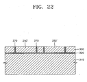
- FIGS. 20 through 22 are cross-sectional views illustrating a method for manufacturing an ink-jet printhead according to another embodiment of the present invention. This method is the same as the method of the previous embodiment, except for the step of forming the sacrificial layer, and thus, only the step of forming the sacrificial layer will be described.
- a silicon-on-insulator (SOI) substrate 300 in which an insulating layer 320 is interposed between two silicon substrates 310 and 330, is used as a substrate.
- the thickness of the upper silicon substrate 330 is about 10-80 ⁇ m
- the thickness of the lower silicon substrate 310 is about 300-700 ⁇ m.
- the surface of the upper silicon substrate 330 is etched, thereby forming a trench 340 having a predetermined shape so that the insulating layer 320 is exposed.
- the trench 340 is formed to surround portions in which the ink chamber (106 of FIG. 6 ) and the ink passage (105 of FIG. 6 ) are to be formed.
- the trench 340 is formed to a width of several ⁇ m so that it can easily be filled with a predetermined material.
- the trench 340 is filled with a silicon oxide 370, and then, the surface of the upper silicon substrate 330 is planarized. By doing so, portions that are surrounded by the silicon oxide 370 become sacrificial layers 250' for forming the ink chamber (106 of FIG. 6 ) and the ink passage (105 of FIG. 6 ).
- the sacrificial layer 250' is formed of silicon, unlike in the previous embodiment in which it was formed of poly silicon.
- the ink-jet printhead and the method for manufacturing the same according to the present invention have the following effects.
- heat generated by and remaining around a heater is efficiently dissipated to the substrate and outside. Thus, the area near the nozzle can be rapidly cooled enabling a driving frequency to be increased.
Landscapes
- Engineering & Computer Science (AREA)
- Manufacturing & Machinery (AREA)
- Particle Formation And Scattering Control In Inkjet Printers (AREA)
Claims (24)
- Tête d'impression à jet d'encre comprenant :un substrat (100), une chambre d'encrage (106) à remplir d'encre devant être éjectée, formée sur une surface du substrat (100), un collecteur (102) qui fournit de l'encre à la chambre d'encrage (106), formé sur une surface arrière du substrat (100), et un conduit d'encre (105) qui relie la chambre d'encrage (106) et le collecteur (102), formé parallèlement à la surface du substrat (100) et dans le même plan que la chambre d'encrage (106) ;une plaque à buse (120), qui comprend une pluralité de couches de passivation (121, 122, 126) empilées sur le substrat (100) et formées d'un matériau isolant, à travers laquelle une buse (104) reliée à la chambre d'encrage (106) est formée ; etun dispositif de chauffage (108) et un conducteur (112), qui sont disposés entre les couches de passivation (121, 122, 126) de la plaque à buse (120), le dispositif de chauffage (108) étant positionné sur la chambre d'encrage (106) et chauffant l'encre dans la chambre d'encrage (106), et le conducteur (112) appliquant un courant au dispositif de chauffage (108),dans laquelle la tête d'impression à jet d'encre est caractérisée en ce que la plaque à buse (120) comprend en outre une couche de dissipation thermique (128) formée sur les couches de passivation (121, 122, 126), la couche de dissipation thermique (128) étant formée d'un matériau métallique ayant une bonne conductibilité thermique.
- Tête d'impression à jet d'encre selon la revendication 1, dans laquelle le conduit d'encre (105) comprend au moins un canal d'encre (105a) relié à la chambre d'encrage (106) et un orifice d'alimentation d'encre (105b) qui relie le canal d'encre (105a) au collecteur (102).
- Tête d'impression à jet d'encre selon l'une quelconque des revendications précédentes, dans laquelle les couches de passivation comprennent une première couche de passivation (121), une deuxième couche de passivation (122) et une troisième couche de passivation (126), qui sont empilées de manière séquentielle sur le substrat (100), dans laquelle le dispositif de chauffage (108) est disposé entre la première couche de passivation (121) et la deuxième couche de passivation (122), et dans laquelle le conducteur (112) est disposé entre la deuxième couche de passivation (122) et la troisième couche de passivation (126).
- Tête d'impression à jet d'encre selon l'une quelconque des revendications précédentes, dans laquelle une partie inférieure de la buse (104a) est formée dans la pluralité des couches de passivation (121, 122, 126), et dans laquelle une partie supérieure de la buse (104b) est formée dans la couche de dissipation thermique (128).
- Tête d'impression à jet d'encre selon la revendication 4, dans laquelle la partie supérieure de la buse (104b) formée dans la couche de dissipation thermique (128) a une forme effilée de telle sorte que le diamètre de celle-ci devienne plus petit dans la direction d'une sortie.
- Tête d'impression à jet d'encre selon l'une quelconque des revendications précédentes, dans laquelle la couche de dissipation thermique (128) est formée d'au moins une couche métallique, et dans laquelle chacune des couches métalliques est formée d'au moins un matériau sélectionné parmi le groupe se composant de Ni, Cu, Al et Au.
- Tête d'impression à jet d'encre selon l'une quelconque des revendications précédentes, dans laquelle la couche de dissipation thermique (128) est formée par galvanoplastie avec une épaisseur d'environ 10 à 100 µm.
- Tête d'impression à jet d'encre selon l'une quelconque des revendications précédentes, dans laquelle une couche d'ensemencement (127) destinée à galvaniser la couche de dissipation thermique est formée sur les couches de passivation.
- Tête d'impression à jet d'encre selon la revendication 8, dans laquelle la couche d'ensemencement (127) est formée d'au moins une couche métallique, et dans laquelle chacune des couches métalliques est formée d'au moins un matériau sélectionné parmi le groupe se composant de Cu, Cr, Ti, Au et Ni.
- Procédé de fabrication d'une tête d'impression à jet d'encre, le procédé comprenant :la formation sur une surface du substrat (100) d'une couche sacrificielle (250) ayant une profondeur prédéterminée ;l'empilement de manière séquentielle d'une pluralité de couches de passivation (121, 122, 126) sur le substrat (100) sur lequel la couche sacrificielle (250) est formée, et la formation d'un dispositif de chauffage (108) et d'un conducteur (112) relié au dispositif de chauffage entre les couches de passivation (121, 122, 126) ;la formation d'une couche de dissipation thermique en métal (128) sur les couches de passivation (121, 122, 126) et la formation d'une buse (104) par laquelle l'encre est éjectée à travers la couche de dissipation thermique (128) et les couches de passivation (121, 122, 126) pour exposer la couche sacrificielle (250) ;la formation d'un collecteur (102) destiné à fournir de l'encre sur une surface arrière du substrat (100) ;le retrait de la couche sacrificielle (250) pour former une chambre d'encrage (106) et un conduit d'encre (105), le conduit d'encre (105) étant formé parallèlement à la surface du substrat (100) et dans le même plan que la chambre d'encrage (106) ; etla liaison du collecteur (102) au conduit d'encre (105).
- Procédé selon la revendication 10, dans lequel la formation de la couche sacrificielle (250) comprend :le gravage de la surface du substrat (100) pour former une rainure ayant une profondeur prédéterminée ;l'oxydation de la surface du substrat (100) dans laquelle la rainure est formée pour former une couche d'oxyde (140) ; etle remplissage de la rainure avec un matériau prédéterminé (250) et la planarisation de la surface du substrat (100).
- Procédé selon la revendication 11, dans lequel le remplissage de la rainure avec le matériau prédéterminé (250) est effectué en faisant croître par épitaxie du polysilicium dans la rainure.
- Procédé selon la revendication 10, dans lequel la formation de la couche sacrificielle (250') comprend :la formation d'une tranchée (340) exposant une couche isolante (320) dans une forme prédéterminée dans un substrat supérieur en silicium (330) d'un substrat en silicium sur isolant (300) ; etle remplissage de la tranchée (340) avec un matériau prédéterminé (370).
- Procédé selon la revendication 13, dans lequel le matériau prédéterminé (370) est de l'oxyde de silicium.
- Procédé selon l'une quelconque des revendications 10 à 14, dans lequel la formation des couches de passivation (121, 122, 126) comprend :la formation d'une première couche de passivation (121) sur la surface du substrat (100) sur laquelle la couche sacrificielle (250) est formée ;la formation du dispositif de chauffage (108) sur la première couche de passivation (121) ;la formation d'une deuxième couche de passivation (122) sur la première couche de passivation (121) et le dispositif de chauffage (108) ;la formation du conducteur (112) sur la deuxième couche de passivation (122) ; etla formation d'une troisième couche de passivation (126) sur la deuxième couche de passivation (122) et le conducteur (112).
- Procédé selon l'une quelconque des revendications 10 à 15, dans lequel la couche de dissipation thermique (128) est formée d'au moins une couche métallique, et dans lequel chacune des couches métalliques est formée en galvanisant au moins un matériau sélectionné parmi le groupe se composant de Ni, Cu, Al et Au.
- Procédé selon l'une quelconque des revendications 10 à 16, dans lequel la couche de dissipation thermique (128) est formée avec une épaisseur de 10 à 100 µm.
- Procédé selon l'une quelconque des revendications 10 à 17, dans lequel la formation de la couche de dissipation thermique (128) et de la buse (104) comprend :Le gravage des couches de passivation (121, 122, 126) formées sur la couche sacrificielle (250) pour former une buse inférieure (104a) ;la formation d'un moule de placage inférieur (350) à l'intérieur de la buse inférieure (104a) ;la formation d'un moule de placage supérieur (450) ayant une forme prédéterminée destiné à former la buse supérieure (104b) sur le moule de placage inférieur (350) ;la formation de la couche de dissipation thermique (128) sur les couches de passivation (121, 122, 126) par galvanoplastie ; etle retrait des moules de placage supérieur et inférieur (350, 450) pour former la buse (104) comprenant la buse supérieure (104b) et la buse inférieure (104a).
- Procédé selon l'une quelconque des revendications 10 à 17, dans lequel la formation de la couche de dissipation thermique (128) et de la buse (104) comprend :le gravage des couches de passivation (121, 122, 126) formées sur la couche sacrificielle (250) pour former une buse inférieure (104a) ;la formation d'un moule de placage (450) ayant une forme prédéterminée destiné à former une buse supérieure verticalement à partir de l'intérieur de la buse inférieure ;la formation de la couche de dissipation thermique (128) sur les couches de passivation (121, 122, 126) par galvanoplastie ; etle retrait du moule de placage (450) et la formation de la buse (104) comprenant la buse supérieure (104b) et la buse inférieure (104a).
- Procédé selon la revendication 18 ou 19, dans lequel le ou les moules de placage (350, 450) est/sont formé(s) d'un polymère photorésistant ou photosensible.
- Procédé selon l'une quelconque des revendications 18 à 20, dans lequel la buse inférieure (104a) est formée par gravure sèche des couches de passivation (121, 122, 126) par gravage ionique réactif.
- Procédé selon l'une quelconque des revendications 18 à 21, dans lequel la formation de la couche de dissipation thermique (128) et de la buse (104) comprend en outre la formation d'une couche d'ensemencement (127) destinée à galvaniser la couche de dissipation thermique (128) sur les couches de passivation (121, 122, 126).
- Procédé selon la revendication 22, dans lequel la couche d'ensemencement (127) est formée d'au moins une couche métallique, et dans lequel chacune des couches métalliques est formée en déposant au moins un matériau métallique sélectionné parmi le groupe se composant de Cu, Cr, Ti, Au et Ni.
- Procédé selon l'une quelconque des revendications 18 à 23, comprenant en outre, après la formation de la couche de dissipation thermique (128), la formation de la couche de dissipation thermique (128) et de la buse (104), la planarisation de la surface supérieure de la couche de dissipation thermique (128) grâce à un procédé de polissage chimico-mécanique.
Applications Claiming Priority (2)
| Application Number | Priority Date | Filing Date | Title |
|---|---|---|---|
| KR2003033840 | 2003-05-27 | ||
| KR1020030033840A KR100590527B1 (ko) | 2003-05-27 | 2003-05-27 | 잉크젯 프린트헤드 및 그 제조방법 |
Publications (2)
| Publication Number | Publication Date |
|---|---|
| EP1481806A1 EP1481806A1 (fr) | 2004-12-01 |
| EP1481806B1 true EP1481806B1 (fr) | 2008-07-09 |
Family
ID=33129041
Family Applications (1)
| Application Number | Title | Priority Date | Filing Date |
|---|---|---|---|
| EP04253091A Expired - Lifetime EP1481806B1 (fr) | 2003-05-27 | 2004-05-26 | Tête d'impression à jet d'encre et sa méthode de fabrication |
Country Status (4)
| Country | Link |
|---|---|
| EP (1) | EP1481806B1 (fr) |
| JP (1) | JP2004351931A (fr) |
| KR (1) | KR100590527B1 (fr) |
| DE (1) | DE602004014845D1 (fr) |
Families Citing this family (9)
| Publication number | Priority date | Publication date | Assignee | Title |
|---|---|---|---|---|
| KR100499150B1 (ko) | 2003-07-29 | 2005-07-04 | 삼성전자주식회사 | 잉크젯 프린트헤드 및 그 제조방법 |
| CN100389960C (zh) * | 2005-06-01 | 2008-05-28 | 明基电通股份有限公司 | 流体喷射装置的制造方法 |
| KR100644705B1 (ko) * | 2005-07-04 | 2006-11-10 | 삼성전자주식회사 | 잉크젯 프린트헤드 및 그 제조방법 |
| KR100723428B1 (ko) * | 2006-05-30 | 2007-05-30 | 삼성전자주식회사 | 잉크젯 프린트헤드 및 그 제조방법 |
| WO2008029650A1 (fr) * | 2006-09-08 | 2008-03-13 | Canon Kabushiki Kaisha | Tête d'éjection de liquide et son procédé de fabrication |
| US8562845B2 (en) * | 2006-10-12 | 2013-10-22 | Canon Kabushiki Kaisha | Ink jet print head and method of manufacturing ink jet print head |
| JP2008307828A (ja) | 2007-06-15 | 2008-12-25 | Canon Inc | 記録ヘッド |
| JP5038054B2 (ja) * | 2007-08-08 | 2012-10-03 | キヤノン株式会社 | 液体吐出ヘッドおよびその製造方法 |
| KR20240017214A (ko) | 2022-07-28 | 2024-02-07 | 삼성디스플레이 주식회사 | 표시 장치 및 그 제조방법 |
Family Cites Families (7)
| Publication number | Priority date | Publication date | Assignee | Title |
|---|---|---|---|---|
| AU657720B2 (en) | 1991-01-30 | 1995-03-23 | Canon Kabushiki Kaisha | A bubblejet image reproducing apparatus |
| US6019457A (en) * | 1991-01-30 | 2000-02-01 | Canon Information Systems Research Australia Pty Ltd. | Ink jet print device and print head or print apparatus using the same |
| DE4214555C2 (de) | 1992-04-28 | 1996-04-25 | Eastman Kodak Co | Elektrothermischer Tintendruckkopf |
| US6382782B1 (en) | 2000-12-29 | 2002-05-07 | Eastman Kodak Company | CMOS/MEMS integrated ink jet print head with oxide based lateral flow nozzle architecture and method of forming same |
| KR100668294B1 (ko) * | 2001-01-08 | 2007-01-12 | 삼성전자주식회사 | 반구형 잉크 챔버를 가진 잉크 젯 프린트 헤드 및 그제조방법 |
| TW510858B (en) * | 2001-11-08 | 2002-11-21 | Benq Corp | Fluid injection head structure and method thereof |
| KR100493160B1 (ko) * | 2002-10-21 | 2005-06-02 | 삼성전자주식회사 | 테이퍼 형상의 노즐을 가진 일체형 잉크젯 프린트헤드 및그 제조방법 |
-
2003
- 2003-05-27 KR KR1020030033840A patent/KR100590527B1/ko not_active Expired - Fee Related
-
2004
- 2004-05-14 JP JP2004145605A patent/JP2004351931A/ja active Pending
- 2004-05-26 DE DE602004014845T patent/DE602004014845D1/de not_active Expired - Lifetime
- 2004-05-26 EP EP04253091A patent/EP1481806B1/fr not_active Expired - Lifetime
Also Published As
| Publication number | Publication date |
|---|---|
| KR20040101862A (ko) | 2004-12-03 |
| DE602004014845D1 (de) | 2008-08-21 |
| KR100590527B1 (ko) | 2006-06-15 |
| EP1481806A1 (fr) | 2004-12-01 |
| JP2004351931A (ja) | 2004-12-16 |
Similar Documents
| Publication | Publication Date | Title |
|---|---|---|
| US7018017B2 (en) | Monolithic ink-jet printhead having a heater disposed between dual ink chambers and method for manufacturing the same | |
| US7368063B2 (en) | Method for manufacturing ink-jet printhead | |
| KR100493160B1 (ko) | 테이퍼 형상의 노즐을 가진 일체형 잉크젯 프린트헤드 및그 제조방법 | |
| US7334335B2 (en) | Method of manufacturing a monolithic ink-jet printhead | |
| EP1481806B1 (fr) | Tête d'impression à jet d'encre et sa méthode de fabrication | |
| EP1407883B1 (fr) | Tête d'impression à jet d'encre monolithique avec resevoir d'encre delimité par un parois de barrière et mèthode de fabrication associé | |
| EP1447223B1 (fr) | Tête d' impression à jet d' encre et sa méthode de fabrication | |
| EP1407884B1 (fr) | Tête d'impression par jet d'encre monolithe à plaque à orifices métallique et son procédé de fabrication | |
| EP1413439B1 (fr) | Tête d'impression à jet d'encre et sa méthode de fabrication | |
| EP1447222B1 (fr) | Tête à jet d'encre | |
| KR100499150B1 (ko) | 잉크젯 프린트헤드 및 그 제조방법 |
Legal Events
| Date | Code | Title | Description |
|---|---|---|---|
| PUAI | Public reference made under article 153(3) epc to a published international application that has entered the european phase |
Free format text: ORIGINAL CODE: 0009012 |
|
| AK | Designated contracting states |
Kind code of ref document: A1 Designated state(s): AT BE BG CH CY CZ DE DK EE ES FI FR GB GR HU IE IT LI LU MC NL PL PT RO SE SI SK TR |
|
| AX | Request for extension of the european patent |
Extension state: AL HR LT LV MK |
|
| 17P | Request for examination filed |
Effective date: 20050202 |
|
| AKX | Designation fees paid |
Designated state(s): DE FR GB |
|
| GRAP | Despatch of communication of intention to grant a patent |
Free format text: ORIGINAL CODE: EPIDOSNIGR1 |
|
| GRAS | Grant fee paid |
Free format text: ORIGINAL CODE: EPIDOSNIGR3 |
|
| RIN1 | Information on inventor provided before grant (corrected) |
Inventor name: BAEK, SEOG-SOON Inventor name: OH, YONG-SOO Inventor name: LIM, HYUNG-TAEK Inventor name: SHIN, JONG-WOO Inventor name: KIM, MIN-SOO Inventor name: SHIN, SU-HO |
|
| GRAA | (expected) grant |
Free format text: ORIGINAL CODE: 0009210 |
|
| AK | Designated contracting states |
Kind code of ref document: B1 Designated state(s): DE FR GB |
|
| REG | Reference to a national code |
Ref country code: GB Ref legal event code: FG4D |
|
| REF | Corresponds to: |
Ref document number: 602004014845 Country of ref document: DE Date of ref document: 20080821 Kind code of ref document: P |
|
| PLBE | No opposition filed within time limit |
Free format text: ORIGINAL CODE: 0009261 |
|
| STAA | Information on the status of an ep patent application or granted ep patent |
Free format text: STATUS: NO OPPOSITION FILED WITHIN TIME LIMIT |
|
| 26N | No opposition filed |
Effective date: 20090414 |
|
| REG | Reference to a national code |
Ref country code: FR Ref legal event code: PLFP Year of fee payment: 13 |
|
| REG | Reference to a national code |
Ref country code: GB Ref legal event code: 732E Free format text: REGISTERED BETWEEN 20170406 AND 20170412 |
|
| REG | Reference to a national code |
Ref country code: FR Ref legal event code: PLFP Year of fee payment: 14 |
|
| REG | Reference to a national code |
Ref country code: DE Ref legal event code: R082 Ref document number: 602004014845 Country of ref document: DE Representative=s name: PATENTANWAELTE RUFF, WILHELM, BEIER, DAUSTER &, DE Ref country code: DE Ref legal event code: R081 Ref document number: 602004014845 Country of ref document: DE Owner name: HP PRINTING KOREA CO., LTD., SUWON-SI, KR Free format text: FORMER OWNER: SAMSUNG ELECTRONICS CO., LTD., SUWON-SI, GYEONGGI-DO, KR Ref country code: DE Ref legal event code: R081 Ref document number: 602004014845 Country of ref document: DE Owner name: HEWLETT-PACKARD DEVELOPMENT COMPANY, L.P., SPR, US Free format text: FORMER OWNER: SAMSUNG ELECTRONICS CO., LTD., SUWON-SI, GYEONGGI-DO, KR Ref country code: DE Ref legal event code: R081 Ref document number: 602004014845 Country of ref document: DE Owner name: S-PRINTING SOLUTION CO., LTD., SUWON-SI, KR Free format text: FORMER OWNER: SAMSUNG ELECTRONICS CO., LTD., SUWON-SI, GYEONGGI-DO, KR |
|
| REG | Reference to a national code |
Ref country code: FR Ref legal event code: TP Owner name: S-PRINTING SOLUTION CO., LTD., KR Effective date: 20170912 |
|
| REG | Reference to a national code |
Ref country code: FR Ref legal event code: PLFP Year of fee payment: 15 |
|
| PGFP | Annual fee paid to national office [announced via postgrant information from national office to epo] |
Ref country code: DE Payment date: 20180419 Year of fee payment: 15 |
|
| PGFP | Annual fee paid to national office [announced via postgrant information from national office to epo] |
Ref country code: FR Payment date: 20180423 Year of fee payment: 15 |
|
| PGFP | Annual fee paid to national office [announced via postgrant information from national office to epo] |
Ref country code: GB Payment date: 20180419 Year of fee payment: 15 |
|
| REG | Reference to a national code |
Ref country code: DE Ref legal event code: R082 Ref document number: 602004014845 Country of ref document: DE Ref country code: DE Ref legal event code: R081 Ref document number: 602004014845 Country of ref document: DE Owner name: HP PRINTING KOREA CO., LTD., SUWON-SI, KR Free format text: FORMER OWNER: S-PRINTING SOLUTION CO., LTD., SUWON-SI, GYEONGGI-DO, KR Ref country code: DE Ref legal event code: R081 Ref document number: 602004014845 Country of ref document: DE Owner name: HEWLETT-PACKARD DEVELOPMENT COMPANY, L.P., SPR, US Free format text: FORMER OWNER: S-PRINTING SOLUTION CO., LTD., SUWON-SI, GYEONGGI-DO, KR |
|
| REG | Reference to a national code |
Ref country code: DE Ref legal event code: R119 Ref document number: 602004014845 Country of ref document: DE |
|
| REG | Reference to a national code |
Ref country code: DE Ref legal event code: R081 Ref document number: 602004014845 Country of ref document: DE Owner name: HEWLETT-PACKARD DEVELOPMENT COMPANY, L.P., SPR, US Free format text: FORMER OWNER: HP PRINTING KOREA CO., LTD., SUWON-SI, GYEONGGI-DO, KR |
|
| REG | Reference to a national code |
Ref country code: GB Ref legal event code: 732E Free format text: REGISTERED BETWEEN 20191212 AND 20191218 |
|
| GBPC | Gb: european patent ceased through non-payment of renewal fee |
Effective date: 20190526 |
|
| PG25 | Lapsed in a contracting state [announced via postgrant information from national office to epo] |
Ref country code: DE Free format text: LAPSE BECAUSE OF NON-PAYMENT OF DUE FEES Effective date: 20191203 Ref country code: GB Free format text: LAPSE BECAUSE OF NON-PAYMENT OF DUE FEES Effective date: 20190526 |
|
| PG25 | Lapsed in a contracting state [announced via postgrant information from national office to epo] |
Ref country code: FR Free format text: LAPSE BECAUSE OF NON-PAYMENT OF DUE FEES Effective date: 20190531 |