EP1482367A2 - System und Methode zur Herstellung von Graustufen durch die Verwendung von räumlichen Lichtmodulatoren in einem maskenlosen Lithographiesystem - Google Patents
System und Methode zur Herstellung von Graustufen durch die Verwendung von räumlichen Lichtmodulatoren in einem maskenlosen Lithographiesystem Download PDFInfo
- Publication number
- EP1482367A2 EP1482367A2 EP20040012133 EP04012133A EP1482367A2 EP 1482367 A2 EP1482367 A2 EP 1482367A2 EP 20040012133 EP20040012133 EP 20040012133 EP 04012133 A EP04012133 A EP 04012133A EP 1482367 A2 EP1482367 A2 EP 1482367A2
- Authority
- EP
- European Patent Office
- Prior art keywords
- light
- slms
- active areas
- pattern
- areas
- Prior art date
- Legal status (The legal status is an assumption and is not a legal conclusion. Google has not performed a legal analysis and makes no representation as to the accuracy of the status listed.)
- Withdrawn
Links
- 238000001459 lithography Methods 0.000 title claims abstract description 24
- 238000004519 manufacturing process Methods 0.000 title claims description 9
- 238000000034 method Methods 0.000 claims abstract description 34
- 238000005286 illumination Methods 0.000 claims abstract description 30
- 230000003287 optical effect Effects 0.000 claims description 10
- 230000001965 increasing effect Effects 0.000 claims description 6
- 238000000059 patterning Methods 0.000 claims description 2
- 235000012431 wafers Nutrition 0.000 description 21
- 239000000758 substrate Substances 0.000 description 12
- 239000004065 semiconductor Substances 0.000 description 6
- 239000004973 liquid crystal related substance Substances 0.000 description 4
- 230000008569 process Effects 0.000 description 4
- 230000002596 correlated effect Effects 0.000 description 3
- 239000000203 mixture Substances 0.000 description 3
- 239000011521 glass Substances 0.000 description 2
- 238000003384 imaging method Methods 0.000 description 2
- 238000000206 photolithography Methods 0.000 description 2
- 238000000429 assembly Methods 0.000 description 1
- 230000000712 assembly Effects 0.000 description 1
- 230000015572 biosynthetic process Effects 0.000 description 1
- 238000004891 communication Methods 0.000 description 1
- 230000001276 controlling effect Effects 0.000 description 1
- 238000001816 cooling Methods 0.000 description 1
- 230000008878 coupling Effects 0.000 description 1
- 238000010168 coupling process Methods 0.000 description 1
- 238000005859 coupling reaction Methods 0.000 description 1
- 238000005516 engineering process Methods 0.000 description 1
- 230000002708 enhancing effect Effects 0.000 description 1
- 239000000835 fiber Substances 0.000 description 1
- 239000000463 material Substances 0.000 description 1
- 238000004806 packaging method and process Methods 0.000 description 1
- 230000002093 peripheral effect Effects 0.000 description 1
- 229920002120 photoresistant polymer Polymers 0.000 description 1
- 230000010287 polarization Effects 0.000 description 1
- 230000035484 reaction time Effects 0.000 description 1
- 230000009467 reduction Effects 0.000 description 1
- XLYOFNOQVPJJNP-UHFFFAOYSA-N water Substances O XLYOFNOQVPJJNP-UHFFFAOYSA-N 0.000 description 1
Images


Classifications
-
- G—PHYSICS
- G03—PHOTOGRAPHY; CINEMATOGRAPHY; ANALOGOUS TECHNIQUES USING WAVES OTHER THAN OPTICAL WAVES; ELECTROGRAPHY; HOLOGRAPHY
- G03F—PHOTOMECHANICAL PRODUCTION OF TEXTURED OR PATTERNED SURFACES, e.g. FOR PRINTING, FOR PROCESSING OF SEMICONDUCTOR DEVICES; MATERIALS THEREFOR; ORIGINALS THEREFOR; APPARATUS SPECIALLY ADAPTED THEREFOR
- G03F7/00—Photomechanical, e.g. photolithographic, production of textured or patterned surfaces, e.g. printing surfaces; Materials therefor, e.g. comprising photoresists; Apparatus specially adapted therefor
- G03F7/20—Exposure; Apparatus therefor
-
- G—PHYSICS
- G03—PHOTOGRAPHY; CINEMATOGRAPHY; ANALOGOUS TECHNIQUES USING WAVES OTHER THAN OPTICAL WAVES; ELECTROGRAPHY; HOLOGRAPHY
- G03F—PHOTOMECHANICAL PRODUCTION OF TEXTURED OR PATTERNED SURFACES, e.g. FOR PRINTING, FOR PROCESSING OF SEMICONDUCTOR DEVICES; MATERIALS THEREFOR; ORIGINALS THEREFOR; APPARATUS SPECIALLY ADAPTED THEREFOR
- G03F7/00—Photomechanical, e.g. photolithographic, production of textured or patterned surfaces, e.g. printing surfaces; Materials therefor, e.g. comprising photoresists; Apparatus specially adapted therefor
- G03F7/70—Microphotolithographic exposure; Apparatus therefor
- G03F7/70216—Mask projection systems
- G03F7/70283—Mask effects on the imaging process
- G03F7/70291—Addressable masks, e.g. spatial light modulators [SLMs], digital micro-mirror devices [DMDs] or liquid crystal display [LCD] patterning devices
Definitions
- lithography a wafer, which is disposed on a wafer stage, is exposed to an image projected onto the surface of the wafer by exposure optics located within a lithography apparatus. While exposure optics are used in the case of photolithography, a different type of exposure apparatus can be used depending on the particular application. For example, x-ray, ion, electron, or photon lithography each can require a different exposure apparatus, as is known to those skilled in the art. The particular example of photolithography is discussed here for illustrative purposes only.
- the projected image produces changes in the characteristics of a layer, for example photoresist, deposited on the surface of the wafer. These changes correspond to the features projected onto the wafer during exposure. Subsequent to exposure, the layer can be etched to produce a patterned layer. The pattern corresponds to those features projected onto the wafer during exposure. This patterned layer is then used to remove or further process exposed portions of underlying structural layers within the wafer, such as conductive, semiconductive, or insulative layers. This process is then repeated, together with other steps, until the desired features have been formed on the surface, or in various layers, of the wafer.
- a layer for example photoresist
- Step-and-scan technology works in conjunction with a projection optics system that has a narrow imaging slot. Rather than expose the entire wafer at one time, individual fields are scanned onto the wafer one at a time. This is accomplished by moving the wafer and reticle simultaneously such that the imaging slot is moved across the field during the scan. The wafer stage must then be asynchronously stepped between field exposures to allow multiple copies of the reticle pattern to be exposed over the wafer surface. In this manner, the quality of the image projected onto the wafer is maximized.
- the system typically has a lithographic chamber that is designed to contain an apparatus that performs the process of image formation on the semiconductor wafer.
- the chamber can be designed to have different gas mixtures and/or grades of vacuum depending on the wavelength of light being used.
- a reticle is positioned inside the chamber.
- a beam of light is passed from an illumination source (located outside the system) through an optical system, an image outline on the reticle, and a second optical system before interacting with a semiconductor wafer.
- a plurality of reticles is required to fabricate a device on the substrate. These reticles are becoming increasingly costly and time consuming to manufacture due to the feature sizes and the exacting tolerances required for small feature sizes. Also, a reticle can only be used for a certain period of time before being worn out. Further costs are routinely incurred if a reticle is not within a certain tolerance or when the reticle is damaged. Thus, the manufacture of wafers using reticles is becoming increasingly, and possibly prohibitively, expensive.
- the present invention provides a method for producing gray scale patterns on objects during maskless lithography.
- the method includes illuminating light onto an array of spatial light modulators (SLMs), patterning the light with the SLMs to produce an exposure light pattern having spatially varying intensities, and writing the patterned light onto the object to produce the gray scaled patterns on the object based on the spatially varying light intensities.
- SLMs spatial light modulators
- the present invention also provides a maskless lithography system for producing gray scale patterns on objects.
- the system includes an illumination source, an object including an array of exposure areas, an array of spatial light modulators, and a controller.
- the array of spatial light modulators pattern and direct light from the illumination source to the object.
- Each of the spatial light modulators have active areas that respectively correspond with one of the exposure areas on the object.
- the controller controls the array of spatial light modulators, such that the pattern of the light has spatially varying intensities.
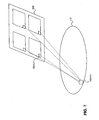
- FIG. 1 shows a maskless lithography system having reflective spatial light modulators according to embodiments of the present invention
- FIG. 3 shows a spatial light modulator according to an embodiment of the present invention.
- FIG. 4 shows more details of the spatial light modulator in FIG. 3.
- FIG. 8 shows a flow chart depicting a method 800 according to embodiments of the present invention.
- the present invention provides a maskless lithography system and method for producing gray scale patterns on objects.
- the system includes an illumination source (e.g., either pulsed or effectively continuous), an object including an array of exposure areas, an array of spatial light modulators (e.g., either digital, binary, or analog), and a controller.
- the array of spatial light modulators pattern and direct light from the illumination source to the object.
- Each of the spatial light modulators have active areas that respectively correspond with one of the exposure areas on the object.
- the controller controls the array of spatial light modulators, such that the pattern of the light has spatially varying intensities.
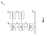
- FIG. 1 shows a maskless lithography system 100 according to an embodiment of the present invention.
- System 100 includes an illumination system 102 that transmits light to a reflective spatial light modulator 104 (e.g., a digital micromirror device (DMD), a reflective liquid crystal display (LCD), or the like) via a beam splitter 106 and SLM optics 108.
- SLM 104 is used to pattern the light in place of a reticle in traditional lithography systems. Patterned light reflected from SLM 104 is passed through beam splitter 106 and projection optics 110 and written on an object 112 (e.g., a substrate, a semiconductor wafer, a glass substrate for a flat panel display, or the like).
- object 112 e.g., a substrate, a semiconductor wafer, a glass substrate for a flat panel display, or the like.
- illumination optics can be housed within illumination system 102, as is known in the relevant art. It is also to be appreciated that SLM optics 108 and projection optics 110 can include any combination of optical elements required to direct light onto desired areas of SLM 104 and/or object 112, as is known in the relevant art.
- either one or both of illumination system 102 and SLM 104 can be coupled to or have integral controllers 114 and 116, respectively.
- Controller 114 can be used to adjust illumination source 102 based on feedback from system 100 or to perform calibration.
- Controller 116 can also be used for adjustment and/or calibration.
- controller 116 can be used for turning ON and OFF active devices 302 (e.g., pixels, mirrors, locations, etc.) (see FIG. 3) on SLM 104, as was described above, to generate a pattern used to expose object 112.
- Controller 116 can either have integral storage or be coupled to a storage element (not shown) with predetermined information and/or algorithms used to generate the pattern or patterns.
- FIG. 2 shows a maskless lithography system 200 according to a further embodiment of the present invention.
- System 200 includes an illumination source 202 that transmits light through a SLM 204 (e.g., a transmissive LCD, or the like) to pattern the light. The patterned light is transmitted through projection optics 210 to write the pattern on a surface of an object 212.
- SLM 204 is a transmissive SLM, such as a liquid crystal display, or the like.
- controllers 214 and 216 can perform similar functions as controller 114 and 116 described above, and as known in the art.
- Example SLMs that can be used in systems 100 or 200 are manufactured by Micronic Laser Systems AB of Sweden, Texas Instruments of Texas, USA, and Fraunhofer Institute for Circuits and Systems of Germany.
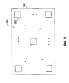
- FIG. 3 shows details of an active area 300 of SLM 104.
- Active area 300 includes an array of active devices 302 (represented by dotted patterns in the figure).
- Active devices 302 can be mirrors on a DMD or locations on a LCD. It is to be appreciated that active devices 302 can also be referred to as pixels, as is known in the relevant art.
- Digital or analog input signals based on a desired pattern are used to turn ON and OFF various active devices 302.
- an actual pattern being written to object 112 can be detected and a determination can be made whether the pattern is outside an acceptable tolerance. If so, controller 116 can be used to generate analog or digital control signals in real time to fine-tune (e.g., calibrate, adjust, etc.) the pattern being generated by SLM 104.
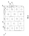
- FIG. 5 shows an assembly 500 including a support device 502 that receives an array of SLMs 104.
- the array of SLMs 104 can have varying numbers of columns, rows, SLMs per column, SLMs per row, etc., based on a number of desired exposures per pulse, or other criteria of a user.
- the SLMs 104 can be coupled to a support device 502.
- Support device 502 can have thermal control areas 504 (e.g., water or air channels, etc.), areas for control logic and related circuitry (e.g., see FIG.
- Support device 502 SLMs 104, and all peripheral cooling or control devices are referred to as an assembly.
- Assembly 500 can allow for a desired step size to produce the desired stitching (e.g., connecting of adjacent elements of features on object 112) and overlap for leading and trailing SLMs 104.
- support device 502 can be 250 mm x 250 mm (12 in x 12 in) or 300 mm x 300 mm (10 in x 10 in).
- Support device 502 can be used for thermal management based on being manufactured from a temperature stable material.
- Support device 502 can be utilized as a mechanical backbone to ensure spacing control of SLMs 104 and for embedding the circuitry and the thermal controls areas 504. Any electronics can be mounted on either or both of a backside and front side of support device 502. For example, when using analog based SLMs or electronics, wires can be coupled from control or coupling systems 504 to active areas 300. Based on being mounted on support device 502, these wires can be relatively shorter, which reduces attenuation of analog signals compared to a case where the circuitry is remote from the support device 502. Also, having short links between the circuitry and active areas 300 can increase communication speed, and thus increase pattern readjustment speed in real time.
- assembly 500 when SLM 104 or electrical devices in the circuitry wear out, assembly 500 can easily be replaced. Although it would appear replacing assembly 500 is more costly than just a chip on assembly 500, it is in fact easier and quicker to replace the entire assembly 500, which can save production costs. Also, assembly 500 can be refurbished, allowing for a reduction in replacement parts if end users are willing to use refurbished assemblies 500. Once assembly 500 is replaced, only an overall alignment is needed before resuming fabrication.
- the present invention provides for gray scaling of patterned areas on an object using a maskless lithography system.
- the gray scaling is based on using an array of spatial light modulators (SLMs).
- SLMs spatial light modulators
- Each exposure area on the object correlates to one active area on each of the SLMs.
- each exposure area is written to, or not written to as the case may be, by each SLM.
- a level of gray scaling is determined by the number of SLMs used in the array.
- An illumination system can include either a pulsed light source or an equivalent substantially continuous light source.
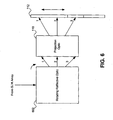
- FIG. 6 shows a portion 600 of either system 100 or 200 when a continuous light source is used.
- Portion 600 includes a rotating optical element 602 (e.g., a prism, or a circular, spherical, or conical optical reflecting element, or the like), which can rotate in any direction, positioned between SLMs 104 and projection optics 110.
- Arrows numbered 1, 2, and 3 show a possible light beam direction leaving rotating element 602 and, in turn, projection optic 110, based on a scanning position of object 112, as is discussed in more detail below.
- This system can use either a digital SLM or an analog SLM, which is discussed below.
- FIG. 7 shows a correlation between active areas 300 on SLMs 104 and exposure areas 700 on object 112.
- each exposure area 700 can be assigned an X,Y coordinate (e.g., exposure area 700-1,1) that corresponds to one active area 300 (e.g., 300-1,1) on all SLMs 104. So, depending on whether active area 300 is ON or OFF, light is written or not written from 300-1,1 of each SLM to exposure area 700-1,1.
- active areas 300 and exposure areas 700 can also be referred to as pixels, as is known in the relevant arts.
- a first embodiment uses a pulsed light source and a second embodiment uses a continuous light source, or the equivalent thereof.
- a pulsed light source (not shown) (operating, for example, at 1 Khz to 4 Khz) can be used in illuminating system 102.
- a bank of parallel pulsed light sources that are slightly out of synch with one anther can be used to increase an effective rep rate from illuminating system 102.
- Each SLM 104 has an array of active areas 300, where each active area is correlated to a particular exposure area on object 112 (e.g., using an X,Y coordinate grid on object 112 correlated to an X,Y coordinate grid on each SLM 104).
- the pulsed light signals are directed to SLMs 104.
- a light pattern is generated with spatially varying light intensities.
- the varying light intensities are based on how many of the similarly positioned active areas 300 across the SLM array 500 are turned ON or OFF for that particular time period. For example, if an SLM array has the equivalent of 32 active areas, then 32 levels of gray scaling can result. In this example, all 32 can be ON, all 32 can be OFF, or some mixture of the 32 can be ON or OFF, which produces 32 levels of gray.
- an exposure area correlated to the same active area 300 on each SLM 104 can receive light from all SLMs 104, none of the SLMs 104, or some mixture of the SLMs 104 for each pulse of light.
- two pulses of light are normally used for each exposure area, then 64 levels of gray scale will result.
- 128, 256, etc. levels of gray scale can be achieved.
- a continuous or equivalently/effectively (hereinafter, equivalently or effectively will be referred to as "effectively") continuous light source can be used.
- Effectively continuous means that a frequency of the light source is greater than a reaction time of active areas 300, which makes the light source look continuous to active areas 300.
- a digital SLM 104 can update at about 50 Khz, so that when using a light source at about 100 Khz the light source appears continuous to SLM 104.
- an analog SLM can update at about 4 kHz, so most light sources operating substantially significantly above about 4 kHz can be considered effectively continuous light sources.
- Other types may also be considered within the scope of the invention.
- rotating optics 602 When using a continuous light source, rotating optics 602 would most likely be used to produce a moving image from the patterned light. Thus, as object 112 is moving the image is moving. To do this, as object 112 is moving, rotating optics 602 is rotated synchronously, tracking the movement of object 112. This allows system 100 to print each active area pattern on object 112 at a particular exposure area. So, if object 112 is continuously moving, rotating optics 602 are used to move the image. As in the embodiment discussed above, the same active area 300 from each SLM 104 will print the pattern from that active area 300 to the particular exposure area on object 112. In this embodiment, gray scale is based on time as the moving pixel cycles on or off.
- an analog SLM 104 can be used that has varying levels of light intensity leaving each active area 300.
- This analog SLM 104 can be used in the effectively continuous illumination system, as described above.
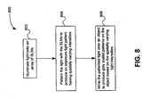
- FIG. 8 shows a flow chart depicting a method 800 according to the present invention.
- step 802 light is illuminated onto an array of SLMs.
- step 804 the light is patterned with the SLMs to produce an exposure light pattern having spatially varying intensities.
- step 806 the patterned light is written onto an object to produce gray scaled patterns on the object based on the spatially varying light intensities.
- the above methods and system allow for increase gray scale levels without increasing a conventional number of passes and/or pulses than conventionally done. Also, for analog SLMs, the above methods and systems allow for enhancing a number of gray scale levels beyond what is already mechanically feasible without increasing a conventional number of passes or pulses.
Landscapes
- Physics & Mathematics (AREA)
- General Physics & Mathematics (AREA)
- Exposure Of Semiconductors, Excluding Electron Or Ion Beam Exposure (AREA)
- Exposure And Positioning Against Photoresist Photosensitive Materials (AREA)
Applications Claiming Priority (2)
| Application Number | Priority Date | Filing Date | Title |
|---|---|---|---|
| US10/447,197 US20040239901A1 (en) | 2003-05-29 | 2003-05-29 | System and method for producing gray scaling using multiple spatial light modulators in a maskless lithography system |
| US447197 | 2003-05-29 |
Publications (1)
| Publication Number | Publication Date |
|---|---|
| EP1482367A2 true EP1482367A2 (de) | 2004-12-01 |
Family
ID=33131585
Family Applications (1)
| Application Number | Title | Priority Date | Filing Date |
|---|---|---|---|
| EP20040012133 Withdrawn EP1482367A2 (de) | 2003-05-29 | 2004-05-21 | System und Methode zur Herstellung von Graustufen durch die Verwendung von räumlichen Lichtmodulatoren in einem maskenlosen Lithographiesystem |
Country Status (7)
| Country | Link |
|---|---|
| US (1) | US20040239901A1 (de) |
| EP (1) | EP1482367A2 (de) |
| JP (1) | JP2004355006A (de) |
| KR (1) | KR20040103404A (de) |
| CN (1) | CN1573562A (de) |
| SG (1) | SG110095A1 (de) |
| TW (1) | TW200508691A (de) |
Families Citing this family (18)
| Publication number | Priority date | Publication date | Assignee | Title |
|---|---|---|---|---|
| US7023526B2 (en) * | 2003-09-30 | 2006-04-04 | Asml Holding N.V. | Methods and systems to compensate for a stitching disturbance of a printed pattern in a maskless lithography system utilizing overlap without an explicit attenuation |
| US6876440B1 (en) * | 2003-09-30 | 2005-04-05 | Asml Holding N.V. | Methods and systems to compensate for a stitching disturbance of a printed pattern in a maskless lithography system utilizing overlap of exposure zones with attenuation of the aerial image in the overlap region |
| US7410736B2 (en) * | 2003-09-30 | 2008-08-12 | Asml Holding N.V. | Methods and systems to compensate for a stitching disturbance of a printed pattern in a maskless lithography system not utilizing overlap of the exposure zones |
| US7336290B2 (en) | 2004-01-07 | 2008-02-26 | Texas Instruments Incorporated | Method and apparatus for increasing a perceived resolution of a display |
| GB0415916D0 (en) * | 2004-07-16 | 2004-08-18 | Pilkington Plc | Glazing inspection |
| KR100875900B1 (ko) * | 2007-06-08 | 2008-12-26 | 재단법인서울대학교산학협력재단 | 마스크를 사용하지 아니하는 광유체적 리소그래피 시스템 |
| US8363209B2 (en) * | 2007-07-10 | 2013-01-29 | Lg Electronics Inc. | Method and apparatus to adjust misalignment of the maskless exposure apparatus |
| US9116346B2 (en) | 2007-11-06 | 2015-08-25 | Nikon Corporation | Illumination apparatus, illumination method, exposure apparatus, and device manufacturing method |
| US9846689B2 (en) | 2008-01-29 | 2017-12-19 | Adobe Systems Incorporated | Method and system to provide portable database functionality in an electronic form |
| KR101008024B1 (ko) * | 2008-10-20 | 2011-01-14 | 삼성전자주식회사 | 바이오칩 제조 장치 |
| CN102621816B (zh) * | 2012-02-29 | 2013-11-27 | 天津芯硕精密机械有限公司 | 直写式光刻系统中采用灰度方式提高曝光图形质量的方法 |
| CN102902164B (zh) * | 2012-09-19 | 2015-04-22 | 天津芯硕精密机械有限公司 | 直写式光刻机在步进式曝光时的二维拼接处理方法 |
| DE102014203041A1 (de) | 2014-02-19 | 2015-08-20 | Carl Zeiss Smt Gmbh | Beleuchtungssystem einer mikrolithographischen Projektionsbelichtungsanlage und Verfahren zum Betreiben eines solchen |
| US9477161B2 (en) * | 2014-02-21 | 2016-10-25 | Palo Alto Research Center Incorporated | Method and system to operate arrays of reflective elements for extended lifetime operation in use with high intensity power light sources |
| CN106019857B (zh) * | 2016-07-22 | 2018-02-02 | 合肥芯碁微电子装备有限公司 | 一种基于无掩膜直写系统套刻曝光的定位方法 |
| JP7023601B2 (ja) | 2016-11-14 | 2022-02-22 | 株式会社アドテックエンジニアリング | ダイレクトイメージング露光装置及びダイレクトイメージング露光方法 |
| EP3605231A1 (de) * | 2018-08-01 | 2020-02-05 | ASML Netherlands B.V. | Optische maskenlose lithographie |
| CN114488713A (zh) * | 2022-02-18 | 2022-05-13 | 西湖大学 | 一种光刻机以及物理光刻方法 |
Family Cites Families (8)
| Publication number | Priority date | Publication date | Assignee | Title |
|---|---|---|---|---|
| US5748164A (en) * | 1994-12-22 | 1998-05-05 | Displaytech, Inc. | Active matrix liquid crystal image generator |
| US5691541A (en) * | 1996-05-14 | 1997-11-25 | The Regents Of The University Of California | Maskless, reticle-free, lithography |
| US6312134B1 (en) * | 1996-07-25 | 2001-11-06 | Anvik Corporation | Seamless, maskless lithography system using spatial light modulator |
| SE9800665D0 (sv) * | 1998-03-02 | 1998-03-02 | Micronic Laser Systems Ab | Improved method for projection printing using a micromirror SLM |
| US6498685B1 (en) * | 1999-01-11 | 2002-12-24 | Kenneth C. Johnson | Maskless, microlens EUV lithography system |
| US6425669B1 (en) * | 2000-05-24 | 2002-07-30 | Ball Semiconductor, Inc. | Maskless exposure system |
| US6544698B1 (en) * | 2001-06-27 | 2003-04-08 | University Of South Florida | Maskless 2-D and 3-D pattern generation photolithography |
| US7302111B2 (en) * | 2001-09-12 | 2007-11-27 | Micronic Laser Systems A.B. | Graphics engine for high precision lithography |
-
2003
- 2003-05-29 US US10/447,197 patent/US20040239901A1/en not_active Abandoned
-
2004
- 2004-05-21 EP EP20040012133 patent/EP1482367A2/de not_active Withdrawn
- 2004-05-26 TW TW093115004A patent/TW200508691A/zh unknown
- 2004-05-28 CN CNA2004100476688A patent/CN1573562A/zh active Pending
- 2004-05-28 KR KR1020040038111A patent/KR20040103404A/ko not_active Ceased
- 2004-05-28 SG SG200402997A patent/SG110095A1/en unknown
- 2004-05-31 JP JP2004162316A patent/JP2004355006A/ja active Pending
Also Published As
| Publication number | Publication date |
|---|---|
| KR20040103404A (ko) | 2004-12-08 |
| SG110095A1 (en) | 2005-04-28 |
| TW200508691A (en) | 2005-03-01 |
| CN1573562A (zh) | 2005-02-02 |
| JP2004355006A (ja) | 2004-12-16 |
| US20040239901A1 (en) | 2004-12-02 |
Similar Documents
| Publication | Publication Date | Title |
|---|---|---|
| US7463402B2 (en) | Using time and/or power modulation to achieve dose gray-scale in optical maskless lithography | |
| US7403266B2 (en) | Maskless lithography systems and methods utilizing spatial light modulator arrays | |
| EP1482367A2 (de) | System und Methode zur Herstellung von Graustufen durch die Verwendung von räumlichen Lichtmodulatoren in einem maskenlosen Lithographiesystem | |
| EP1491958B1 (de) | Optisches Projektionssystem für maskenlose Lithographie | |
| US7227613B2 (en) | Lithographic apparatus having double telecentric illumination | |
| US6989920B2 (en) | System and method for dose control in a lithographic system | |
| US7006295B2 (en) | Illumination system and method for efficiently illuminating a pattern generator | |
| US7414701B2 (en) | Method and systems for total focus deviation adjustments on maskless lithography systems | |
| US7242456B2 (en) | System and method utilizing a lithography tool having modular illumination, pattern generator, and projection optics portions |
Legal Events
| Date | Code | Title | Description |
|---|---|---|---|
| PUAI | Public reference made under article 153(3) epc to a published international application that has entered the european phase |
Free format text: ORIGINAL CODE: 0009012 |
|
| AK | Designated contracting states |
Kind code of ref document: A2 Designated state(s): AT BE BG CH CY CZ DE DK EE ES FI FR GB GR HU IE IT LI LU MC NL PL PT RO SE SI SK TR |
|
| AX | Request for extension of the european patent |
Extension state: AL HR LT LV MK |
|
| STAA | Information on the status of an ep patent application or granted ep patent |
Free format text: STATUS: THE APPLICATION IS DEEMED TO BE WITHDRAWN |
|
| 18D | Application deemed to be withdrawn |
Effective date: 20060201 |