EP1482412B1 - Arbitrage de mémoire partagée - Google Patents
Arbitrage de mémoire partagée Download PDFInfo
- Publication number
- EP1482412B1 EP1482412B1 EP03101577A EP03101577A EP1482412B1 EP 1482412 B1 EP1482412 B1 EP 1482412B1 EP 03101577 A EP03101577 A EP 03101577A EP 03101577 A EP03101577 A EP 03101577A EP 1482412 B1 EP1482412 B1 EP 1482412B1
- Authority
- EP
- European Patent Office
- Prior art keywords
- data
- read
- write
- unit
- storage unit
- Prior art date
- Legal status (The legal status is an assumption and is not a legal conclusion. Google has not performed a legal analysis and makes no representation as to the accuracy of the status listed.)
- Expired - Lifetime
Links
Images


Classifications
-
- G—PHYSICS
- G06—COMPUTING OR CALCULATING; COUNTING
- G06F—ELECTRIC DIGITAL DATA PROCESSING
- G06F13/00—Interconnection of, or transfer of information or other signals between, memories, input/output devices or central processing units
- G06F13/14—Handling requests for interconnection or transfer
- G06F13/16—Handling requests for interconnection or transfer for access to memory bus
- G06F13/1605—Handling requests for interconnection or transfer for access to memory bus based on arbitration
Definitions
- the present invention relates to an arbitration unit, to a channel, and to a method for arbitrating accesses to a shared storage.
- An electric or electronic system may comprise functional units that output data that has to be written to some kind of storage. There might exist different latency requirements with regard to the output data of the various functional units. Besides that, said functional units might generate different bandwidths of output data. Alternatively or additionally, said system might comprise functional units that have to be provided with input data that has to be read from some kind of storage. For some of these functional units, a low latency read access might be required. For other functional units, a high latency might be acceptable. Some functional units might require a high bandwidth of read data, while for others, a low bandwidth might be sufficient.
- US2002/0046261 discloses a memory controller having a time-division multiplexed interface to sources and destinations of data and a streaming interface to a memory. Each source and destination is identified by a context code. An arbiter specifies the context having the greatest requirement for memory access.
- the object is solved by the independent claims. Preferred embodiments are shown by the dependent claims.
- the arbitration unit is adapted for controlling accesses to a shared storage.
- the arbitration unit comprises a set of interfaces that connect a plurality of units with said arbitration unit. Outgoing data streams are transmitted from the arbitration unit via respective ones of said interfaces to at least one of said units, and incoming data streams are transmitted from at least one of said units via respective ones of said interfaces to the arbitration unit.
- the arbitration unit further comprises a control logic that is connected to each of said interfaces. Said control logic is adapted for segmenting write data of incoming data streams in order to set up write accesses to said shared storage, for scheduling a sequence of at least one of write and read accesses to said shared storage, and for distributing read data obtained during said read accesses to outgoing data streams.
- the arbitration unit might e.g. receive a stream of write data from one of said units.
- a block of write data that has been received via one of said interfaces is broken up into a plurality of smaller data packets, whereby the size of the data packets is such that they can be written to the shared storage during one single write access.
- the arbitration unit might have to handle read requests that are issued by one or more of said units.
- the arbitration unit might perform read accesses to the shared storage.
- the arbitration unit schedules a sequence of at least one of write and read accesses to the shared storage, whereby "scheduling" shall mean to define the temporal order of said write and read accesses.
- the data that is obtained from the storage during the read accesses might be reassembled into data blocks. Said data blocks might be transmitted, via one of the interfaces, to a respective unit, in order to fulfil the read request of said unit.
- the arbitration unit can be adapted in many ways to the properties of said units.
- the requirements imposed by said units can e.g. be considered by scheduling the memory accesses accordingly.
- the arbitration unit may choose the temporal order of the memory accesses in dependence on the required properties of the incoming or outgoing data streams, e.g. in dependence on the bandwidth or the latency required for a certain data stream. For example, a low latency read access might have to be scheduled immediately. For performing a high throughput write access, it might be necessary to perform a series of consecutive write accesses.
- each one of said read or write accesses must not take too long.
- the size of the data packets transferred during a single memory access is chosen in accordance with a trade off between latency and throughput.
- one or more of the interfaces comprise buffers that are adapted for buffering at least one of the incoming and outgoing data streams.
- said buffers are realized as FIFO (First In First Out) buffers.
- FIFO First In First Out
- write data that is received via said interface can be buffered. Even if the corresponding write access cannot be scheduled immediately, the write data can be accepted immediately.
- the read data that has been fetched from the memory might as well be buffered in a buffer, in order to provide a continuous data stream to the respective unit that has requested said data.
- each of the interfaces is connected with a respective one of the functional units.
- each of the interfaces is assigned to a certain one of the functional units, and the respective properties of said functional unit can be taken into account.
- Incoming data streams that are received from a certain functional unit via said interface can be processed in accordance with the requirements imposed by said functional unit.
- Also outgoing data streams that are routed via said interface to a certain functional unit can be processed in accordance with the properties of said functional unit.
- one or more of the units transmit read requests to the arbitration unit, whereby at least some of said read requests indicate a start address and a size of a data block that is to be read from the shared storage.
- One or more of the functional units might as well transfer write requests to the arbitration unit before a corresponding stream of write data is sent from the respective functional unit to the arbitration unit, whereby at least one of said write requests might indicate the size of the block of write data and a start address.
- the arbitration unit converts each of the read or write requests into a number of corresponding read or write accesses. As soon as the arbitration unit has received a respective read request or write request, it can start scheduling the corresponding read accesses or write accesses. Said requests, which are received some time in advance, are helpful for generating an optimized sequence of read and write accesses.
- said read and write accesses to the shared memory are scheduled in accordance with priorities that are assigned to at least some of the arbitration unit's interfaces, or to at least some of the incoming and outgoing data streams.
- the temporal order of the read and write accesses is determined by the control logic of the arbitration unit. If a high priority is assigned to an incoming data stream, the write accesses corresponding to said incoming data stream will be processed more quickly than other read and write accesses. In case of a very high priority, the write accesses corresponding to said incoming data stream might even be scheduled immediately.
- the corresponding read accesses will be carried out favorably, while low-priority write and read accesses will be postponed. As soon as the high-priority accesses have been processed, the low-priority accesses will be taken care of.
- a correspondingly high priority is assigned to said data stream.
- assigning a high priority it can be achieved that the corresponding read or write accesses are scheduled more quickly than other read and write accesses.
- a low-latency storage access can be provided.
- the arbitration unit's control logic allows to fulfill different kinds of latency requirements imposed by the functional units.
- the priorities are modified in a way that the amount of switching between read accesses and write accesses is kept small. Each time said switching is performed, an extra delay will occur. In order to avoid said extra delays, it is preferable to first process a group of write accesses, followed by a group of read accesses, etc. When a read access is being processed, it will be most favorable if the following memory access is a read access as well. This can e.g. be achieved by incrementing the priorities of the read requests, while the priorities of the write requests are kept constant. In contrary, when a write access is being performed, it is most favorable to process a write request next. In this case, one might e.g. increase the priorities assigned to the write requests, while the priorities of the read requests are kept constant.
- the priorities assigned to the read requests and to the write requests are modified in a way that a continuous transmission of data is promoted. If several memory accesses that relate to adjacent address ranges have to be processed, said memory accesses should preferably be carried out in succession in order to avoid any time delays due to re-addressing. Therefore, when a memory access that relates to a certain address range is processed, the priorities assigned to memory accesses that relate to adjacent address ranges are increased, and as a consequence, said memory accesses will most probably be scheduled next. As a consequence, an uninterrupted transmission of data is enhanced, and the amount of extra time delays due to re-addressing is kept small.
- the priority that is assigned to a certain interface is modified in dependence on the fill level of the buffer that corresponds to said interface.
- the arbitration unit is employed in a channel of an automated test equipment (ATE).
- the channel is responsible for at least one of: providing stimulus data to at least one device under test (DUT), and receiving response data from said at least one DUT.
- the channel's arbitration unit is responsible for coordinating the memory accesses to a shared storage.
- Said shared storage might e.g. be adapted for storing at least one of instructions and sequencer data. Said instructions and said sequencer data might be used for generating a stream of test data.
- the shared memory might as well be utilized for storing result data that is obtained by evaluating response data obtained from the at least one DUT.
- a channel of an automated test equipment encompassed at least two different memories, a low-latency SRAM adapted for providing a stream of instructions to a sequencer unit, and a high-latency DRAM adapted for storing sequencer data as well as result data.
- said at least two distinct memories are replaced by one shared memory that is controlled by an arbitration unit.
- the shared memory might e.g. be used for storing at least one of instructions, vector data, and result data.
- the set-up of the channel is simplified.
- a channel according to an embodiment of the present invention is cheaper and smaller than a channel according to the prior art.
- the units of said channel comprise at least one of: a sequencer, a result processing unit, an interface module, and a microprocessor core.
- the sequencer unit reads instructions and sequencer data from the shared memory and generates a stream of output data that might e.g. be provided to at least one of the drive path and the receive path of the channel.
- the result processing unit is responsible for evaluating the response data obtained from said at least one DUT.
- the result processing unit might generate a stream of result data that is written to the shared memory.
- the interface module is adapted for establishing a data link between the channel and a central facility. Via said interface module, data might be exchanged between the channel's shared memory and said central facility.
- the channel might comprise a microprocessor core.
- outgoing data streams are transmitted from the arbitration unit to the sequencer, whereby said outgoing data streams might comprise at least one of instructions and sequencer data.
- said outgoing data streams might comprise at least one of instructions and sequencer data.
- a high priority is assigned to an outgoing data stream that comprises instructions for said sequencer.
- the arbitration unit is adapted for receiving an incoming data stream from the result processing unit, whereby said incoming data stream might comprise result data.
- Said result data might e.g. be generated by comparing response data obtained from said at least one DUT with expected data.
- the arbitration unit exchanges data streams of high priority with said interface module. Especially if there do not exist any handshake signals, data that is exchanged between the interface module and the arbitration unit will have to be taken care of immediately.
- the shared storage is implemented as a dynamic RAM.
- a dynamic RAM (DRAM) is cheaper and smaller than a SRAM.
- a RDRAM comprising a synchronous clocked interface is employed. Due to said clocked interface, a data exchange of high bandwidth can be realized.
- the arbitration unit comprises a memory maintenance unit, whereby said memory maintenance unit forwards maintenance requests to the shared storage.
- said maintenance requests might for example comprise requests for performing a memory refresh.
- the invention can be partly or entirely embodied or supported by one or more suitable software programs, which can be stored on or otherwise provided by any kind of data carrier, and which might be executed in or by any suitable data processing unit.
- Software programs or routines are preferably applied for scheduling the sequence of write and read accesses to the shared storage.
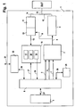
- a channel 1 of an automated test equipment is shown, whereby the channel 1 is responsible for at least one of: providing stimulus data to a DUT, and analyzing response data obtained from said DUT.
- the channel 1 doesn't have to be a channel of an automated test equipment; it might as well be a channel within any kind of multi-channel architecture.
- the channel 1 comprises a sequencer unit 2 that receives sequencer instructions 3 and sequencer data 4 from a shared memory 5 that is preferably implemented as a RDRAM. According to embodiments of the present invention, the shared memory 5 is accessed via an arbitration unit 6. If the DUT comprises at least one DRAM memory, the sequencer unit 2 might also read refresh data 7 from the shared memory 5. Said refresh data 7 is responsible for periodically initiating a refresh of the at least one DRAM memory within the DUT.
- the sequencer unit 2 generates an output data stream 8 that might comprise both drive data and expected data.
- the output data stream 8 is provided both to the drive path 9 and to the compare unit 10 of the receive path 11.
- the drive path 9 comprises a waveform table, which is a look-up table adapted for converting the vectors of the output data stream 8 into a corresponding sequence of waveforms.
- Each waveform comprises a set of edges, together with timing information for said edges.
- a stream of stimulus data 12 is obtained, and said stream of stimulus data 12 is provided to the pin 13 of the DUT.
- a stream of response data 14 might be obtained from the pin 13 of the DUT.
- the response data 14 is compared with expected data that is transmitted as a part of the output data stream 8. For this reason, the output data stream 8 is also provided to the compare unit 10 of the receive path 11.
- the compare unit 10 generates a stream of result data 15 comprising the results of the comparison. Said stream of result data 15 is provided to the result processing unit 16.
- the result processing unit 16 comprises a counter 17 that keeps track of the error count.
- the result processing unit 16 generates an error map 18 by recording the results as a function of the respective cycle.
- the error map data 19 is written, via the arbitration unit 6, to the shared memory 5.
- the result processing unit 16 generates an overview map 20, with one bit of said overview map representing 4 kByte of result data 15.
- cycle mask data 21 that is read from the shared memory 5 is provided to the result processing unit 16. Said cycle mask data 21 defines those parts of the result data stream 15 that have to be masked out.
- the shared memory 5 contains sequencer instructions, sequencer data and cycle mask data. Besides that, the shared memory 5 contains result data that is received from the result processing unit 16.
- the channel 1 For exchanging the shared memory's content with a workstation, the channel 1 comprises a workstation interface 22 adapted for establishing a data link 23 with the workstation. Via the workstation interface 22, data 24 can be exchanged between the workstation and the shared memory 5. Said data 24 is routed via the arbitration unit 6.
- the channel 1 comprises an embedded microprocessor core 25. Between said microprocessor core 25 and the shared memory 5, data 26 might be exchanged as well, whereby said data is also routed via the arbitration unit 6.
- the arbitration unit 6 segments write data of incoming data streams into corresponding data packets in order to set up write accesses to the shared memory 5.
- Said incoming data streams might comprise streams of result data 19, of data 24 exchanged with the workstation interface 22, and of data 26 exchanged with the embedded microprocessor core 25.
- the arbitration unit 6 schedules a sequence of write and read accesses to the shared memory 5. Read data obtained during the read accesses is distributed to the outgoing data streams.
- Said outgoing data streams might comprise the sequencer instructions 3, the sequencer data 4, the refresh data 7, and the cycle mask data 21.
- the outgoing data streams might also comprise data 24 for the workstation interface 22, and data 26 for the embedded microprocessor core 25.
- the channel's memory unit comprises a RDRAM memory 28, a RAM controller 29, and an arbitration unit 30.
- the arbitration unit 30 comprises a set of interfaces 31-37 for the various incoming and outgoing data streams. Via a first interface 31, data is exchanged with the workstation interface 22 shown in Fig. 1.
- the workstation may write to and read from the shared memory, and therefore, the corresponding request req may be a write request or a read request.
- a write request is adapted for indicating the start address of the write access and the size of the data block that is to be written to the shared memory.
- the start address and the size of a data block that is to be read from the shared memory are specified.
- write data Dw is buffered in a FIFO (First In First Out) buffer 38.
- the FIFO buffer 38 issues so-called slice requests sreq to the arbitration unit 30. There, priorities are assigned to the slice requests of the various interfaces, and the slice requests are handled in accordance with their respective priorities.
- priorities ranging from “1" to “9” are assigned to the various slice requests.
- the priority assigned to a data stream that is transmitted via one of the interfaces is modified in dependence on the corresponding FIFO buffer's fill level. For example, in case the FIFO buffer 38 is empty, a priority of "7" is assigned to a slice request sreq that corresponds to the first interface 31.
- the priority assigned to the slice request sreq of the first interface 31 is increased from "7" to "8” or "9” in dependence on the fill level of the FIFO buffer 38.
- the workstation interface 22 might as well transmit a read request to the FIFO buffer 38.
- One or more slice requests sreq corresponding to said read request are forwarded to the arbitration unit 30 and there, priorities ranging from "7" to "9" are assigned to said slice requests.
- the arbitration unit 30 receives slice requests sreq from all the interfaces that are connected to said arbitration unit 30.
- the arbitration unit 30 schedules a sequence of write and read data slices, whereby each of said data slices is of fixed size. For example, each of said data slices might comprise 256 bits of data.
- the write data Dw of a data block received via the interface 31 is broken up into a number of data slices, with each data slice comprising 256 bit of write data. Said data slices are scheduled in accordance with their respective priority. Then, said data slices are transmitted, as a part of a slice train 39, from the arbitration unit 30 to the RAM controller 29.
- the slice train 39 also comprises data slices that have been read from the shared memory, and each of said data slices also comprises 256 bit of read data.
- the RAM controller 29 exchanges read and write data 40 with the RDRAM memory 28.
- the workstation interface 22 has issued a read request to the first interface 31.
- Slice requests that correspond to said read request are transmitted to the arbitration unit 30.
- the data slices are scheduled by the arbitration unit 30, and the corresponding read accesses are performed by the RAM controller 29.
- the obtained data slices of read data are transmitted from the RAM controller 29 to the arbitration unit 30.
- data slices corresponding to various outgoing data streams are received and distributed to the FIFO buffers of the corresponding interfaces.
- the data slices that relate to the read request issued by the workstation interface 22 are written in sequential order to the FIFO buffer 38.
- the FIFO buffer 38 comprises a buffer for buffering incoming data as well as a buffer for buffering outgoing data.
- the workstation interface 22 can fetch the requested data block of read data Dr from the FIFO buffer 38.
- sequencer instructions are provided to the sequencer unit 2 shown in Fig. 1.
- the requested sequencer instructions are read from the RDRAM memory 28 and are transmitted within the slice train 39 to the arbitration unit 30.
- the arbitration unit 30 writes said sequencer instructions to the FIFO buffer 41.
- the third interface 33 is responsible for providing sequencer data to the sequencer unit 2. Sequencer data that has been read from the shared memory is buffered in a corresponding FIFO buffer 42.
- the fourth interface 34 is adapted for providing refresh data to the sequencer unit 2. Refresh data that has been read from the shared memory is buffered in the FIFO buffer 43.
- the error map 18, which is part of the result processing unit 16 shown in Fig. 1, provides a stream of result data to the fifth interface 35 of the arbitration unit 30.
- the result data is buffered in a FIFO buffer 44.
- the stream of cycle mask data is an outgoing data stream that is provided to the result processing unit 16 of Fig. 1.
- the cycle mask data that has been read from the RDRAM memory 28 is buffered in the FIFO buffer 45. Via the sixth interface 36, the cycle mask data is forwarded to the result processing unit 16.
- the seventh interface 37 is adapted for exchanging data with the embedded microprocessor core 25 of Fig. 1.
- the corresponding FIFO buffer 46 comprises a buffer for buffering incoming data as well as a buffer for buffering outgoing data.
- Fig. 2 the respective priorities that are assigned to the incoming and outgoing data streams of the various interfaces are depicted.
- the three priorities that are shown for each one of the interfaces 31-37 correspond to different fill levels of the respective FIFO buffers 38, 41-46.
- the highest priority is assigned to data that is exchanged, via the interface 31, with the workstation. Data that is provided by the workstation has to be processed immediately, because there do not exist any handshaking signals between the arbitration unit, the workstation interface and the workstation.
- Maintenance requests 47 that relate to the maintenance of the RDRAM memory 28 are generated by the RAM controller 29.
- Said maintenance requests 47 might for example comprise requests for performing a refresh of the RDRAM memory 28.
- the maintenance requests 47 are forwarded to the maintenance unit 48.
- slice requests are transmitted from the maintenance unit 48 to the arbitration unit 30. Initially, the priority "1" is assigned to a maintenance request. After some time, it is checked whether the maintenance request has been processed or not. If the maintenance request has not been processed yet, the priority of said maintenance request is increased to "5". After some more time has elapsed, it is checked once more whether the maintenance request has been taken care of. If the maintenance request still hasn't been processed, the priority is even set to "14" in order to enforce that the respective maintenance request is scheduled. Thus, it can be made sure that a periodic refresh of the RDRAM memory 28 is performed.
- Fig. 3 shows how a plurality of read and write requests are converted into a slice train 49, whereby the time that has elapsed is indicated from the left to the right.
- a first read request 51 is received via an interface A, whereby said read request specifies both the start address ("0") and the size ("96 byte") of the data block that has to be read from the memory.
- the first read request 51 might for example be a read request for reading sequencer data from the memory, and therefore, the priority "3" might be assigned to said first read request 51.
- An interface slice request 52 from interface A is set in order to indicate to the arbitration unit's control logic that a request with priority "3" from interface A has to be processed.
- the interface slice requests from interfaces A, B, and C are shown underneath the slice train 49.
- the next data slice of the slice train 49 has to be selected.
- the obtained data is transmitted, as a data slice 54, from the memory to the arbitration unit.
- the first reason why the priority of the interface slice request 55 is increased is that whenever a data slice comprising read data is transmitted, all the priorities of interface slice requests that correspond to read accesses are increased, while the priorities of interface slice requests that correspond to write accesses are kept constant. Whenever a data slice comprising write data is transmitted, the priorities of interface slice requests that correspond to write accesses are increased, while the priorities of interface slice requests that correspond to read accesses remain constant. By doing this, it can be achieved that the amount of switching between write accesses and read accesses is reduced. Any switching between write accesses and read accesses gives rise to an extra time delay that will further on be referred to as a "read-to-write bubble" or a "write-to-read bubble". By reducing the amount of switching between write accesses and read accesses, said extra time delays are reduced, and the RDRAM memory can be accessed more efficiently.
- the second reason why the priority of the interface slice request 55 is increased is that after a certain data slice has been transmitted, the priority of data slices that relate to an adjacent address range is increased in order to promote continuous read and write operations.
- the priorities of subsequent data slices might e.g. be incremented by one. By doing this, extra time delays due to re-addressing, which will further on be referred to as "re-addressing bubbles", are reduced.
- the priority of the interface slice request 55 is incremented from “3" to "4" in order to avoid any switching between read and write operations, and said priority is further increased from "4" to "5" in order to promote the transmission of an adjacent block of data.
- a write request 59 is received by the arbitration unit 30 via an interface B.
- the write request 59 indicates that 64 byte of write data starting at the address 256 have to be written to the memory.
- Said write data might e.g. be a block of result data, and correspondingly, a priority of "5" might be assigned to said write data.
- the interface slice request 60 from interface B is set.
- a second read request 61 is received at the point of time 62, and said second read request 61 indicates that 32 byte of read data have to be read from the memory starting at the address 512.
- the read request 61 which is received via the interface C, might for example relate to fetching instructions from the memory, and therefore, a priority of "6" might initially be assigned to said read request.
- a read access is being processed. In order to avoid any switching from read to write, the priority of the second read request 61 is incremented from "6" to "7".
- the interface slice request 63 from interface C is set.
- the transmission of the data slice 57 is finished at the point of time 64.
- the interface slice request 65 from interface A is still active, because the first read request 51 hasn't been completed yet.
- a third data slice corresponding to the first read request 51 still has to be transmitted.
- the priority "7" of the interface slice request 63 is higher than the respective priorities of the interface slice requests 60 and 65. Accordingly, a data slice 67 that corresponds to the second read request 61 is scheduled next.
- the data slice 67 is transmitted, said data slice 67 comprising 32 bytes of read data from the addresses 512 to 544.
- a third data slice 81 corresponding to the first read request 51 is transmitted from the shared memory to the arbitration unit.
- Said data slice 81 comprises 32 byte of read data that have been read from the memory addresses 64 to 96.
Landscapes
- Engineering & Computer Science (AREA)
- Theoretical Computer Science (AREA)
- Physics & Mathematics (AREA)
- General Engineering & Computer Science (AREA)
- General Physics & Mathematics (AREA)
- Multi Processors (AREA)
- Information Transfer Systems (AREA)
- Memory System (AREA)
Claims (22)
- Unité de mémoire dans un canal d'un dispositif de test, comprenant :une mémoire partagée (5, 28) ;une unité d'arbitrage (6, 30) adaptée pour contrôler les accès à une mémoire partagée (5, 28), ladite unité d'arbitrage comprenant :un ensemble d'interfaces (31-37) adaptées pour connecter une pluralité d'unités à ladite unité d'arbitrage (6, 30), dans lequel des trains de données sortants sont transmis à partir de l'unité d'arbitrage (6, 30), par l'intermédiaire de celles respectives desdites interfaces, vers au moins l'une desdites unités, et dans lequel les trains de données entrants sont transmis à partir de l'une au moins desdites unités, par l'intermédiaire de celles respectives desdites interfaces, vers l'unité d'arbitrage (6, 30) ;une logique de commande qui est connectée à chacune desdites interfaces (31 - 37), ladite unité de commande étant adaptée pour segmenter des données d'écriture des trains de données entrants afin d'établir des accès d'écriture vers ladite mémoire partagée, pour planifier une séquence (49) de l'un au moins des accès d'écriture et de lecture à ladite mémoire partagée (5, 28), et pour répartir les données lues obtenues au cours desdits accès de lecture vers les trains de données sortants, etau moins un tampon, de préférence au moins un tampon FIFO (38, 41 - 46), qui est adapté pour tamponner un ou plusieurs des trains de données entrants et sortants.
- Unité de mémoire selon la revendication 1, dans laquelle au moins une desdites interfaces comprend au moins un tampon, de préférence au moins un tampon FIFO (38, 41 - 46), qui est adapté pour tamponner un ou plusieurs des trains de données entrants et sortants.
- Unité de mémoire selon la revendication 1 ou l'une quelconque des revendications précédentes, dans laquelle chacune desdites interfaces est connectée à l'une respective desdites unités.
- Unité de mémoire selon la revendication 1 ou l'une quelconque des revendications précédentes, dans laquelle au moins une desdites unités est adaptée pour transmettre à l'unité d'arbitrage, au moins l'une des demandes d'écriture (59) ou des demandes de lecture (51, 61), dans laquelle au moins l'une des demandes d'écriture indique une adresse de début et une taille du bloc de données qui doit être écrit dans ladite mémoire partagée, et dans laquelle au moins une demande de lecture indique une adresse de début et une taille du bloc de données qui doit être lu de ladite mémoire partagée.
- Unité de mémoire selon la revendication 1 ou l'une quelconque des revendications précédentes, dans laquelle ladite logique de commande est adaptée pour planifier lesdits accès de lecture et lesdits accès d'écriture sur la base des priorités qui sont affectées à certaines au moins des diverses interfaces, ou à certains au moins des divers trains de données entrants et sortants.
- Unité de mémoire selon la revendication 1 ou l'une quelconque des revendications précédentes, dans laquelle ladite logique de commande est adaptée pour prendre en considération un temps d'attente faible d'un train de données entrant ou sortant, en affectant une priorité proportionnellement élevée au train de données respectif.
- Unité de mémoire selon la revendication 5 ou l'une quelconque des revendications précédentes, dans laquelle ladite logique de commande est adaptée pour modifier lesdites priorités de telle manière que la quantité de commutation entre écriture et lecture, ou vice versa, soit maintenue petite.
- Unité de mémoire selon la revendication 5 ou l'une quelconque des revendications précédentes, dans laquelle ladite logique de commande est adaptée pour modifier lesdites priorités de telle manière qu'une transmission continue de l'un au moins desdits trains de données, soit favorisée.
- Unité de mémoire selon la revendication 5 ou l'une quelconque des revendications précédentes, dans laquelle ladite logique de commande est adaptée pour modifier lesdites priorités de telle manière que plus le niveau de remplissage d'un tampon devient élevé, plus la priorité du train de données tamponné correspondant devient élevée.
- Unité de mémoire selon la revendication 1 ou l'une quelconque des revendications précédentes, dans laquelle ladite unité d'arbitrage est adaptée pour être utilisée dans un canal d'un équipement de test automatisé pour coordonner les accès mémoire à ladite mémoire partagée, dans laquelle ledit canal est responsable de l'une au moins de : la délivrance de données de stimuli à un DUT au moins, et de la réception des données de réponse en provenance dudit un DUT au moins.
- Unité de mémoire selon la revendication 1 ou l'une quelconque des revendications précédentes, dans laquelle l'une au moins desdites unités représente au moins un parmi :un contrôleur de séquence (2), une unité de traitement de résultat (16), un module d'interface (22) adapté pour établir une liaison de transmission de données (23) entre le canal et une installation centrale, et un coeur de microprocesseur (25).
- Unité de mémoire selon la revendication 11, dans laquelle ladite unité d'arbitrage est adaptée pour transmettre les trains de données sortants audit contrôleur de séquence (2), lesdits trains de données sortants comprenant au moins des instructions (3) et / ou des données du contrôleur de séquence (4).
- Unité de mémoire selon la revendication 12, dans laquelle ladite logique de commande est adaptée pour affecter une priorité élevée à un train de données sortant qui comprend des instructions dudit contrôleur de séquence.
- Unité de mémoire selon la revendication 11 ou l'une quelconque des revendications précédentes, dans laquelle ladite unité d'arbitrage est adaptée pour recevoir un train de données entrant à partir de ladite unité de traitement de résultat (16), ledit train de données entrant comprenant des données de résultat (19) qui doivent être écrites dans ladite mémoire partagée.
- Unité de mémoire selon la revendication 11 ou l'une quelconque des revendications précédentes, dans laquelle ladite unité d'arbitrage est adaptée pour échanger des trains de données (24) avec ledit module d'interface (22), dans laquelle un priorité élevée est affectée auxdits trains de données (24).
- Unité de mémoire selon la revendication 1 ou l'une quelconque des revendications précédentes, dans laquelle ladite mémoire partagée (5, 28) est une RAM dynamique, et de préférence une RDRAM.
- Unité de mémoire selon la revendication 1 ou l'une quelconque des revendications précédentes, comprenant de plus une unité de mise à jour de mémoire (48) adaptée pour fournir des demandes de mise à jour à ladite mémoire partagée.
- Canal (1) destiné à être utilisé dans un équipement de test automatisé, ledit canal comprenant :une unité de mémoire selon l'une quelconque des revendications précédentes ;un contrôleur de séquence (2) adapté pour lire des données à partir de ladite unité de mémoire, et pour délivrer des données de stimuli à un DUT au moins ; etune unité de traitement de résultat (16) adaptée pour évaluer les données de résultat (19) obtenues à partir dudit un DUT au moins, et pour écrire des données dans ladite unité de mémoire.
- Canal selon la revendication, 18, comprenant de plus un module d'interface (22) adapté pour établir une liaison de transmission de données (23) entre le canal (1) et une installation centrale.
- Équipement de test automatisé adapté pour tester un DUT au moins, ledit équipement de test automatisé comprenant :un canal (1) au moins selon l'une quelconque des revendications 18 ou 19 ; etune installation centrale adaptée pour coordonner ledit au moins un canal.
- Procédé pour arbitrer des accès à une mémoire partagée (5, 28) dans une unité de mémoire d'un canal d'un dispositif de test, ladite mémoire partagée (5, 28) pouvant être consultée par une pluralité d'unités, ledit procédé comprenant les étapes suivantes consistant à :segmenter les données d'écriture des trains de données entrants afin de fixer les accès d'écriture correspondants à ladite mémoire partagée (5, 28) ;planifier une séquence (49) d'accès d'écriture et de lecture à ladite mémoire partagée (5, 28) ;répartir les données de lecture obtenues au cours desdits accès de lecture vers les trains de données sortants.
- Programme ou produit logiciel, stocké de préférence sur un support de données, pour exécuter le procédé selon la revendication 21 une fois exécuté sur un système de traitement de données tel qu'un ordinateur ou un processeur de signaux numériques.
Priority Applications (4)
| Application Number | Priority Date | Filing Date | Title |
|---|---|---|---|
| EP03101577A EP1482412B1 (fr) | 2003-05-30 | 2003-05-30 | Arbitrage de mémoire partagée |
| DE60307798T DE60307798T2 (de) | 2003-05-30 | 2003-05-30 | Arbitrierung von gemeinsamen Speicher |
| US10/825,473 US7216182B2 (en) | 2003-05-30 | 2004-04-15 | Shared storage arbitration |
| JP2004158811A JP2004362567A (ja) | 2003-05-30 | 2004-05-28 | 共用記憶装置の調停 |
Applications Claiming Priority (1)
| Application Number | Priority Date | Filing Date | Title |
|---|---|---|---|
| EP03101577A EP1482412B1 (fr) | 2003-05-30 | 2003-05-30 | Arbitrage de mémoire partagée |
Publications (2)
| Publication Number | Publication Date |
|---|---|
| EP1482412A1 EP1482412A1 (fr) | 2004-12-01 |
| EP1482412B1 true EP1482412B1 (fr) | 2006-08-23 |
Family
ID=33104179
Family Applications (1)
| Application Number | Title | Priority Date | Filing Date |
|---|---|---|---|
| EP03101577A Expired - Lifetime EP1482412B1 (fr) | 2003-05-30 | 2003-05-30 | Arbitrage de mémoire partagée |
Country Status (4)
| Country | Link |
|---|---|
| US (1) | US7216182B2 (fr) |
| EP (1) | EP1482412B1 (fr) |
| JP (1) | JP2004362567A (fr) |
| DE (1) | DE60307798T2 (fr) |
Families Citing this family (19)
| Publication number | Priority date | Publication date | Assignee | Title |
|---|---|---|---|---|
| DE602004030487D1 (de) * | 2004-01-30 | 2011-01-20 | Ericsson Telefon Ab L M | Paketablaufsteuerung zur Datenstromübertragung |
| JP4012167B2 (ja) * | 2004-03-31 | 2007-11-21 | 株式会社東芝 | 無線通信システム |
| JP4181093B2 (ja) * | 2004-07-16 | 2008-11-12 | 株式会社東芝 | 無線通信システム |
| JP4275085B2 (ja) * | 2005-02-17 | 2009-06-10 | 株式会社ソニー・コンピュータエンタテインメント | 情報処理装置、情報処理方法、およびデータストリーム生成方法 |
| JP4847036B2 (ja) * | 2005-03-30 | 2011-12-28 | キヤノン株式会社 | バスアクセスを調停する制御装置およびデータ処理装置の制御方法 |
| US20080059672A1 (en) * | 2006-08-30 | 2008-03-06 | Irish John D | Methods and Apparatus for Scheduling Prioritized Commands on a Bus |
| US8307180B2 (en) | 2008-02-28 | 2012-11-06 | Nokia Corporation | Extended utilization area for a memory device |
| JP4752882B2 (ja) * | 2008-07-24 | 2011-08-17 | ソニー株式会社 | メモリアクセスシステム、メモリ制御装置、メモリ制御方法、および、プログラム |
| US8918566B2 (en) | 2009-01-23 | 2014-12-23 | Hewlett-Packard Development Company, L. P. | System and methods for allocating shared storage resources |
| US8713248B2 (en) * | 2009-06-02 | 2014-04-29 | Nokia Corporation | Memory device and method for dynamic random access memory having serial interface and integral instruction buffer |
| WO2013098463A1 (fr) | 2011-12-29 | 2013-07-04 | Nokia Corporation | Procédé d'effacement d'entité de données dans un module de mémoire |
| US10536565B2 (en) * | 2013-03-14 | 2020-01-14 | International Business Machines Corporation | Efficient centralized stream initiation and retry control |
| JP6146128B2 (ja) * | 2013-05-20 | 2017-06-14 | ヤマハ株式会社 | データ処理装置 |
| WO2015089488A1 (fr) | 2013-12-12 | 2015-06-18 | Memory Technologies Llc | Modules de mémorisation optimisée à canaux |
| JP5911548B1 (ja) | 2014-10-23 | 2016-04-27 | インターナショナル・ビジネス・マシーンズ・コーポレーションInternational Business Machines Corporation | 共有メモリへのアクセス要求をスケジューリングするための装置、方法およびコンピュータプログラム |
| US10048963B2 (en) * | 2016-05-23 | 2018-08-14 | International Business Machines Corporation | Executing system call vectored instructions in a multi-slice processor |
| FR3057970B1 (fr) * | 2016-10-26 | 2019-12-13 | Zodiac Aero Electric | Architecture de communication pour l'echange de donnees entre des unites de traitement |
| JP7695063B2 (ja) | 2020-09-30 | 2025-06-18 | 株式会社デンソー | 共用ストレージ管理装置及び共用ストレージ管理方法 |
| JP7625474B2 (ja) * | 2021-04-14 | 2025-02-03 | キヤノン株式会社 | メモリ制御回路、情報処理システム及びメモリ制御方法 |
Family Cites Families (14)
| Publication number | Priority date | Publication date | Assignee | Title |
|---|---|---|---|---|
| US5117486A (en) * | 1989-04-21 | 1992-05-26 | International Business Machines Corp. | Buffer for packetizing block of data with different sizes and rates received from first processor before transferring to second processor |
| CA2080608A1 (fr) * | 1992-01-02 | 1993-07-03 | Nader Amini | Logique de commande de bus pour ordinateur a deux bus |
| US5530838A (en) * | 1993-06-10 | 1996-06-25 | Ricoh Company, Ltd. | Method and apparatus for controlling access to memory which is common to plural, priority-ordered central processing units and which is indirectly accessible via a transfer control unit |
| US5630096A (en) * | 1995-05-10 | 1997-05-13 | Microunity Systems Engineering, Inc. | Controller for a synchronous DRAM that maximizes throughput by allowing memory requests and commands to be issued out of order |
| US5809538A (en) * | 1996-02-07 | 1998-09-15 | General Instrument Corporation | DRAM arbiter for video decoder |
| US5905876A (en) * | 1996-12-16 | 1999-05-18 | Intel Corporation | Queue ordering for memory and I/O transactions in a multiple concurrent transaction computer system |
| US5950229A (en) * | 1997-03-12 | 1999-09-07 | Micron Electronics, Inc. | System for accelerating memory bandwidth |
| US6088772A (en) * | 1997-06-13 | 2000-07-11 | Intel Corporation | Method and apparatus for improving system performance when reordering commands |
| US6092158A (en) * | 1997-06-13 | 2000-07-18 | Intel Corporation | Method and apparatus for arbitrating between command streams |
| US6442628B1 (en) * | 1998-05-01 | 2002-08-27 | Adaptec, Inc. | Method and system for automatically determining maximum data throughput over a bus |
| US6622272B1 (en) * | 2000-03-10 | 2003-09-16 | Teradyne, Inc. | Automatic test equipment methods and apparatus for interfacing with an external device |
| US20020046251A1 (en) * | 2001-03-09 | 2002-04-18 | Datacube, Inc. | Streaming memory controller |
| US6901500B1 (en) * | 2000-07-28 | 2005-05-31 | Silicon Graphics, Inc. | Method and apparatus for prefetching information and storing the information in a stream buffer |
| JP2004280926A (ja) * | 2003-03-14 | 2004-10-07 | Renesas Technology Corp | 半導体記憶装置 |
-
2003
- 2003-05-30 EP EP03101577A patent/EP1482412B1/fr not_active Expired - Lifetime
- 2003-05-30 DE DE60307798T patent/DE60307798T2/de not_active Expired - Lifetime
-
2004
- 2004-04-15 US US10/825,473 patent/US7216182B2/en not_active Expired - Fee Related
- 2004-05-28 JP JP2004158811A patent/JP2004362567A/ja active Pending
Also Published As
| Publication number | Publication date |
|---|---|
| US7216182B2 (en) | 2007-05-08 |
| EP1482412A1 (fr) | 2004-12-01 |
| DE60307798D1 (de) | 2006-10-05 |
| US20040243900A1 (en) | 2004-12-02 |
| DE60307798T2 (de) | 2006-12-14 |
| JP2004362567A (ja) | 2004-12-24 |
Similar Documents
| Publication | Publication Date | Title |
|---|---|---|
| EP1482412B1 (fr) | Arbitrage de mémoire partagée | |
| KR100716950B1 (ko) | 버스 시스템 | |
| CN103064807B (zh) | 多通道直接存储器存取控制器 | |
| US7644207B2 (en) | High speed bus for isolated data acquisition applications | |
| US20050193155A1 (en) | Data transfer apparatus and transfer control program | |
| US6868087B1 (en) | Request queue manager in transfer controller with hub and ports | |
| US20080276021A1 (en) | Data transfer control apparatus | |
| JPH04230557A (ja) | 直接メモリアクセス・コントローラ | |
| US10146468B2 (en) | Addressless merge command with data item identifier | |
| JP4184614B2 (ja) | バスシステム及びその実行順序の調整方法 | |
| US9804959B2 (en) | In-flight packet processing | |
| US7970959B2 (en) | DMA transfer system using virtual channels | |
| EP1752881A1 (fr) | Appareil destine a l'arbitrage de ressource de mémoire en fonction de l'attribution de l'intervalle de temps dédiée | |
| US9846662B2 (en) | Chained CPP command | |
| WO1996035172A1 (fr) | Controleur donnant acces a un tampon d'images dans un environnement de transactions sur bus dedouble | |
| US20020078267A1 (en) | Scheduler for a data memory access having multiple channels | |
| EP1653370A2 (fr) | Controleur de bus | |
| US6412049B1 (en) | Method for minimizing CPU memory latency while transferring streaming data | |
| CN119271622A (zh) | 片上信息的多路复用方法以及相关装置 | |
| US20040243770A1 (en) | Data transfer system | |
| WO2007099659A1 (fr) | Dispositif et procede de transmission de donnees | |
| KR20020096650A (ko) | 영상 처리기의 메모리 액세스 중재 장치 및 방법 | |
| JP4737702B2 (ja) | ディスクアレイ制御装置 | |
| US20060248240A1 (en) | Multi mode dma controller with transfer packet preprocessor | |
| JP4485503B2 (ja) | ディスクアレイ制御装置及びディスクアレイ制御方法 |
Legal Events
| Date | Code | Title | Description |
|---|---|---|---|
| PUAI | Public reference made under article 153(3) epc to a published international application that has entered the european phase |
Free format text: ORIGINAL CODE: 0009012 |
|
| AK | Designated contracting states |
Kind code of ref document: A1 Designated state(s): AT BE BG CH CY CZ DE DK EE ES FI FR GB GR HU IE IT LI LU MC NL PT RO SE SI SK TR |
|
| AX | Request for extension of the european patent |
Extension state: AL LT LV MK |
|
| 17P | Request for examination filed |
Effective date: 20050601 |
|
| 17Q | First examination report despatched |
Effective date: 20050628 |
|
| AKX | Designation fees paid |
Designated state(s): DE FR GB |
|
| GRAP | Despatch of communication of intention to grant a patent |
Free format text: ORIGINAL CODE: EPIDOSNIGR1 |
|
| GRAS | Grant fee paid |
Free format text: ORIGINAL CODE: EPIDOSNIGR3 |
|
| GRAA | (expected) grant |
Free format text: ORIGINAL CODE: 0009210 |
|
| AK | Designated contracting states |
Kind code of ref document: B1 Designated state(s): DE FR GB |
|
| REG | Reference to a national code |
Ref country code: GB Ref legal event code: FG4D |
|
| REF | Corresponds to: |
Ref document number: 60307798 Country of ref document: DE Date of ref document: 20061005 Kind code of ref document: P |
|
| RAP2 | Party data changed (patent owner data changed or rights of a patent transferred) |
Owner name: AGILENT TECHNOLOGIES, INC. |
|
| ET | Fr: translation filed | ||
| PLBE | No opposition filed within time limit |
Free format text: ORIGINAL CODE: 0009261 |
|
| STAA | Information on the status of an ep patent application or granted ep patent |
Free format text: STATUS: NO OPPOSITION FILED WITHIN TIME LIMIT |
|
| 26N | No opposition filed |
Effective date: 20070524 |
|
| GBPC | Gb: european patent ceased through non-payment of renewal fee |
Effective date: 20070530 |
|
| PGFP | Annual fee paid to national office [announced via postgrant information from national office to epo] |
Ref country code: FR Payment date: 20070828 Year of fee payment: 5 |
|
| PG25 | Lapsed in a contracting state [announced via postgrant information from national office to epo] |
Ref country code: GB Free format text: LAPSE BECAUSE OF NON-PAYMENT OF DUE FEES Effective date: 20070530 |
|
| REG | Reference to a national code |
Ref country code: FR Ref legal event code: ST Effective date: 20090119 |
|
| PG25 | Lapsed in a contracting state [announced via postgrant information from national office to epo] |
Ref country code: FR Free format text: LAPSE BECAUSE OF NON-PAYMENT OF DUE FEES Effective date: 20080602 |
|
| REG | Reference to a national code |
Ref country code: DE Ref legal event code: R082 Ref document number: 60307798 Country of ref document: DE Representative=s name: SCHOPPE, ZIMMERMANN, STOECKELER, ZINKLER & PAR, DE |
|
| REG | Reference to a national code |
Ref country code: DE Ref legal event code: R082 Ref document number: 60307798 Country of ref document: DE Representative=s name: SCHOPPE, ZIMMERMANN, STOECKELER, ZINKLER, SCHE, DE Effective date: 20120515 Ref country code: DE Ref legal event code: R081 Ref document number: 60307798 Country of ref document: DE Owner name: ADVANTEST (SINGAPORE) PTE. LTD., SG Free format text: FORMER OWNER: VERIGY (SINGAPORE) PTE. LTD., SINGAPORE, SG Effective date: 20120515 Ref country code: DE Ref legal event code: R082 Ref document number: 60307798 Country of ref document: DE Representative=s name: SCHOPPE, ZIMMERMANN, STOECKELER, ZINKLER & PAR, DE Effective date: 20120515 |
|
| PGFP | Annual fee paid to national office [announced via postgrant information from national office to epo] |
Ref country code: DE Payment date: 20130522 Year of fee payment: 11 |
|
| REG | Reference to a national code |
Ref country code: DE Ref legal event code: R119 Ref document number: 60307798 Country of ref document: DE |
|
| REG | Reference to a national code |
Ref country code: DE Ref legal event code: R119 Ref document number: 60307798 Country of ref document: DE Effective date: 20141202 |
|
| PG25 | Lapsed in a contracting state [announced via postgrant information from national office to epo] |
Ref country code: DE Free format text: LAPSE BECAUSE OF NON-PAYMENT OF DUE FEES Effective date: 20141202 |