EP1482566A2 - Elektrodenstruktur für Leuchtdiode und Vollfarbenleuchtdiode durch kaskadiertes überlappendes Die-Bonding - Google Patents
Elektrodenstruktur für Leuchtdiode und Vollfarbenleuchtdiode durch kaskadiertes überlappendes Die-Bonding Download PDFInfo
- Publication number
- EP1482566A2 EP1482566A2 EP03012081A EP03012081A EP1482566A2 EP 1482566 A2 EP1482566 A2 EP 1482566A2 EP 03012081 A EP03012081 A EP 03012081A EP 03012081 A EP03012081 A EP 03012081A EP 1482566 A2 EP1482566 A2 EP 1482566A2
- Authority
- EP
- European Patent Office
- Prior art keywords
- die
- led
- bonding pad
- led die
- positive
- Prior art date
- Legal status (The legal status is an assumption and is not a legal conclusion. Google has not performed a legal analysis and makes no representation as to the accuracy of the status listed.)
- Withdrawn
Links
Images






Classifications
-
- H—ELECTRICITY
- H10—SEMICONDUCTOR DEVICES; ELECTRIC SOLID-STATE DEVICES NOT OTHERWISE PROVIDED FOR
- H10H—INORGANIC LIGHT-EMITTING SEMICONDUCTOR DEVICES HAVING POTENTIAL BARRIERS
- H10H20/00—Individual inorganic light-emitting semiconductor devices having potential barriers, e.g. light-emitting diodes [LED]
- H10H20/80—Constructional details
- H10H20/83—Electrodes
- H10H20/831—Electrodes characterised by their shape
-
- H—ELECTRICITY
- H10—SEMICONDUCTOR DEVICES; ELECTRIC SOLID-STATE DEVICES NOT OTHERWISE PROVIDED FOR
- H10W—GENERIC PACKAGES, INTERCONNECTIONS, CONNECTORS OR OTHER CONSTRUCTIONAL DETAILS OF DEVICES COVERED BY CLASS H10
- H10W90/00—Package configurations
-
- H—ELECTRICITY
- H10—SEMICONDUCTOR DEVICES; ELECTRIC SOLID-STATE DEVICES NOT OTHERWISE PROVIDED FOR
- H10H—INORGANIC LIGHT-EMITTING SEMICONDUCTOR DEVICES HAVING POTENTIAL BARRIERS
- H10H20/00—Individual inorganic light-emitting semiconductor devices having potential barriers, e.g. light-emitting diodes [LED]
- H10H20/80—Constructional details
- H10H20/83—Electrodes
- H10H20/832—Electrodes characterised by their material
- H10H20/833—Transparent materials
-
- H—ELECTRICITY
- H10—SEMICONDUCTOR DEVICES; ELECTRIC SOLID-STATE DEVICES NOT OTHERWISE PROVIDED FOR
- H10H—INORGANIC LIGHT-EMITTING SEMICONDUCTOR DEVICES HAVING POTENTIAL BARRIERS
- H10H20/00—Individual inorganic light-emitting semiconductor devices having potential barriers, e.g. light-emitting diodes [LED]
- H10H20/80—Constructional details
- H10H20/84—Coatings, e.g. passivation layers or antireflective coatings
- H10H20/841—Reflective coatings, e.g. dielectric Bragg reflectors
-
- H—ELECTRICITY
- H10—SEMICONDUCTOR DEVICES; ELECTRIC SOLID-STATE DEVICES NOT OTHERWISE PROVIDED FOR
- H10W—GENERIC PACKAGES, INTERCONNECTIONS, CONNECTORS OR OTHER CONSTRUCTIONAL DETAILS OF DEVICES COVERED BY CLASS H10
- H10W72/00—Interconnections or connectors in packages
- H10W72/071—Connecting or disconnecting
- H10W72/075—Connecting or disconnecting of bond wires
- H10W72/07551—Connecting or disconnecting of bond wires characterised by changes in properties of the bond wires during the connecting
- H10W72/07554—Connecting or disconnecting of bond wires characterised by changes in properties of the bond wires during the connecting changes in dispositions
-
- H—ELECTRICITY
- H10—SEMICONDUCTOR DEVICES; ELECTRIC SOLID-STATE DEVICES NOT OTHERWISE PROVIDED FOR
- H10W—GENERIC PACKAGES, INTERCONNECTIONS, CONNECTORS OR OTHER CONSTRUCTIONAL DETAILS OF DEVICES COVERED BY CLASS H10
- H10W72/00—Interconnections or connectors in packages
- H10W72/50—Bond wires
- H10W72/541—Dispositions of bond wires
- H10W72/547—Dispositions of multiple bond wires
-
- H—ELECTRICITY
- H10—SEMICONDUCTOR DEVICES; ELECTRIC SOLID-STATE DEVICES NOT OTHERWISE PROVIDED FOR
- H10W—GENERIC PACKAGES, INTERCONNECTIONS, CONNECTORS OR OTHER CONSTRUCTIONAL DETAILS OF DEVICES COVERED BY CLASS H10
- H10W72/00—Interconnections or connectors in packages
- H10W72/50—Bond wires
- H10W72/551—Materials of bond wires
- H10W72/552—Materials of bond wires comprising metals or metalloids, e.g. silver
- H10W72/5522—Materials of bond wires comprising metals or metalloids, e.g. silver comprising gold [Au]
-
- H—ELECTRICITY
- H10—SEMICONDUCTOR DEVICES; ELECTRIC SOLID-STATE DEVICES NOT OTHERWISE PROVIDED FOR
- H10W—GENERIC PACKAGES, INTERCONNECTIONS, CONNECTORS OR OTHER CONSTRUCTIONAL DETAILS OF DEVICES COVERED BY CLASS H10
- H10W72/00—Interconnections or connectors in packages
- H10W72/50—Bond wires
- H10W72/551—Materials of bond wires
- H10W72/552—Materials of bond wires comprising metals or metalloids, e.g. silver
- H10W72/5524—Materials of bond wires comprising metals or metalloids, e.g. silver comprising aluminium [Al]
Definitions
- the present invention relates to a package structure of semiconductor light emitted diodes (LED), and more particularly, to a package and electrode structure of LEDs suitable for overlap bonding the LEDs in cascade by chip direct bonding with transparent layer and reflected metal layer, and capable of generating a full color light or white light by mixing lights emitted from the overlap LEDs
- LED semiconductor light emitted diodes
- LED Light emitted diode
- LED is a semiconductor light-emitting device, formed by a p-n junction, to transform electric power into a light source.
- LED has characteristics such as small volume, long life-time, low driving voltage, shock hardness, thermal stability, etc., suitable for applications which need to be thin and small, and used in traffic signals, back light source of LCD and other commercial products.
- LED make use of variety of compound semiconductor such as III-V group materials, II -VI group materials, to form variety structures such as p-n junction, double-hetero-junction(DH) and quantum well(QW), which can be used to design red, orange, yellow, green, blue, violet LEDs and also infrared, ultraviolet in-visible light LEDs.
- III-V group materials III-V group materials, II -VI group materials
- QW quantum well
- Materials suitable for making high intensity LED over 1000mcd with wave length from long wave to short wave are AlGaAs, InGaAIP and InGaN, etc.
- LEDs with different visible and invisible colors can be designed, wherein AIGaAs, InGaAIP and InGaN are suitable for producing LEDs with high luminance over 1000 mcd.
- an LPE Liquid Phase Epitaxy
- DE Double Epitaxy
- InGaAIP can be used to produce red, orange, yellow and yellow-green LEDs, and an MOVPE (Metal Organic Vapor Phase Epitaxy) process, double hetero (DH) junction structures, and quantum well (QW) structures are provided in efficient mass production.
- MOVPE Metal Organic Vapor Phase Epitaxy
- DH double hetero
- QW quantum well
- InGaN is suitable for producing green, blue and ultra-violet LEDs with high luminance by high temperature MOVPE processes, wherein DH structures and QW structures are used, too.
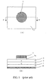
- FIG.1 shows a conventional LED structure.
- FIG. 1A is the top view
- FIG. 1B is the cross sectional view of AA'.
- a substrate 1 normally is n-type GaAs, GaP or GaN
- n-type semiconductor 2 and p-type semiconductor 3 are epitaxied to form a p-n junction.
- a thin layer of gold (Au) or AuGe alloy 5a forms a round shaped ohmic contact on the center of the chip, then aluminum (Al) bonding pad 7 is deposited for wire bonding.
- a metal electrode 10 is deposited on the backside of the substrate as the negative electrode. Gold wire connects the positive electrode to the aluminum-bonding pad 7.
- the electrode of a conventional LED on the center makes the electric field spreading uniformly around the chip, but gold and aluminum is opaqueness, light is blocking by the electrode too much if the electrode is large, but if too small, electric field would crowded in the center and the current density is increasing, this causes short life time of the LED, also in the center there will be a dark area which is obvious for near field observation; Also this electrode can not be used in overlap cascaded package.
- Another disadvantage of the convention electrode structure of a LED is that the lattice defect caused by cutting the chip along the scribe line. The electric field spreads from the electrode 7 via the p-type semiconductor to the substrate. Current will crowd easily at the lattice defect and form light spots, which also hurt the junction and cause decreasing of lifetime. So it is needed to develop an electrode structure for LEDs to get longer lifetime, suitable for overlap cascaded packaging.
- FIG.5 is the equivalent circuit of the bias method of FIG.4. Generally, a constant current source of 20mA is used as the power source as shown in FIG.5, but the voltage is different for the diodes of different colors.
- the control accuracy is difficult to obtain, and the design of the power control IC is complicated, more ever, for constant current, much heat generated and heat dispersion is not easy, it causes short life-time of the LED. In near field observation, three colors is still observed, full color can be observed only for far field observation, so it does not satisfy the need of the market.
- the object of the present invention is to provide an electrode structure of light emitted diode with decreasing electric field intensity around the periphery of the chip and increasing the lifetime of the LED.
- Another object of the present invention is to provide an electrode structure of light emitted diode with reflective metal around the chip to enhance the light emitting efficiency by reflecting the light emitted from the p-n junction to the reflective layer under the chip, and reflecting upward again. This makes the light emitted efficiently and there is no light emitted from the opaque region but only from the open window. If there is another LED with different color, overlap cascade bonded on the chip, the two colors may mix to form a mixed color such as white light if the two colors are complementary. No light without mixed is emitted alone and form a noise.
- Another object of the present invention is to provide an electrode structure of light emitted diode, using sapphire as the substrate, and the positive and negative electrodes are both on the front side.
- the transparent conductive or non-conductive layer on the backside of the substrate is used for die bonding only, and let the light comes from the bottom LED transmit upward to mix with the light of the upper LED to form a mixed light.
- Another object of the present invention is to provide an overlap cascaded packaging structure of a full color semiconductor LED to satisfy near field or far field display application.
- Yet another object of the present invention is to provide a light source with metal oxide transparent conductive layer or transparent non-conductive layer to die bond the multi-chip to form overlap cascaded packaging structure.
- the structure has good resolution and is satisfied for both near field or far field observation.
- the full color LED packaging structure for overlap bonding in cascade comprising: A substrate formed by GaAs, GaP, used as epitaxial substrate; A p-n junction of light emitted diode, epitaxied on said substrate; A silicon dioxide film and a reflective metal layer of gold germanium or gold alloy, is formed around the chip to decrease the electric field near the scribe line and formed an open window on the center such that light can emit from said window; A transparent conductive layer formed on said p-type semiconductor, said silicon dioxide layer and said reflective metal layer such that positive bias voltage is applied to the p-type semiconductor uniformly; A rectangular bonding pad formed by aluminum, aluminum alloy or gold, is formed on one side of the chip to be the positive bonding pad; A metal electrode formed on the bottom of said substrate to be a reflecting layer of light and a negative electrode, which may bond to a pc board or a lead frame.
- the silicon dioxide film and the reflective metal layer is replaced by etching a grove around the LED die.
- a transparent layer is formed on the bottom of said substrate to transmit the light from a bottom layer LED to mix with the light from an upper layer LED to form another color of light, and also used as a die bonding layer for overlap cascaded packaging.
- a full color LED packaging structure containing three-primary-color LED dice bond in cascade, by using a reflective metal layer and a transparent layer to overlap bond the red, blue and green LED dice in cascade on a bonding seat comprising: (a) a bonding seat, wherein a reflective metal layer is deposited and patterned to form a die bonding pad, a red LED positive bonding pad, a blue LED positive bonding pad, a green light positive bonding pad and a common negative bonding pad; (b) a first red LED die having a transparent conductive layer of positive electrode and a reflective metal layer of negative electrode, the red LED die is directly overlap bonded to the die bonding pad of the bonding seat; (c) a second blue LED die having a transparent conductive layer of positive and negative electrode, the blue LED die is directly overlap bonded in cascade by transparent non-conductive layer on the red LED die; (d) a third green LED die having a transparent conductive layer of positive and negative electrode, the green LED die is
- Yet another aspect of the present invention provides a full color LED packaging structure containing a blue LED die on a yellow LED die in parallel side-by-side with another green LED die on a red LED die, the yellow LED die is bonded to a bonding seat and the blue LED die is overlap bonded in cascade to the yellow LED die, the red LED die is bonded to the bonding seat and the green LED die is overlap cascade bonded to the red LED die, comprising: (a) A bonding seat, wherein a reflective metal layer is deposited and patterned to form a die bonding pad, a red LED positive bonding pad, a blue LED positive bonding pad, a yellow LED positive bonding pad, a green LED positive bonding pad and a common negative bonding pad; (b) A first yellow LED die having a transparent conductive layer of positive electrode and a reflective metal layer of negative electrode, the yellow LED die is directly overlap bond to the die bonding pad of the bonding seat; (c) A second blue LED die having a transparent conductive layer of positive electrode and a reflective
- the color, material and junction structure of the LED chip is not limited, any light emitted diode can use the electrode structure of the present invention.
- the electrode structure of the present invention is use in overlap cascaded structure packages of different color LED chips, by mixing two or three color light to have a different color light or white light.
- FIG.6 shows the electrode structure of a bottom LED die for overlap cascaded packaging of the first embodiment of the present invention.
- FIG.7 is the cross section along BB of FIG.6.
- Substrate 1 is III-V group compound semiconductor such as GaAs or GaP.
- n-type semiconductor 2 is formed by epitaxy on the substrate 1 (see the cross sectional view of FIG.7A and 7B).
- a p-type semiconductor 3 is expitaxied to form a p-n junction as the light emitted diode.
- the p-n junction may be double hetero structure or quantum well structure.
- An electrode structure of the present invention is formed on the p-type semiconductor.
- a silicon dioxide layer 4 of 200 ⁇ to 10000 ⁇ is deposited on the p-type semiconductor.
- a reflective metal layer 6 such as Cr, AuGe, Au or other gold alloys, with thickness of 200 ⁇ to 5000 ⁇ , the better of 500 ⁇ , is deposited on the oxide layer 4 and the semiconductor 3 .
- a first mask in lithography and etching process to etch away the oxide layer 4 and the reflective metal layer 6 to form an open window 8 and keep the silicon dioxide around the chip and under the bonding pad 7 .
- the width of the oxide layer 4 is 5-20 ⁇ m around the chip, but under the positive bonding pad 7 , the width of the oxide layer 4 is larger than the metal bonding pad 7 , so that after the electrode is formed, the metal electrode 5 , 6 , the silicon dioxide layer 4 and the p-type semiconductor 3 will form a capacitor which will decrease the electric field intensity around the scribe line. Under this weaker electric field, the lattice defects caused by scribing will not extraordinary emit lights to form light spots, and the lifetime of the LED chip will increase.
- a transparent conductive layer 5 with thickness of 200 ⁇ to 10000 ⁇ , the better of 500 ⁇ to 2000 ⁇ , is deposited on the p-type semiconductor 3 and silicon dioxide 4 to form ohmic contact with the p-type semiconductor 3.
- the thickness of the reflective metal layer 6 and the transparent conductive layer 5 is thin, so that avoid pilling when scribing into chips.
- bonding pad 7 is deposited on the reflective metal 6 and formed on one side of the chip (the right side of FIG.6 and FIG.7)
- the bonding pad 7 is a strip of Al, aluminum alloy, Au, or, gold alloys with thickness of 1000 ⁇ to 40000 ⁇ , the better of 10000 ⁇ , which is thicker than the transparent conductive layer 5 and the reflective metal layer 6 , for aluminum wire or gold wire boding.
- a metal negative electrode 10 is formed on the bottom of the substrate to be the negative electrode, which can be bonded to a PC board or a bonding seat of a lead-frame, also to be a reflective layer to reflect lights upward.
- the oxide under the bonding pad 7 forms a soft seat to absorb the stress of wire bonding without hurting the pn-junction and forming defects under the bonding pad 7 .
- FIG.7B shows another embodiment of the present invention.
- the electric field intensity along the scribe line can be formed by etching away a grove 9 of the transparent conductive layer 5 and the p-type semiconductor 3 around the die. This also decrease the electric field intensity along the scribe line, so that the lattice defect induced by scribing will not extraordinary emit lights to form light spots, and the lifetime of the LED chip will increase.
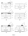
- Fig.8 shows the manufactory steps of the electrode of LED of the first embodiment of the present invention.
- n-type semiconductor 2 and p-type semiconductor 3 are epitaxied on substrate 1 to form a p-n junction
- silicon dioxide layer 4 with thickness of 200 ⁇ to 10000 ⁇ is deposited on the p-type semiconductor 3
- a reflective metal layer 6 of Cr, AuGe, Au or other gold alloy with thickness of 200 ⁇ to 5000 ⁇ , the better of 500 ⁇ is deposited
- lithography and etching step is performed with a first mask to remove the oxide layer 4 and the reflective metal layer 6 except that around the chip and that under the bonding pad 7
- the width of the oxide 4 is 5-20 ⁇ m around the chip, but under the positive bonding pad 7 , the width of the oxide layer 4 is larger than the bonding pad 7 to release the stress of wire bonding.
- a second mask, lithography and etching or lift-off process steps to form the bond pad 7 by using a second mask, lithography and etching or lift-off process steps to form the bond pad 7 .
- metal such as Al, aluminum alloy or gold is deposited on the bottom of the substrate to form a negative electrode 10 .
- FIG. 8D, E, and F show the manufacturing steps of the electrode of an LED with a grove around the die.
- n-type semiconductor 2 and p-type semiconductor 3 are epitaxied on substrate 1 to form a p-n junction
- a transparent conductive layer 5 with thickness of 200 ⁇ to 10000 ⁇ , the better of 500 ⁇ to 1000 ⁇ to be deposited is formed.
- lithography and etching step is performed with a first mask to etch a grove of the transparent conductive layer 5 and the p-type semiconductor 3 around the die.
- the width of transparent conductive layer and p-type semiconductor removed around the die is 10 ⁇ m to 50 ⁇ m.
- FIG.9A shows the top view of the structure of an LED die used for overlap cascaded packaging in accordance with one embodiment of the present invention.
- FIG. 9B is the cross sectional view along A-A line of the full color LED in FIG.9A.
- FIG.9C is the cross sectional view along B-B line of the full color LED in FIG.9A.
- a pn junction as the LED diode, but it is equivalent to use an np junction.
- a blue light (for example) LED chip 403 is made by epitaxy n-type InGaN 2 on a transparent sapphire substrate 1, then a p-type InGaN 3 is epitaxied on the n-type InGaN 2 to form a pn junction,
- the epitaxial is carry out by MOVPE(Metal Organic vapor Phase Epitaxy) technology.
- the negative bonding pad 901 is line up with the positive bonding pad 804 in one side of the chip.
- the reflective metal layer 6 prevent the light emit without mixing and conducting current around the chip to reduce the series resistance of the n-type InGaN, so that the driving voltage can be reduced.
- the thickness of the thin electrode layer 6 is very thin such that scribing along the scribe line will not damage the metal and the n-type crystal. Since in such structure, the p-n junction under the transparent conductive layer 5 keep away from the scribe line, so that the lattice defects induced by scribing will not extraordinary emit lights to form light spots, and the life time of the LED chip will increase, as shown in FIG.9C.
- FIG.10A shows the top view of the structure of an LED die used for overlap cascaded packaging in accordance with one embodiment of the present invention.
- the structure is the same as in FIG.9A except that the metal strip of positive electrode 804 is on the opposite site of the negative electrode 901.
- FIG 10B is the cross sectional view along A-A line of FIG. 10A.
- the strip electrode can be made as a square for saving chip area.
- the LED dice used in this invention can be made with different type of material.
- the dice can be made by conventional method in accordance with the specification of this invention such as chip size, bias voltage, intensity, color and metal contact, etc.
- the dice should be tested and classified before packaging.
- a pc-board or lead-frame with reflective metal pattern on the pc-board for die bonding after the first chip is bond on the pc-board, a second chip is overlap and cascade bonded on the first chip. Bonding can be thermal, ultrasonic or transparent epoxy, polyimide or other transparent materials adhesion. A third chip is also over lap and cascade bonded on the second chip. Wire bond is then connected the positive electrode to the power source and the negative electrode to common ground.
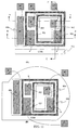
- FIG.11A and B shows the top view of an overlap cascaded three primary dice packaging structure of a full color LED suitable for near field observation in accordance with one embodiment of the present invention.
- FIG. 11A shows the plane view of a full color LED packaging on a pc board and
- FIG.11B shows the plane view of a full color LED packaging on a lead-frame.
- FIG. 12 is the cross section view along A-A line
- FIG. 13 is the cross section view along B-B line
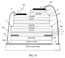
- FIG.14 is the cross section view along C-C line of the full color LED in FIG. 11A.
- a p-n junction as the LED diode, but it is equivalent to use an np junction.
- a red light LED chip 401 which is made by conventional method to form p-type InGaAIP/n-type GaAs (or GaP) pn junction, a layer of aluminum, copper or gold with thickness of 1000 ⁇ to 40000 ⁇ , the better of 2000 ⁇ to 10000 ⁇ , is sputtered or evaporated on the bottom of the chip, then a transparent conductive layer 5 with thickness of 200 ⁇ to 10000 ⁇ , the better of 500 ⁇ to 1000 ⁇ , is sputtered or evaporated to be the positive electrode. Then by using a first mask to perform lithography and etching away a grove of the transparent conductive layer 5 and the p-type InGaN layer 3 to expose the n-type InGaN 2.
- the negative bonding pad 901 is line up with the positive bonding pad 804 in one side of the chip.
- This layer also conducts current around the chip to reduce the series resistance of the n-type InGaN, so that the driving voltage can be reduced.
- the thickness of the thin electrode layer 6 is very thin such that scribing along the scribe line will not damage the metal and the n-type crystal.
- the size of the red light LED chip 401 is about 300 ⁇ m to 3000 ⁇ m.
- the red light LED 401 is then bonding to a pc-board or a lead-frame 405 by heating to the eutectic point of metal, for example, 450° C to 550° C, or by ultrasonic bonding or silver paste adhesion.
- a second blue light LED chip 403 is made by epitaxy n-type InGaN on a transparent sapphire substrate 805, then a p-type InGaN is epitaxied on the n-type InGaN to form a pn junction, The epitaxial is carry out by MOVPE technology. Then a transparent conductive layer 5 with thickness of 200 ⁇ to 10000 ⁇ , the better of 500 ⁇ to 1000 ⁇ , is sputtered or evaporated to be the positive electrode.
- a thin electrode layer 6 of metal such as Cr, Au or Al with width of 5-20 ⁇ m, and thickness of 200 ⁇ to 10000 ⁇ the better of 500 ⁇ is deposited to be the negative conducting metal 6, also a thick metal strip 901 of aluminum, copper or gold with width of 50 ⁇ m to 200 ⁇ m, the better of 100 ⁇ m and thickness of 1000 ⁇ to 40000 ⁇ , the better of 10000 ⁇ is deposited be the negative bonding pad 901.
- the negative bonding pad 901 is line up with the positive bonding pad 804 in one side of the chip.
- a metal strip 804 of aluminum, copper or gold with width of 50 ⁇ m to 200 ⁇ m, the better of 100 ⁇ m and thickness of 1000 ⁇ to 40000 ⁇ , the better of 10000 ⁇ is deposited to be the positive bonding pad of the blue light LED chip.
- the reflective metal layer 6 prevent the mixed blue and red light emit without mixing with the green light and become noise signal, and also reflect the blue and red light to the reflective layer on the pc-board upward again to mix with the green light, so that the energy of the blue and red light can be used completely.
- This layer also conducts current around the chip to reduce the series resistance of the n-type InGaN, so that the driving voltage can be reduced.
- the thickness of the thin electrode layer 6 is very thin such that scribing along the scribe line will not damage the metal and the n-type crystal. Since in such structure, the p-n junction under the transparent conductive layer 5 keep away from the scribe line, so that the lattice defects induced by scribing will not extraordinary emit lights to form light spots, and the life time of the LED chip will increase, as shown in FIG. 11, FIG. 12 and FIG. 13.
- the size of the blue LED chip is about 250 ⁇ m to 2500 ⁇ m.
- the blue LED chip 403 is overlap cascade bonded to the red LED chip 401 by a layer of transparent but non-conductive material such as epoxy, polyimide or other transparent materials adhesion.
- a third green LED chip 402 is also made by epitaxy an n-type InGaN and p-type InGaN on a transparent sapphire substrate 805, which can be made by a traditional technology. Then a transparent conductive layer 5 with thickness of 200 ⁇ to 10000 ⁇ , the better of 500 ⁇ to 1000 ⁇ , is sputtered or evaporated to be the positive electrode. By using a first mask to perform lithography and etching away a grove of the transparent conductive layer 5 and the p-type InGaN layer 3 to expose the n-type InGaN 2.
- the negative bonding pad 902 is line up with the positive bonding pad 907 in one side of the chip.
- the reflective layer 902 and 907 reflect the blue and red light to prevent the mixed blue and red light emit without mixing with the green light to become noise signal, and also reflect the mixed blue and red light so that the blue and red light can be used completely,
- This layer also conducts current around the chip to reduce the series resistance of the n-type InGaN, so that the driving voltage can be reduced.
- the thickness of the thin electrode layer 6 is very thin such that scribing along the scribe line will not damage the metal and the n-type crystal.
- the size of the green LED chip 402 is about 200 ⁇ m to 2000 ⁇ m. Then the green LED chip 402 is overlap bonded in cascade to the blue LED 403 by a layer of transparent but non-conductive material such as epoxy, polyamide or other transparent materials adhesion, as shown in FIG.12, FIG. 13 and FIG. 14.
- Wire bond is then connect the red, blue and green LED positive bonding pad R+, B+ and G+ to the positive bonding pad of the red, blue and green light on the pc board or lead frame respectively, and the negative pad B-, G- of the blue and green LED to the common ground 701 on the pc-board or lead frame, as shown in FIG. 11 and FIG. 14.
- the full color LED is then sealed with transparent plastic material.
- the package of this embodiment is then completed.
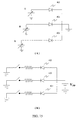
- the equivalent circuit is shown in FIG. 15A or B, where FIG. 15A is for common cathode of the electrical circuit and FIG.15B is for common anode of the electrical circuit.
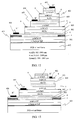
- FIG. 16 is the plane view.
- FIG.17 is the cross section along A-A line in FIG. 16.
- we do not use three primary color LEDs instead we use only two LEDs in overlap cascaded, then package in parallel side-by-side with another two LEDs in overlap cascaded.
- This structure satisfies far field observation. Refer to FIG. 17, which is using p-n junction dice in the present embodiment, but it is equivalent to use n-p junction dice.
- a red LED chip 401 made by epitaxing a p-type InGaAIP on an n-type GaAs substrate using a traditional technology.
- a transparent conductive layer 5 with thickness of 200 ⁇ to 5000 ⁇ , the better of 500 ⁇ to 1000 ⁇ is sputtered or evaporated to be the positive electrode.
- a first mask to perform lithography and etching away a grove of the transparent conductive layer 5 and the p-type InGaN layer 3 to expose the n-type InGaN 2.
- the negative bonding pad 902 is line up with the positive bonding pad 907 in one side of the chip.
- a strip layer of aluminum, copper or gold with width of 100 ⁇ m is deposited to be the positive bonding pad R+ 406 of the red LED,
- the metal layers 407, 902 and 6 prevent the red light emit forward alone to become noise signal, the reflected red light is then reflected upward by the reflective layer 801 and mixed with the green light above it.
- Conducting metal 6 also conducts current around the chip to reduce the series resistance of the n-type InGaN, so that the driving voltage can be reduced.
- the thickness of the thin electrode layer 6 is very thin such that scribing along the scribe line will not damage the metal and the n-type crystal.
- a reflective metal layer 801 with thickness of 1000 ⁇ to 20000 ⁇ , the better of 2000 ⁇ to 5000 ⁇ , is sputtered or evaporated.
- the size of the red LED is about 300 ⁇ m to 3000 ⁇ m.
- the red LED is then bond on the pc-board or lead frame by heating to the eutectic point of metal, for example 450 °C to 550 °C or by ultrasonic boding or silver-paste adhesion.
- the bottom metal 801 is connected to the common ground metal pattern 701 on the pc-board or the lead frame. Then prepare a second green light LED chip 402 which is made by traditional technology, for example, n-type InGaN / p-tpye InGaN on a sapphire 805.
- a transparent conductive layer 5 with thickness of 200 ⁇ to 5000 ⁇ , the better of 500 ⁇ to 1000 ⁇ is sputtered or evaporated to be the positive electrode.
- a first mask to perform lithography and etching away a grove of the transparent conductive layer 5 and the p-type InGaN layer 3 to expose the n-type InGaN 2.
- a strip of positive bonding pad G+ 407 with width of 100 ⁇ m is deposited and patterned on one side to be the positive bonding pad of the green light.
- the negative bonding pad 902 is line up with the positive bonding pad 407 in one side of the chip.
- the metal layer 902, 407 and 6 are used to reflect the red light back to the reflective layer 801 on the pc-board 405 and reflect upward again to mix with the green light, which can save energy, as shown in FIG. 16 and FIG.17.
- the green LED 402 is then overlap cascade bonded on the red LED chip 401 by transparent but non-conductive material such as epoxy, polyimide or other transparent materials adhesion.
- the size of the green LED is about 250 ⁇ m to 2500 ⁇ m.
- the yellow LED chip 131 and the blue LED 403 is overlap cascade bonded with the same method as that of the red LED chip and the green LED chip in parallel side-by-side as close as possible to the red and green LED, as shown in FIG. 16 and FIG. 17.
- the size of the yellow LED chip 131 is about 300 ⁇ m to 3000 ⁇ m.
- the size of the blue LED chip is about 250 ⁇ m to 2500 ⁇ m.
- the full color LED is then sealed with transparent plastic material.
- the equivalent circuit is shown in FIG. 19 for common cathode of p-n junction dice, it is value to notice that in this embodiment, different color is obtained by change the bias of each color to change the current and thus different light intensities are mixed to form different colors as shown in the chromaticity in FIG 2. In this case, along line A-B (yellow to blue) and C-D (red to green), we can adjust the intensity to obtain any color, including white light.
- Another embodiment of an overlap cascaded packaging structure full color LED according to the present invention is by using of the left part (the yellow and blue light LED chips in overlap cascaded package) or the right part (the red and green LED chips in overlap cascaded package) independently. By adjusting the bias of each LED and with a constant current to obtain a white light LED luminescence or a full color LED.
- the third embodiment does not limit to overlap cascaded package of the yellow and blue LED chips or the red and green LED chips, any two complementary color with which obtain a white light after mixed can be used.
- the materials used to fabricate the red, green, blue and yellow LEDs are not limited to the above materials, the structure of the diode is not limited to p-n junction structure, those advance technology such as quantum well structure can be used.
Landscapes
- Led Devices (AREA)
- Led Device Packages (AREA)
Priority Applications (1)
| Application Number | Priority Date | Filing Date | Title |
|---|---|---|---|
| EP03012081A EP1482566A3 (de) | 2003-05-28 | 2003-05-28 | Elektrodenstruktur für Leuchtdiode und Vollfarbenleuchtdiode durch kaskadiertes überlappendes Die-Bonding |
Applications Claiming Priority (1)
| Application Number | Priority Date | Filing Date | Title |
|---|---|---|---|
| EP03012081A EP1482566A3 (de) | 2003-05-28 | 2003-05-28 | Elektrodenstruktur für Leuchtdiode und Vollfarbenleuchtdiode durch kaskadiertes überlappendes Die-Bonding |
Publications (2)
| Publication Number | Publication Date |
|---|---|
| EP1482566A2 true EP1482566A2 (de) | 2004-12-01 |
| EP1482566A3 EP1482566A3 (de) | 2004-12-08 |
Family
ID=33104104
Family Applications (1)
| Application Number | Title | Priority Date | Filing Date |
|---|---|---|---|
| EP03012081A Withdrawn EP1482566A3 (de) | 2003-05-28 | 2003-05-28 | Elektrodenstruktur für Leuchtdiode und Vollfarbenleuchtdiode durch kaskadiertes überlappendes Die-Bonding |
Country Status (1)
| Country | Link |
|---|---|
| EP (1) | EP1482566A3 (de) |
Cited By (24)
| Publication number | Priority date | Publication date | Assignee | Title |
|---|---|---|---|---|
| DE102004056705A1 (de) * | 2004-09-30 | 2006-04-06 | Osram Opto Semiconductors Gmbh | Lumineszenzdiodenanordnung und Verfahren zur Überwachung von Lumineszenzdiodenchips |
| KR100726137B1 (ko) * | 2005-12-16 | 2007-06-12 | 루미마이크로 주식회사 | 금속 재질의 반사면을 형성하는 백색 발광소자의 제조방법 |
| EP2383804A1 (de) * | 2010-04-28 | 2011-11-02 | LG Innotek Co., Ltd. | Lichtemittierende Vorrichtung, Gehäuse für lichtemittierende Vorrichtung und Beleuchtungssystem |
| EP2164117A3 (de) * | 2008-09-09 | 2013-12-04 | Toshiba Techno Center, Inc. | Lichtemittierende Vorrichtung mit verbesserten Elektrodenstrukturen |
| US8637891B2 (en) | 2008-09-09 | 2014-01-28 | Toshiba Techno Center Inc. | Light-emitting device with improved electrode structures |
| US9431576B2 (en) | 2012-09-14 | 2016-08-30 | Epistar Corporation | Lighting device |
| CN106206558A (zh) * | 2012-09-14 | 2016-12-07 | 晶元光电股份有限公司 | 具有改进的热耗散和光提取的高压led |
| CN105637641B (zh) * | 2014-07-30 | 2018-08-28 | 孙润光 | 一种红色无机发光二极管显示器件及其制作方法 |
| CN109244064A (zh) * | 2017-07-11 | 2019-01-18 | 三星电子株式会社 | 发光装置封装件 |
| CN110678985A (zh) * | 2018-01-03 | 2020-01-10 | 首尔伟傲世有限公司 | 用于显示器的堆叠和具有其的显示设备 |
| CN110770921A (zh) * | 2017-12-21 | 2020-02-07 | 首尔伟傲世有限公司 | 发光堆叠结构和具有所述发光堆叠结构的显示装置 |
| US20210351230A1 (en) | 2017-11-27 | 2021-11-11 | Seoul Viosys Co., Ltd. | Light emitting diode (led) stack for a display |
| US11282981B2 (en) | 2017-11-27 | 2022-03-22 | Seoul Viosys Co., Ltd. | Passivation covered light emitting unit stack |
| US11289461B2 (en) | 2017-12-05 | 2022-03-29 | Seoul Viosys Co., Ltd. | Light emitting device with LED stack for display and display apparatus having the same |
| US11289536B2 (en) | 2017-11-27 | 2022-03-29 | Seoul Viosys Co., Ltd. | Light emitting device having commonly connected LED sub-units |
| CN114730815A (zh) * | 2019-09-11 | 2022-07-08 | 上海显耀显示科技有限公司 | 制造多色发光像素单元的方法 |
| CN114967231A (zh) * | 2022-05-16 | 2022-08-30 | 高创(苏州)电子有限公司 | 发光组件、背光模组及其驱动方法、显示装置 |
| US11522008B2 (en) | 2018-01-02 | 2022-12-06 | Seoul Viosys Co., Ltd. | Display device having light emitting stacked structure |
| US11527519B2 (en) | 2017-11-27 | 2022-12-13 | Seoul Viosys Co., Ltd. | LED unit for display and display apparatus having the same |
| US11527513B2 (en) | 2017-12-20 | 2022-12-13 | Seoul Viosys Co., Ltd. | LED unit for display and display apparatus having the same |
| US11552061B2 (en) | 2017-12-22 | 2023-01-10 | Seoul Viosys Co., Ltd. | Light emitting device with LED stack for display and display apparatus having the same |
| US11804512B2 (en) | 2017-12-14 | 2023-10-31 | Seoul Viosys Co., Ltd. | Light emitting stacked structure and display device having the same |
| WO2024130720A1 (en) * | 2022-12-23 | 2024-06-27 | Jade Bird Display (shanghai) Limited | Micro led structure and full color micro led panel |
| US12100696B2 (en) | 2017-11-27 | 2024-09-24 | Seoul Viosys Co., Ltd. | Light emitting diode for display and display apparatus having the same |
Family Cites Families (9)
| Publication number | Priority date | Publication date | Assignee | Title |
|---|---|---|---|---|
| JP2666228B2 (ja) * | 1991-10-30 | 1997-10-22 | 豊田合成株式会社 | 窒化ガリウム系化合物半導体発光素子 |
| EP1959506A2 (de) * | 1997-01-31 | 2008-08-20 | Matsushita Electric Industrial Co., Ltd. | Herstellungsverfahren für eine lichtemittierende Halbleitervorrichtung |
| JP3693468B2 (ja) * | 1997-07-23 | 2005-09-07 | シャープ株式会社 | 半導体発光素子 |
| JP3469484B2 (ja) * | 1998-12-24 | 2003-11-25 | 株式会社東芝 | 半導体発光素子およびその製造方法 |
| JP2001024220A (ja) * | 1999-07-13 | 2001-01-26 | Showa Denko Kk | Iii族窒化物半導体発光ダイオード |
| EP1275300A4 (de) * | 2000-04-21 | 2004-07-28 | Labosphere Inst | Drohvorrichtung |
| DE10044500A1 (de) * | 2000-09-08 | 2002-04-04 | Highlink Technology Corp Chupe | Licht emittierendes Verbindungshalbleiter-Bauteil und Verfahren zur Herstellung desselben |
| JP2003133590A (ja) * | 2001-10-25 | 2003-05-09 | Sharp Corp | 窒化ガリウム系化合物半導体発光素子及びその製造方法 |
| TW513821B (en) * | 2002-02-01 | 2002-12-11 | Hsiu-Hen Chang | Electrode structure of LED and manufacturing the same |
-
2003
- 2003-05-28 EP EP03012081A patent/EP1482566A3/de not_active Withdrawn
Cited By (63)
| Publication number | Priority date | Publication date | Assignee | Title |
|---|---|---|---|---|
| DE102004056705A1 (de) * | 2004-09-30 | 2006-04-06 | Osram Opto Semiconductors Gmbh | Lumineszenzdiodenanordnung und Verfahren zur Überwachung von Lumineszenzdiodenchips |
| DE102004056705B4 (de) * | 2004-09-30 | 2012-03-15 | Osram Opto Semiconductors Gmbh | Lumineszenzdiodenanordnung und Verfahren zur Überwachung von Lumineszenzdiodenchips |
| KR100726137B1 (ko) * | 2005-12-16 | 2007-06-12 | 루미마이크로 주식회사 | 금속 재질의 반사면을 형성하는 백색 발광소자의 제조방법 |
| EP2164117A3 (de) * | 2008-09-09 | 2013-12-04 | Toshiba Techno Center, Inc. | Lichtemittierende Vorrichtung mit verbesserten Elektrodenstrukturen |
| US8637891B2 (en) | 2008-09-09 | 2014-01-28 | Toshiba Techno Center Inc. | Light-emitting device with improved electrode structures |
| US9324915B2 (en) | 2008-09-09 | 2016-04-26 | Kabushiki Kaisha Toshiba | Light-emitting device with improved electrode structures |
| EP2383804A1 (de) * | 2010-04-28 | 2011-11-02 | LG Innotek Co., Ltd. | Lichtemittierende Vorrichtung, Gehäuse für lichtemittierende Vorrichtung und Beleuchtungssystem |
| US8362514B2 (en) | 2010-04-28 | 2013-01-29 | Lg Innotek, Co., Ltd. | Vertical semiconductor light emitting device including a capacitor |
| US9431576B2 (en) | 2012-09-14 | 2016-08-30 | Epistar Corporation | Lighting device |
| CN106206558A (zh) * | 2012-09-14 | 2016-12-07 | 晶元光电股份有限公司 | 具有改进的热耗散和光提取的高压led |
| TWI566432B (zh) * | 2012-09-14 | 2017-01-11 | 晶元光電股份有限公司 | 照明裝置 |
| US9966366B2 (en) | 2012-09-14 | 2018-05-08 | Epistar Corporation | Lighting device |
| CN106206558B (zh) * | 2012-09-14 | 2019-04-09 | 晶元光电股份有限公司 | 具有改进的热耗散和光提取的高压led |
| CN105637641B (zh) * | 2014-07-30 | 2018-08-28 | 孙润光 | 一种红色无机发光二极管显示器件及其制作方法 |
| CN109244064A (zh) * | 2017-07-11 | 2019-01-18 | 三星电子株式会社 | 发光装置封装件 |
| CN109244064B (zh) * | 2017-07-11 | 2024-03-12 | 三星电子株式会社 | 发光装置封装件 |
| US12456716B2 (en) | 2017-11-27 | 2025-10-28 | Seoul Viosys Co., Ltd. | LED unit for display and display apparatus having the same |
| US12009384B2 (en) | 2017-11-27 | 2024-06-11 | Seoul Viosys Co., Ltd. | Light emitting diode (LED) stack for a display |
| US11610939B2 (en) | 2017-11-27 | 2023-03-21 | Seoul Viosys Co., Ltd. | Light emitting diode (LED) stack for a display |
| US11532664B2 (en) | 2017-11-27 | 2022-12-20 | Seoul Viosys Co., Ltd. | Light emitting diode (LED) stack for a display |
| US11563052B2 (en) | 2017-11-27 | 2023-01-24 | Seoul Viosys Co., Ltd. | Light emitting diode (LED) stack for a display |
| US12142602B2 (en) | 2017-11-27 | 2024-11-12 | Seoul Viosys Co., Ltd. | Light emitting diode for display and display apparatus having the same |
| US12494461B2 (en) | 2017-11-27 | 2025-12-09 | Seoul Viosys Co., Ltd. | Light emitting diode for display and display apparatus having the same |
| US20210351230A1 (en) | 2017-11-27 | 2021-11-11 | Seoul Viosys Co., Ltd. | Light emitting diode (led) stack for a display |
| US11282981B2 (en) | 2017-11-27 | 2022-03-22 | Seoul Viosys Co., Ltd. | Passivation covered light emitting unit stack |
| US11527519B2 (en) | 2017-11-27 | 2022-12-13 | Seoul Viosys Co., Ltd. | LED unit for display and display apparatus having the same |
| US11289536B2 (en) | 2017-11-27 | 2022-03-29 | Seoul Viosys Co., Ltd. | Light emitting device having commonly connected LED sub-units |
| US12100696B2 (en) | 2017-11-27 | 2024-09-24 | Seoul Viosys Co., Ltd. | Light emitting diode for display and display apparatus having the same |
| US12062684B2 (en) | 2017-11-27 | 2024-08-13 | Seoul Viosys Co., Ltd. | Light emitting diode (LED) stack for a display |
| US12550482B2 (en) | 2017-11-27 | 2026-02-10 | Seoul Viosys Co., Ltd. | Passivation covered light emitting unit stack |
| US11804511B2 (en) | 2017-12-05 | 2023-10-31 | Seoul Viosys Co., Ltd. | Light emitting device with LED stack for display and display apparatus having the same |
| US11289461B2 (en) | 2017-12-05 | 2022-03-29 | Seoul Viosys Co., Ltd. | Light emitting device with LED stack for display and display apparatus having the same |
| US12356760B2 (en) | 2017-12-05 | 2025-07-08 | Seoul Viosys Co., Ltd. | Light emitting device with LED stack for display and display apparatus having the same |
| US12274106B2 (en) | 2017-12-14 | 2025-04-08 | Seoul Viosys Co., Ltd. | Light emitting stacked structure including epitaxial layers connecting with electrodes and display device having the same |
| US11804512B2 (en) | 2017-12-14 | 2023-10-31 | Seoul Viosys Co., Ltd. | Light emitting stacked structure and display device having the same |
| US12107081B2 (en) | 2017-12-20 | 2024-10-01 | Seoul Viosys Co., Ltd. | LED unit for display and display apparatus having the same |
| US11552057B2 (en) | 2017-12-20 | 2023-01-10 | Seoul Viosys Co., Ltd. | LED unit for display and display apparatus having the same |
| US11527514B2 (en) | 2017-12-20 | 2022-12-13 | Seoul Viosys Co., Ltd. | LED unit for display and display apparatus having the same |
| US11527513B2 (en) | 2017-12-20 | 2022-12-13 | Seoul Viosys Co., Ltd. | LED unit for display and display apparatus having the same |
| CN110770921A (zh) * | 2017-12-21 | 2020-02-07 | 首尔伟傲世有限公司 | 发光堆叠结构和具有所述发光堆叠结构的显示装置 |
| US12183773B2 (en) | 2017-12-21 | 2024-12-31 | Seoul Viosys Co., Ltd. | Light emitting stacked structure and display device having the same |
| US12453232B2 (en) | 2017-12-21 | 2025-10-21 | Seoul Viosys Co., Ltd. | Lighting emitting stacked structure and display device having the same |
| JP2021508938A (ja) * | 2017-12-21 | 2021-03-11 | ソウル バイオシス カンパニー リミテッドSeoul Viosys Co.,Ltd. | 発光積層構造とこれを備えたディスプレイデバイス |
| US11973104B2 (en) | 2017-12-21 | 2024-04-30 | Seoul Viosys Co., Ltd. | Light emitting stacked structure and display device having the same |
| US11522006B2 (en) | 2017-12-21 | 2022-12-06 | Seoul Viosys Co., Ltd. | Light emitting stacked structure and display device having the same |
| US11756984B2 (en) | 2017-12-21 | 2023-09-12 | Seoul Viosys Co., Ltd. | Light emitting stacked structure and display device having the same |
| EP3729518A4 (de) * | 2017-12-21 | 2021-09-08 | Seoul Viosys Co., Ltd | Lichtemittierende gestapelte struktur und anzeigevorrichtung damit |
| US11552061B2 (en) | 2017-12-22 | 2023-01-10 | Seoul Viosys Co., Ltd. | Light emitting device with LED stack for display and display apparatus having the same |
| US12334482B2 (en) | 2017-12-22 | 2025-06-17 | Seoul Viosys Co., Ltd. | Light emitting device with LED stack for display and display apparatus having the same |
| US11522008B2 (en) | 2018-01-02 | 2022-12-06 | Seoul Viosys Co., Ltd. | Display device having light emitting stacked structure |
| USRE50439E1 (en) | 2018-01-02 | 2025-05-20 | Seoul Viosys Co., Ltd. | Display device having light emitting stacked structure |
| US12230666B2 (en) | 2018-01-02 | 2025-02-18 | Seoul Viosys Co., Ltd. | Display device having light emitting stacked structure |
| EP3735707A4 (de) * | 2018-01-03 | 2021-11-03 | Seoul Viosys Co., Ltd | Lichtemittierende vorrichtung mit led-stapel für anzeige und anzeigevorrichtung damit |
| US12255190B2 (en) | 2018-01-03 | 2025-03-18 | Seoul Viosys Co., Ltd. | Light emitting device with LED stack for display and display apparatus having the same |
| JP2021509766A (ja) * | 2018-01-03 | 2021-04-01 | ソウル バイオシス カンパニー リミテッドSeoul Viosys Co.,Ltd. | ディスプレイ用のledスタックを有する発光素子及びそれを有するディスプレイ装置 |
| US11923348B2 (en) | 2018-01-03 | 2024-03-05 | Seoul Viosys Co., Ltd. | Light emitting device with LED stack for display and display apparatus having the same |
| US11557577B2 (en) | 2018-01-03 | 2023-01-17 | Seoul Viosys Co., Ltd. | Light emitting device with LED stack for display and display apparatus having the same |
| CN111508937A (zh) * | 2018-01-03 | 2020-08-07 | 首尔伟傲世有限公司 | 用于显示器的发光二极管像素及显示设备 |
| CN111508936A (zh) * | 2018-01-03 | 2020-08-07 | 首尔伟傲世有限公司 | 用于显示器的发光二极管像素及显示设备 |
| CN110678985A (zh) * | 2018-01-03 | 2020-01-10 | 首尔伟傲世有限公司 | 用于显示器的堆叠和具有其的显示设备 |
| CN114730815A (zh) * | 2019-09-11 | 2022-07-08 | 上海显耀显示科技有限公司 | 制造多色发光像素单元的方法 |
| CN114967231A (zh) * | 2022-05-16 | 2022-08-30 | 高创(苏州)电子有限公司 | 发光组件、背光模组及其驱动方法、显示装置 |
| WO2024130720A1 (en) * | 2022-12-23 | 2024-06-27 | Jade Bird Display (shanghai) Limited | Micro led structure and full color micro led panel |
Also Published As
| Publication number | Publication date |
|---|---|
| EP1482566A3 (de) | 2004-12-08 |
Similar Documents
| Publication | Publication Date | Title |
|---|---|---|
| US6563139B2 (en) | Package structure of full color LED form by overlap cascaded die bonding | |
| EP1482566A2 (de) | Elektrodenstruktur für Leuchtdiode und Vollfarbenleuchtdiode durch kaskadiertes überlappendes Die-Bonding | |
| US20030146445A1 (en) | Electrode structure of LED and manufacturing of the same | |
| KR100845856B1 (ko) | 발광 소자 패키지 및 그 제조방법 | |
| TWI892185B (zh) | 發光元件 | |
| JP3065258B2 (ja) | 発光装置及びそれを用いた表示装置 | |
| JP2900928B2 (ja) | 発光ダイオード | |
| US11239394B2 (en) | Semiconductor device and display device including the same | |
| KR100491314B1 (ko) | 발광장치 | |
| CN102214651B (zh) | 一种led像素单元器件结构及其制备方法 | |
| US7064354B2 (en) | Color mixing light emitting diode | |
| US9281454B2 (en) | Thin film light emitting diode | |
| CN102214650B (zh) | 一种led像素单元器件结构及其制备方法 | |
| US20070228386A1 (en) | Wire-bonding free packaging structure of light emitted diode | |
| JP2003197968A (ja) | 透明導電層及び反射層で直接結合されたチップの積み重ねによるフルカラー発光ダイオード光源のパッケージ構造 | |
| JP3476611B2 (ja) | 多色発光素子及びそれを用いた表示装置 | |
| US20050189551A1 (en) | High power and high brightness white LED assemblies and method for mass production of the same | |
| JP2000294831A (ja) | 半導体発光装置、半導体発光装置アレイ、フォトセンサおよびフォトセンサアレイ | |
| US20250169238A1 (en) | Semiconductor light-emitting device and semiconductor light-emitting component | |
| JPH0710003B2 (ja) | 混色発光半導体素子 | |
| JP2001217461A (ja) | 複合発光素子 | |
| JP2002158378A (ja) | 発光ダイオード | |
| US20020180345A1 (en) | Package structure containing two LEDs | |
| EP1469516A1 (de) | Weisslichtemittierende Halbleitervorrichtung mit mehreren Leuchtdioden-Chips | |
| JP2007258326A (ja) | 発光素子 |
Legal Events
| Date | Code | Title | Description |
|---|---|---|---|
| PUAI | Public reference made under article 153(3) epc to a published international application that has entered the european phase |
Free format text: ORIGINAL CODE: 0009012 |
|
| PUAL | Search report despatched |
Free format text: ORIGINAL CODE: 0009013 |
|
| AK | Designated contracting states |
Kind code of ref document: A2 Designated state(s): AT BE BG CH CY CZ DE DK EE ES FI FR GB GR HU IE IT LI LU MC NL PT RO SE SI SK TR |
|
| AX | Request for extension of the european patent |
Extension state: AL LT LV MK |
|
| AK | Designated contracting states |
Kind code of ref document: A3 Designated state(s): AT BE BG CH CY CZ DE DK EE ES FI FR GB GR HU IE IT LI LU MC NL PT RO SE SI SK TR |
|
| AX | Request for extension of the european patent |
Extension state: AL LT LV MK |
|
| AKX | Designation fees paid | ||
| REG | Reference to a national code |
Ref country code: DE Ref legal event code: 8566 |
|
| STAA | Information on the status of an ep patent application or granted ep patent |
Free format text: STATUS: THE APPLICATION IS DEEMED TO BE WITHDRAWN |
|
| 18D | Application deemed to be withdrawn |
Effective date: 20050609 |