EP1486331A1 - Piezoelectric actuator and fluid injection head having the same - Google Patents
Piezoelectric actuator and fluid injection head having the same Download PDFInfo
- Publication number
- EP1486331A1 EP1486331A1 EP03710386A EP03710386A EP1486331A1 EP 1486331 A1 EP1486331 A1 EP 1486331A1 EP 03710386 A EP03710386 A EP 03710386A EP 03710386 A EP03710386 A EP 03710386A EP 1486331 A1 EP1486331 A1 EP 1486331A1
- Authority
- EP
- European Patent Office
- Prior art keywords
- width
- piezoelectric
- common electrode
- piezoelectric body
- electrode
- Prior art date
- Legal status (The legal status is an assumption and is not a legal conclusion. Google has not performed a legal analysis and makes no representation as to the accuracy of the status listed.)
- Granted
Links
- 239000012530 fluid Substances 0.000 title 1
- 238000002347 injection Methods 0.000 title 1
- 239000007924 injection Substances 0.000 title 1
- 239000007788 liquid Substances 0.000 claims description 28
- 239000010410 layer Substances 0.000 description 38
- 230000015572 biosynthetic process Effects 0.000 description 19
- 239000000758 substrate Substances 0.000 description 16
- 238000004891 communication Methods 0.000 description 12
- 230000005684 electric field Effects 0.000 description 11
- 238000004519 manufacturing process Methods 0.000 description 10
- 239000000463 material Substances 0.000 description 10
- 230000001965 increasing effect Effects 0.000 description 9
- BASFCYQUMIYNBI-UHFFFAOYSA-N platinum Chemical compound [Pt] BASFCYQUMIYNBI-UHFFFAOYSA-N 0.000 description 6
- 239000002356 single layer Substances 0.000 description 6
- 230000008859 change Effects 0.000 description 5
- 239000007772 electrode material Substances 0.000 description 5
- 238000005192 partition Methods 0.000 description 5
- 239000002243 precursor Substances 0.000 description 5
- 239000000919 ceramic Substances 0.000 description 4
- 230000008602 contraction Effects 0.000 description 3
- 230000002708 enhancing effect Effects 0.000 description 3
- PCHJSUWPFVWCPO-UHFFFAOYSA-N gold Chemical compound [Au] PCHJSUWPFVWCPO-UHFFFAOYSA-N 0.000 description 3
- 239000010931 gold Substances 0.000 description 3
- 229910052737 gold Inorganic materials 0.000 description 3
- 229910052451 lead zirconate titanate Inorganic materials 0.000 description 3
- 239000004973 liquid crystal related substance Substances 0.000 description 3
- 229910052697 platinum Inorganic materials 0.000 description 3
- 230000009467 reduction Effects 0.000 description 3
- 230000004043 responsiveness Effects 0.000 description 3
- 238000005245 sintering Methods 0.000 description 3
- 238000000638 solvent extraction Methods 0.000 description 3
- 239000000126 substance Substances 0.000 description 3
- MCMNRKCIXSYSNV-UHFFFAOYSA-N Zirconium dioxide Chemical compound O=[Zr]=O MCMNRKCIXSYSNV-UHFFFAOYSA-N 0.000 description 2
- 239000000853 adhesive Substances 0.000 description 2
- 230000001070 adhesive effect Effects 0.000 description 2
- 238000004040 coloring Methods 0.000 description 2
- 230000007423 decrease Effects 0.000 description 2
- 230000001939 inductive effect Effects 0.000 description 2
- HFGPZNIAWCZYJU-UHFFFAOYSA-N lead zirconate titanate Chemical compound [O-2].[O-2].[O-2].[O-2].[O-2].[Ti+4].[Zr+4].[Pb+2] HFGPZNIAWCZYJU-UHFFFAOYSA-N 0.000 description 2
- 229910052751 metal Inorganic materials 0.000 description 2
- 239000002184 metal Substances 0.000 description 2
- 238000000034 method Methods 0.000 description 2
- 230000010355 oscillation Effects 0.000 description 2
- 239000011295 pitch Substances 0.000 description 2
- 230000003252 repetitive effect Effects 0.000 description 2
- 239000002002 slurry Substances 0.000 description 2
- PNEYBMLMFCGWSK-UHFFFAOYSA-N aluminium oxide Inorganic materials [O-2].[O-2].[O-2].[Al+3].[Al+3] PNEYBMLMFCGWSK-UHFFFAOYSA-N 0.000 description 1
- 239000011230 binding agent Substances 0.000 description 1
- 229910010293 ceramic material Inorganic materials 0.000 description 1
- 239000004020 conductor Substances 0.000 description 1
- 238000010276 construction Methods 0.000 description 1
- 230000008094 contradictory effect Effects 0.000 description 1
- 238000005520 cutting process Methods 0.000 description 1
- 230000003247 decreasing effect Effects 0.000 description 1
- 230000006866 deterioration Effects 0.000 description 1
- 230000002349 favourable effect Effects 0.000 description 1
- 230000006872 improvement Effects 0.000 description 1
- 239000002075 main ingredient Substances 0.000 description 1
- 239000011159 matrix material Substances 0.000 description 1
- 229910001092 metal group alloy Inorganic materials 0.000 description 1
- 239000000203 mixture Substances 0.000 description 1
- 230000010287 polarization Effects 0.000 description 1
- 238000003825 pressing Methods 0.000 description 1
- 238000007639 printing Methods 0.000 description 1
- 230000008569 process Effects 0.000 description 1
- 238000005086 pumping Methods 0.000 description 1
- 238000004080 punching Methods 0.000 description 1
- 230000004044 response Effects 0.000 description 1
- 230000002441 reversible effect Effects 0.000 description 1
- 238000007789 sealing Methods 0.000 description 1
- 238000009751 slip forming Methods 0.000 description 1
- 239000010935 stainless steel Substances 0.000 description 1
- 229910001220 stainless steel Inorganic materials 0.000 description 1
- 230000001131 transforming effect Effects 0.000 description 1
- 239000011800 void material Substances 0.000 description 1
Images



Classifications
-
- B—PERFORMING OPERATIONS; TRANSPORTING
- B41—PRINTING; LINING MACHINES; TYPEWRITERS; STAMPS
- B41J—TYPEWRITERS; SELECTIVE PRINTING MECHANISMS, i.e. MECHANISMS PRINTING OTHERWISE THAN FROM A FORME; CORRECTION OF TYPOGRAPHICAL ERRORS
- B41J2/00—Typewriters or selective printing mechanisms characterised by the printing or marking process for which they are designed
- B41J2/005—Typewriters or selective printing mechanisms characterised by the printing or marking process for which they are designed characterised by bringing liquid or particles selectively into contact with a printing material
- B41J2/01—Ink jet
- B41J2/135—Nozzles
- B41J2/16—Production of nozzles
- B41J2/1621—Manufacturing processes
- B41J2/1623—Manufacturing processes bonding and adhesion
-
- B—PERFORMING OPERATIONS; TRANSPORTING
- B41—PRINTING; LINING MACHINES; TYPEWRITERS; STAMPS
- B41J—TYPEWRITERS; SELECTIVE PRINTING MECHANISMS, i.e. MECHANISMS PRINTING OTHERWISE THAN FROM A FORME; CORRECTION OF TYPOGRAPHICAL ERRORS
- B41J2/00—Typewriters or selective printing mechanisms characterised by the printing or marking process for which they are designed
- B41J2/005—Typewriters or selective printing mechanisms characterised by the printing or marking process for which they are designed characterised by bringing liquid or particles selectively into contact with a printing material
- B41J2/01—Ink jet
- B41J2/135—Nozzles
- B41J2/14—Structure thereof only for on-demand ink jet heads
- B41J2/14201—Structure of print heads with piezoelectric elements
- B41J2/14233—Structure of print heads with piezoelectric elements of film type, deformed by bending and disposed on a diaphragm
-
- B—PERFORMING OPERATIONS; TRANSPORTING
- B41—PRINTING; LINING MACHINES; TYPEWRITERS; STAMPS
- B41J—TYPEWRITERS; SELECTIVE PRINTING MECHANISMS, i.e. MECHANISMS PRINTING OTHERWISE THAN FROM A FORME; CORRECTION OF TYPOGRAPHICAL ERRORS
- B41J2/00—Typewriters or selective printing mechanisms characterised by the printing or marking process for which they are designed
- B41J2/005—Typewriters or selective printing mechanisms characterised by the printing or marking process for which they are designed characterised by bringing liquid or particles selectively into contact with a printing material
- B41J2/01—Ink jet
- B41J2/135—Nozzles
- B41J2/16—Production of nozzles
- B41J2/1607—Production of print heads with piezoelectric elements
- B41J2/161—Production of print heads with piezoelectric elements of film type, deformed by bending and disposed on a diaphragm
-
- B—PERFORMING OPERATIONS; TRANSPORTING
- B41—PRINTING; LINING MACHINES; TYPEWRITERS; STAMPS
- B41J—TYPEWRITERS; SELECTIVE PRINTING MECHANISMS, i.e. MECHANISMS PRINTING OTHERWISE THAN FROM A FORME; CORRECTION OF TYPOGRAPHICAL ERRORS
- B41J2/00—Typewriters or selective printing mechanisms characterised by the printing or marking process for which they are designed
- B41J2/005—Typewriters or selective printing mechanisms characterised by the printing or marking process for which they are designed characterised by bringing liquid or particles selectively into contact with a printing material
- B41J2/01—Ink jet
- B41J2/135—Nozzles
- B41J2/16—Production of nozzles
- B41J2/1621—Manufacturing processes
- B41J2/1632—Manufacturing processes machining
-
- H—ELECTRICITY
- H10—SEMICONDUCTOR DEVICES; ELECTRIC SOLID-STATE DEVICES NOT OTHERWISE PROVIDED FOR
- H10N—ELECTRIC SOLID-STATE DEVICES NOT OTHERWISE PROVIDED FOR
- H10N30/00—Piezoelectric or electrostrictive devices
- H10N30/20—Piezoelectric or electrostrictive devices with electrical input and mechanical output, e.g. functioning as actuators or vibrators
- H10N30/204—Piezoelectric or electrostrictive devices with electrical input and mechanical output, e.g. functioning as actuators or vibrators using bending displacement, e.g. unimorph, bimorph or multimorph cantilever or membrane benders
- H10N30/2047—Membrane type
-
- B—PERFORMING OPERATIONS; TRANSPORTING
- B41—PRINTING; LINING MACHINES; TYPEWRITERS; STAMPS
- B41J—TYPEWRITERS; SELECTIVE PRINTING MECHANISMS, i.e. MECHANISMS PRINTING OTHERWISE THAN FROM A FORME; CORRECTION OF TYPOGRAPHICAL ERRORS
- B41J2/00—Typewriters or selective printing mechanisms characterised by the printing or marking process for which they are designed
- B41J2/005—Typewriters or selective printing mechanisms characterised by the printing or marking process for which they are designed characterised by bringing liquid or particles selectively into contact with a printing material
- B41J2/01—Ink jet
- B41J2/135—Nozzles
- B41J2/14—Structure thereof only for on-demand ink jet heads
- B41J2/14201—Structure of print heads with piezoelectric elements
- B41J2/14233—Structure of print heads with piezoelectric elements of film type, deformed by bending and disposed on a diaphragm
- B41J2002/14258—Multi layer thin film type piezoelectric element
-
- B—PERFORMING OPERATIONS; TRANSPORTING
- B41—PRINTING; LINING MACHINES; TYPEWRITERS; STAMPS
- B41J—TYPEWRITERS; SELECTIVE PRINTING MECHANISMS, i.e. MECHANISMS PRINTING OTHERWISE THAN FROM A FORME; CORRECTION OF TYPOGRAPHICAL ERRORS
- B41J2/00—Typewriters or selective printing mechanisms characterised by the printing or marking process for which they are designed
- B41J2/005—Typewriters or selective printing mechanisms characterised by the printing or marking process for which they are designed characterised by bringing liquid or particles selectively into contact with a printing material
- B41J2/01—Ink jet
- B41J2/135—Nozzles
- B41J2/14—Structure thereof only for on-demand ink jet heads
- B41J2002/14491—Electrical connection
-
- B—PERFORMING OPERATIONS; TRANSPORTING
- B41—PRINTING; LINING MACHINES; TYPEWRITERS; STAMPS
- B41J—TYPEWRITERS; SELECTIVE PRINTING MECHANISMS, i.e. MECHANISMS PRINTING OTHERWISE THAN FROM A FORME; CORRECTION OF TYPOGRAPHICAL ERRORS
- B41J2202/00—Embodiments of or processes related to ink-jet or thermal heads
- B41J2202/01—Embodiments of or processes related to ink-jet heads
- B41J2202/11—Embodiments of or processes related to ink-jet heads characterised by specific geometrical characteristics
Definitions
- the present invention relates to a piezoelectric actuator having a piezoelectric element, the element serving as a drive source, formed on the surface of a diaphragm.
- the present invention also relates to a liquid ejection head incorporating such a piezoelectric element provided on the surface of the diaphragm opposite a pressure chamber and changes the volume of the pressure chamber by the piezoelectric element.
- a piezoelectric element becomes deformed upon receipt of supplied electric energy and is widely used as, e.g., a liquid ejection head, a micropump, or a drive element for use with a sound-generating member (a speaker or the like).
- the liquid ejection head ejects droplets from nozzle orifices by inducing pressure fluctuations in liquid stored in a pressure chamber.
- the liquid ejection head includes a recording head used in an image recording apparatus such as a printer, a liquid-crystal ejection head used in manufacturing a liquid-crystal display, and a coloring material ejection head used in manufacturing a color filter.
- the micropump is a ultra-compact pump capable of pumping a trace amount of liquid and used at the time of, e.g., delivery of a trace amount of chemical.
- a piezoelectric actuator having a piezoelectric element provided on the surface of a diaphragm.
- the piezoelectric actuator is attached to a pressure chamber formation substrate having a void which serves as a pressure chamber, thereby partitioning a part of the pressure chamber with the diaphragm.
- a drive pulse is supplied to the piezoelectric element in order to deform the piezoelectric element and the diaphragm (e.g.; a deformation portion of the pressure chamber), thereby changing the volume of the pressure chamber.
- a piezoelectric element of multilayer structure has been proposed as an element which satisfies mutually contradictory characteristics; that is, the compliance of the deformation portion and the amount of deformation of the piezoelectric element.
- a piezoelectric element having a structure in which the piezoelectric layer is formed into a two-layer structure; that is, an upper piezoelectric body and a lower piezoelectric body, and in which a drive electrode (individual electrode) is formed at a boundary between the upper piezoelectric body and the lower piezoelectric body.
- a common electrode is formed on an exterior surface of the upper piezoelectric body and an exterior surface of the lower piezoelectric body (as described on, e.g., Japanese Patent Publication No. 2-289352A, page 6 and Fig. 5; and Japanese Patent Publication No. 10-34924A, page 5 and Fig. 9).
- the piezoelectric. element of multilayer structure has a drive electrode provided at a boundary between the upper piezoelectric body and the lower piezoelectric body, the respective layer piezoelectric bodies are provided with electric fields whose intensities are defined by intervals between the drive electrode and the respective common electrodes (i.e., the thicknesses of the respective layer piezoelectric bodies) and potential differences between the drive electrode and the respective common electrode.
- the piezoelectric element when compared with a piezoelectric element of a single layer structure having a single layer of piezoelectric body sandwiched between the common electrode and the drive electrode, the piezoelectric element can be deformed greatly with the same drive voltage as a conventional drive voltage even when the thickness of the entire piezoelectric element is increased slightly and the compliance of the deformation portion is reduced.
- a piezoelectric actuator comprising:
- the linearity of deformation of an upper piezoelectric layer can be made preferable.
- deformation of the piezoelectric element which arises at the time of driving operation, can be controlled more precisely, thereby enhancing stability of deformation.
- the drive electrode has a first width in a first direction
- the second piezoelectric layer has a second width in the first direction which is wider than the first width, so as to cover both ends in the first direction :of the drive electrode.
- the drive electrode remains embedded in the piezoelectric body. Hence, occurrence of atmospheric discharge can be prevented, thereby preventing occurrence of faulty operation.
- the configuration prevents occurrence of a failure, such as occurrence of a short circuit between a drive electrode and another electrode which would otherwise be caused during manufacturing operation or when the piezoelectric actuator is in use.
- a piezoelectric actuator comprising:
- the drive electrode has a third width in the first direction which is narrower than the second width such that both ends in the first direction of the drive electrode is covered by the second piezoelectric layer.
- a piezoelectric actuator comprising:
- a liquid ejection head comprising any one of the above piezoelectric actuators such that the vibration plate constitutes a part of a chamber communicated with a nozzle orifice from which a liquid droplet is ejected.
- the chamber has a first width in a first direction
- the second piezoelectric layer has a second width in the first direction wider than the first width
- the chamber has a first width in a first direction and the first piezoelectric layer has a second width in the first direction wider than the first width.
- the width of the drive electrode can be broadened to the greatest possible extent, and the amount of deformation of the piezoelectric element can be increased correspondingly.
- the embodiments will be described hereinbelow by reference to the accompanying drawings.
- a recording head a kind of liquid ejection head
- the recording head has a plurality of head main bodies 1 which are attached to a mount base 61.
- the head main body 1 is formed substantially from a flow passage unit 2 and an actuator unit 3.
- the flow passage unit 2 is fabricated from a supply port formation substrate 6 having formed therein through holes which are to act as ink supply ports 4, and through holes which are to constitute portions of nozzle communication ports 5; an ink chamber formation substrate 8 having formed therein through holes which are to act as a common ink chamber 7, and through holes which are to constitute the portions of the nozzle communication ports 5; and a nozzle plate 10 having formed therein nozzle orifices 9 oriented in a secondary scanning direction (i.e., a direction orthogonal to a primary scanning direction in which a recording head is to move).
- the supply port formation substrate 6, the ink chamber formation substrate 8, and the nozzle plate 10 are formed by pressing, for example, a stainless steel plate.
- the flow passage unit 2 is fabricated by placing the nozzle plate 10 on one surface of the ink chamber formation substrate 8 (e.g., a lower surface in the drawing) and the supply port formation substrate 6 on the other surface of the same (e.g., an upper surface in the drawing), and bonding together the supply port formation substrate 6, the ink chamber formation substrate 8, and the nozzle plate 10.
- the flow passage unit 2 is fabricated by bonding together the members 6, 8, and 10 by use of, e.g., a sheet-shaped adhesive.
- the nozzle orifices 9 are formed in a plurality of rows at predetermined pitches. Rows of nozzles 11 are formed from the plurality of nozzle orifices 9 arranged in rows. For example, a row of nozzles 11 is formed from 92 nozzle orifices 9. Two rows of nozzles 11 are formed side by side.
- the actuator unit 3 is a member also called a head chip.
- the actuator unit 3 comprises a pressure chamber formation substrate 13 having formed therein through holes (or voids) which are to constitute pressure chambers 12; a diaphragm 14 for partitioning portions of the respective pressure chambers 12; a cover member 16 having formed therein through holes which are to constitute portions of supply-side communication ports 15, and through holes which are to constitute portions of the nozzle communication ports 5; and a piezoelectric element 17 serving as a drive source.
- the pressure chamber formation substrate 13 and the cover member 16 preferably. assume a thickness of 50 ⁇ m or more, more preferably, 100 ⁇ m or more.
- the diaphragm 14 preferably assumes a thickness of 50 ⁇ m or less, more preferably, 3 to 12 ⁇ m.
- the diaphragm 14 and the piezoelectric element 17 constitute a piezoelectric actuator of the invention.
- the diaphragm 14 is a kind of support member on which the piezoelectric element 17 is to be provided.
- the actuator unit 3 is made by bonding the cover member 16 to one surface of the pressure chamber formation substrate 13 and the diaphragm 14 to the other surface of the same, and by forming the piezoelectric element 17 on the surface of the diaphragm 14.
- the pressure chamber formation substrate 13, the diaphragm 14, and the cover member 16 are made from ceramics, such as alumina or zirconia, by sintering.
- the pressure chamber formation substrate 13, the diaphragm 14, and the cover member 16 are bonded together in accordance with the following procedures.
- ceramic slurry is prepared from ceramic material, a binder, a liquid medium, or the like.
- a green sheet i.e., a sheet material which has not yet been sintered
- a common apparatus such as a doctor blade apparatus or a reverse roll coater.
- the green sheet is subjected to processing, such as cutting or punching, thereby forming required through holes.
- sheet-shaped precursors for the pressure chamber formation substrate 13, the diaphragm 14, and the cover member 16 are formed.
- the sheet-shaped precursors are laminated and sintered, thereby integrating the sheet-shaped precursors into a single sheet-shaped member.
- the respective sheet-shaped precursors are sintered integrally, special bonding operation is not required.
- a high sealing characteristic can also be achieved at joined surfaces of the respective sheet-shaped precursors.
- the pressure chambers 12 and the nozzle communication ports 5, which are equal in number to units, are formed in one sheet-shaped member.
- a plurality of actuator units (head chips) 3 are formed from one sheet-shaped member.
- a plurality of chip areas, which are to become single actuator units 3 are set in a matrix pattern within one sheet-shaped member.
- Required members, such as the piezoelectric element 17, are formed in each chip area.
- the sheet-shaped member (i.e., a ceramic sheet) on which the required members are formed is sliced for each chip area, thereby producing a plurality of actuator units 3.
- the pressure chamber 12 is a hollow section which is elongated in the direction orthogonal to the row of nozzles 11, and a plurality of pressure chambers 12 are formed so as to correspond to the nozzle orifices 9. Specifically, as shown in Fig. 2, the pressure chambers 12 are arranged in rows aligned with the row of nozzles. One end of each pressure chamber 12 is in communication with the corresponding nozzle orifice 9 by way of the nozzle communication port 5. The other end of the pressure chamber 12, on the side opposite the nozzle communication port 5, is in communication with the common ink chamber 7 by way of the supply-side communication port 15 and the ink supply port 4. A part of the pressure chamber 12 is partitioned by the diaphragm 14.
- the piezoelectric element 17 is a piezoelectric element of so-called flexural: oscillation mode and is provided, for each pressure chamber 12, on the surface of the diaphragm 14 opposite the pressure chamber 12.
- the width of the. piezoelectric element 17 is determined with reference to that of the pressure chamber 12, and the piezoelectric element 17 is somewhat greater in length than the pressure chamber 12. More specifically, the piezoelectric element 17 is formed so as to cover the pressure chamber 12 in the longitudinal direction thereof.
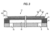
- the piezoelectric element 17 has a multilayer structure formed from a piezoelectric body layer 31, a common electrode 32, a drive electrode 33, and the like.
- the piezoelectric body layer 31 is sandwiched between the drive electrode 33 and the common electrode 32. The detailed structure of the piezoelectric element 17 will be described later in detail.
- a drive signal supply source (not shown) is electrically connected to the drive electrode 33.
- the common electrode 32 is controlled to a given earth potential.
- a drive signal is supplied to the drive electrode 33, an electric field whose intensity is related to a potential difference between the drive electrode 33 and the common electrode 32 develops. Since the electric field is imparted to the piezoelectric body layer 31, the piezoelectric body layer 31 becomes deformed in accordance with the intensity of the imparted electric field. More specifically, as the electric potential of the drive electrode 33 increases, the piezoelectric body layer 31 contracts in the direction orthogonal to the electric field, thereby deforming the diaphragm 14 such that the volume of the pressure chamber 12 is reduced. In contrast, as the electric potential of the drive electrode 33 decreases, the piezoelectric body layer 31 expands in the direction orthogonal to the electric field, thereby deforming the diaphragm 14 such that the volume of the pressure chamber 12 is increased.
- the actuator unit 3 and the flow passage unit 2 are joined.
- a sheet-shaped adhesive is interposed between the supply port formation substrate 6 and the cover member 16. In this state, pressure is applied to the actuator unit 3 toward the flow passage unit 2, whereupon the actuator unit 3 and the flow passage unit 2 are bonded together.
- a continuous ink flow passage is formed for each nozzle orifice 9 so as to extend from the common ink chamber 7 to the nozzle orifice 9 by way of the ink supply port 4, the supply-side communication port 15, the pressure chamber 12, and the nozzle communication port 5.
- the inside of the ink flow passage is filled with ink (a kind of liquid).
- ink a kind of liquid
- a corresponding pressure chamber 12 expands or contracts by deforming the piezoelectric element 17, thereby causing pressure fluctuations in the ink stored in the pressure chamber 12.
- the nozzle orifice 9 can be caused to eject an ink droplet.
- the pressure chamber 12 having a stationary volume is subjected to abrupt contraction after having been inflated, the pressure chamber 12 is filled with ink in association with inflation of the pressure chamber 12.
- the ink stored in the pressure chamber 12 is pressurized, whereupon an ink droplet is ejected.
- high-speed recording operation involves a necessity for ejecting a larger number of ink droplets within a short period of time.
- the compliance of the diaphragm 14 and that of the piezoelectric element 17 i.e., a deformed portion of the pressure chamber 12
- both elements partitioning the pressure chamber 12 and the amount of deformation of the piezoelectric element 17 must be taken into consideration. More specifically, as the compliance of the deformed portion becomes greater, responsiveness of the pressure chamber to deformation is deteriorated, thereby posing difficulty in driving the recording head at a high frequency. In contrast, as the compliance of the deformed portion becomes smaller, the deformed portion becomes more difficult to deform, whereupon the amount of contraction of the pressure chamber 12 becomes smaller and the volume of one ink droplet is also decreased.
- a piezoelectric element of flexural oscillation mode which has already become commercially practical
- a piezoelectric element of monolayer structure formed by interposing a single layer of piezoelectric body between a common electrode and a drive electrode.
- the piezoelectric element has a maximum response frequency of about 25 kHz and a maximum ink droplet volume of about 13 pL (picoliters).
- the compliance of the deformed portion is reduced by use of the piezoelectric element 17 of multilayer structure. Further, the structure of the piezoelectric element 17 is improved, thereby enabling efficient ejection of a required quantity of ink droplet while enhancing stability of deformation of the piezoelectric element 17. The following description explains this point.
- the piezoelectric body layer 31 is formed from an upper piezoelectric body (i.e., an outer piezoelectric body) 34 and a lower piezoelectric body (i.e., an inner piezoelectric body) 35, which are. stacked one over another.
- the common electrode 32 is formed from an upper common electrode (i.e., a common outer electrode) 36 and a lower common electrode (i.e., a common inner electrode) 37.
- the common electrode 32 and a drive electrode (individual electrodes) 33 constitute an electrode layer.
- the terms “upper (outer)” and “lower (inner)” denote positional relationships with reference to the diaphragm 14.
- the terms denote positional relationships with reference to the surface of the piezoelectric element 17 joined to the diaphragm 14 (which can also be referred to as an operating surface to be used for deforming the piezoelectric element 17, to thereby produce an output).
- the term “upper (outer)” denotes the surface of the piezoelectric element distant from the diaphragm 14, and the term “lower (inner)” denotes the surface of the same close to the diaphragm 14.
- the drive electrode 33 is formed at a boundary between the upper piezoelectric body 34 and the lower piezoelectric body 35.
- the lower common electrode 37 is formed between the lower piezoelectric body 35 and the diaphragm 14.
- the upper common electrode 36 is formed on the surface of the upper piezoelectric body 34 opposite the lower piezoelectric body 35.
- the piezoelectric element 17 has a multilayer structure comprising, in the order from the diaphragm 14, the lower common electrode 37, the lower piezoelectric body 35, the drive electrode 33, the upper piezoelectric body 34, and the upper common electrode 36.
- the thickness of the piezoelectric body layer 31 is equal to a total thickness of the upper piezoelectric body 34 and the lower piezoelectric body 35: that is, about 20 ⁇ m. Further, the total thickness of the piezoelectric element 17, including the common electrode 32, is about 23 ⁇ m.
- the total thickness of the conventional piezoelectric element 17 of monolayer structure is about 15 ⁇ m. Accordingly, as the thickness of the piezoelectric element 17 is increased, the compliance of the diaphragm 14 becomes smaller correspondingly.
- the upper common electrode 36 and the lower common electrode 37 are controlled to a given potential regardless of the drive signal.
- the upper common electrode 36 and the lower common electrode 37 are electrically connected together and controlled to the earth potential.
- the drive electrode 33 is electrically connected to the drive signal supply source as mentioned above and, hence, changes a potential in accordance with a supplied drive signal. Accordingly, supply of the drive signal induces an electric field between the drive electrode 33 and the upper common electrode 36, and between the drive electrode 33 and the lower common electrode 37, wherein the electric fields are opposite in direction to each other.
- Various conductors e.g., a single metal substance, a metal alloy, or a mixture consisting of electrically insulating ceramics and metal, are selected as materials which constitute the electrodes 33, 36, and 37.
- the materials are required not to cause any deterioration at a sintering temperature.
- gold is used for the upper common electrode 36
- platinum is used for the lower common electrode 37 and the drive electrode 33.
- the upper piezoelectric body 34 and the lower piezoelectric body 35 are formed from piezoelectric material containing, e.g., lead zirconate titanate (PZT) as the main ingredient.
- PZT lead zirconate titanate
- the direction of polarization of the upper piezoelectric body 34 is opposite that of the lower piezoelectric body 35. Therefore, when the drive signal is applied to the upper piezoelectric body 34 and the lower piezoelectric body 35, the substances expand and contract in the same direction and can become deformed without any problem.
- the upper piezoelectric body 34 and the lower piezoelectric body 35 deform the diaphragm 14 such that the volume of the pressure chamber 12 is reduced with an increase in the potential of the drive electrode 33 and such that the volume of the pressure chamber 12 is increased with a decrease in the potential of the drive electrode 33.
- the thickness tp1 of the upper piezoelectric body 34 is made greater than the thickness tp2 of the lower piezoelectric body 35.
- the thickness tp1 of the upper piezoelectric body 34 is set to 12 ⁇ m
- the thickness tp2 of the lower piezoelectric body 35 is set to 8 ⁇ m.
- the linearity of deformation of the upper piezoelectric body 34 that is, a characteristic of the upper piezoelectric body capable of tracking a change in the drive signal
- the piezoelectric element 17 can be deformed into a designed shape.
- the volume of the pressure chamber 12 can be controlled more precisely, and therefore the piezoelectric element is suitable for an application involving more elaborate control of an ejection characteristic; for example, an application to high-quality printing.
- the upper piezoelectric body 34 is provided so as to be wider than the drive electrode 33.
- the upper piezoelectric body 34 covers the entire width of the drive electrode 33 in a continuous manner. This is intended for preventing occurrence of a failure, such as atmospheric discharge or the like.
- an interval between the drive electrode 33 and the upper common electrode 36 and an interval between the drive electrode 33 and the lower common electrode 37 are very narrow, on the order of a few microns to tens of microns.
- Application of a voltage of the order of 30 V to 40 V is required to drive the respective layer piezoelectric bodies 34, 35.
- both end sections of the drive electrode 33 in a transverse direction thereof have appeared below the layer piezoelectric bodies 34, 35, atmospheric discharge may arise in a hot, humid atmosphere, possibly inducing faulty operation or a short circuit during manufacturing operation.
- the drive electrode 33 is coated with the upper piezoelectric body 34 as described in the embodiment, the drive electrode 33 is embedded in the piezoelectric body layer 31, thereby preventing occurrence of atmospheric discharge or faulty operation. Further, there can be prevented occurrence of a short circuit between the drive electrode 33 and another electrode (e.g., the upper common electrode 36 or the lower common electrode 37), which would otherwise be caused during manufacturing operation or when the device is in use.
- the piezoelectric body layer 31 (the lower piezoelectric body 35) is provided in an overhung manner in excess of side edges of the lower common electrode 37.
- the lower common electrode 37 is made narrower than the width wc of the pressure chamber 12 and is provided within the width of the pressure chamber.
- elastic regions Vc, Vc where only the diaphragm 14 is situated are formed at both ends of the diaphragm 14 in the transverse direction thereof. Provision of the elastic regions Vc renders the diaphragm 14 easier to deform, thus enhancing deformation efficiency.
- an electrode material which is thinner and more flexible than electrode materials of other electrodes (e.g., the drive electrode 33 and the lower common electrode 37), is used for the upper common electrode 36.
- the upper common electrode 36 is deformed to a greater extent than are other electrodes.
- the upper common electrode 36 is formed on the surface of the upper piezoelectric body 34 and hence becomes deformed to a greater extent than are the other electrodes.
- a material which is softer than those of the other electrodes is used for the upper common electrode 36, and/or the thickness of a material layer is made smaller.
- an electrode material having superior conductivity is preferably used so as to prevent occurrence of an excessive increase in electrical resistance, which would otherwise be caused when the thickness of the upper common electrode is reduced.
- the upper common electrode 36 is formed from gold, and the drive electrode 33 and the lower common electrode 37 are formed from platinum in the manner mentioned above.
- the lower common electrode 37 and the drive electrode 33 assume a thickness of 2 to 3 ⁇ m, whereas the upper common electrode 36 assumes about one-tenth that thickness (e.g., 0.3 ⁇ m).
- the upper common electrode 36 can be deformed so as to follow the piezoelectric element 17, thereby preventing a reduction in the amount of deformation of the piezoelectric element 17. Further, even when subjected to repeated deformation, the piezoelectric element 17 is not prone to failure, such as rupture. Moreover, an electric current can be caused to flow efficiently through the upper common electrode 36.
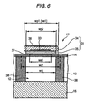
- a second embodiment shown in Fig. 6 is characterized in that the upper piezoelectric body 34 is formed so as to become wider than the inner dimension wc of the pressure chamber 12; that the upper common electrode 36 is formed so as to become wider than the lower common electrode 37; and that the upper common electrode 36 is formed over the entire width of the upper piezoelectric body 34 in a continuous manner.
- the width wp1 of the upper piezoelectric body 34 is formed so as to become wider than the inner dimension wc of the pressure chamber 12 and the width wp2 of the lower piezoelectric body 35 and narrower than an interval wc" (an interval wc" between partitions) between the centers of pressure chamber partitions 38 in a widthwise direction. Further, the center of the upper piezoelectric body 34 in the transverse direction is aligned with the center of the pressure chamber 12 in the transverse direction. In other words, the upper piezoelectric body 34 is formed inside of a width range defined between the centers of the pressure chamber partitions 38 in the thicknesswise direction thereof (i.e., inside of the range denoted by the partition interval wc"). As a result, a clearance is provided between adjacent upper piezoelectric bodies 34, and the piezoelectric elements 17 are provided without involvement of contact.
- the width (formation width) we1 of the upper common electrode 36 is caused to match the width wp1 of the upper piezoelectric body 34.
- the upper common electrode 36 is continuously formed from one end to the other end of the upper piezoelectric body 34 in the transverse direction thereof.
- gold which has superior conductivity and is a soft electrode material, is also used for the upper common electrode 36, and is formed into a very thin layer of about 0.3 ⁇ m.
- the recording head is identical in configuration with that described in connection with the previous embodiment. Hence, the same reference numerals are assigned to corresponding portions, and repetitive explanations are omitted.
- the width wp1 of the upper piezoelectric body 34 is wider than the inner width wc of the pressure chamber 12 in the transverse direction thereof, and the upper common electrode 36 is formed so as to cover the upper piezoelectric body 34 in a widthwise direction.
- An electric field developing between the drive electrode 33 and the upper common electrode 36 affects the entirety of the upper piezoelectric body 34 in a transverse direction. As a result, the entirety of the upper piezoelectric body 34 can be deformed in the transverse direction thereof.
- the upper piezoelectric body 34 is formed so as to become wider than the pressure chamber (i.e., wider than the inner dimension wc), the amount of deformation of the center section of the upper piezoelectric body 34 in the transverse direction thereof can be made greater than in the previous embodiment. Accordingly, the center of the diaphragm 14 in the transverse direction of the pressure chamber 12 can be greatly deformed, thereby efficiently transforming the deformation of the piezoelectric element 17 into a change in the volume of the pressure chamber 12.
- the width we1 of the upper common electrode 36 is made greater than the width we3 of the lower common electrode 37. Therefore, the range of deformation of the upper piezoelectric body 34 can be made wider than the range of deformation of the lower piezoelectric body 35.
- the center section of the upper piezoelectric body 34 in the transverse direction thereof can be deformed to a greater extent than can the center section of the lower piezoelectric body 35. Since the upper piezoelectric body 34 is more distant from the diaphragm 14 than is the lower piezoelectric body 35, deformation of the upper piezoelectric body 34 is amplified, thereby applying the amplified deformation to the diaphragm 14. Even in this regard, the center of the pressure chamber 12 in the transverse direction can be deformed greatly.
- the width of the drive electrode 33 can be broadened to the width of the lower piezoelectric body 35.
- an electric field developing between the electrodes can be made more intense than in the previous embodiment. Therefore, the piezoelectric element 17 can be deformed to as great an extent as possible, thus increasing a change in the volume of the pressure chamber 12 to as great a level as possible.
- the inner dimension wc of the pressure chamber 12 is 160 ⁇ m, and a pitch at which the pressure chambers 12 are formed (i.e., an interval corresponding to wc" shown in Fig. 6) assumes a value of 210 ⁇ m.
- the width wp1 of the upper piezoelectric body 34 can be increased to a maximum of about 1.3 times the inner dimension wc of the pressure chamber 12.
- the upper piezoelectric body 34 can be readily formed. Specifically, at the time of manufacture of the piezoelectric element 17, a paste of electrode material (e.g., platinum) which is to constitute a lower common electrode 37 is applied over the diaphragm 14 in a predetermined pattern by way of a mask, and the thus-applied paste is then sintered.
- electrode material e.g., platinum
- a paste of piezoelectric material (e.g., lead zirconate titanate) which is to constitute the lower piezoelectric body 35 is applied over the lower common electrode 37 in a predetermined pattern by way of the mask, and the thus-applied paste is then sintered.
- Application of a paste and sintering of the same are repetitively in the same manner, whereby the drive electrode 33, the upper piezoelectric body 34, and the upper common electrode 36 are formed sequentially.
- a pattern corresponding to the respective upper piezoelectric bodies 34 can be formed so as to become wider than the pattern of the lower piezoelectric body 35. Therefore, alignment of the mask used for forming the upper piezoelectric body 34 becomes relatively easy, thereby enabling an attempt to make a manufacturing operation efficient.
- the width wp1 of the upper piezoelectric body 34 is greater than the width wp2 of the lower piezoelectric body 35.
- the drive electrode 33 can be covered reliably with the upper piezoelectric body 34.
- a failure such as a short circuit between the drive electrode 33 and the common electrode 32, thereby preventing occurrence of a failure such as an atmospheric discharge.
- a third embodiment shown in Fig. 7 is characterized in that the lower piezoelectric body 34 is formed so as to become wider than the inner dimension wc of the pressure chamber 12.
- the width wp2 of the lower piezoelectric body 35 is formed so as to become wider than the inner dimension wc of the pressure chamber 12.
- the individual sections are provided in descending order from the widest section as follows. Specifically, the partition interval wc" is the widest, and the width wp1 of the upper piezoelectric body 34 and the width we1 of the upper common electrode 36 are the second widest.
- the width wp2 of the lower piezoelectric body 35 and the width we2 of the drive electrode 33 are the third widest.
- the inner dimension wc of the pressure chamber 12 is the fourth widest.
- the width we3 of the lower common electrode 37 is the smallest.
- the centers of the individual sections in the transverse direction thereof are aligned with the center of the pressure chamber 12 in the transverse direction thereof.
- the thickness tp1 of the upper piezoelectric body 34 is greater than the thickness tp2 of the lower piezoelectric body 35.
- the recording head is identical in configuration with that described in connection with the embodiment. Hence, the same reference numerals are assigned to corresponding portions, and repetitive explanations are omitted.
- the width we2 of the drive electrode 33 is matched with the width of the lower piezoelectric body 35 and set to the largest width. Therefore, electric fields developing between the electrodes can be made more intense, thereby enabling the greatest deformation of the piezoelectric element 17. As a result, ink droplets can be ejected efficiently.
- the upper common electrode 36 is formed so as to cover the upper piezoelectric body 34 in the transverse direction thereof. Hence, the amount of deformation of the center section of the upper piezoelectric body 34 in the transverse direction can be made greater than in the previous embodiment. Accordingly, even in the embodiment, deformation of the piezoelectric element 17 can be efficiently transformed into a change in the volume of the pressure chamber 12.
- the width wp1 of the upper piezoelectric body 34 is grater than the width wp2 of the lower piezoelectric body 35.
- the drive electrode 33 can be reliably covered with the upper piezoelectric body 34.
- occurrence of a failure such as a short circuit which would otherwise develop between the drive electrode 33 and the common electrode 32.
- occurrence of a failure due to an atmospheric discharge can also be prevented.
- the width wp2 of the lower piezoelectric body 35 is greater than the inner widthwise dimension wc of the pressure chamber 12.
- a deformation portion of the diaphragm 17 is covered with the piezoelectric element 17. Therefore, the compliance of that portion becomes smaller than that of the same portion achieved in the previous embodiment.
- the responsiveness of the piezoelectric element to deformation is improved.
- the piezoelectric element 17 can be driven at a higher frequency. Consequently; ejection of ink droplets at a higher frequency can be achieved.
- the width wp2 of the lower piezoelectric body 35 is set so as to becomes smaller than the width wp1 of the upper piezoelectric body 34.
- the width wp2 can be increased to the same width as the width wp1 of the upper piezoelectric body 34.
- a recording head which is a kind of liquid ejection head.
- the invention can also be applied to another liquid ejection head, such as a liquid-crystal ejection head or a coloring material ejection head, as well as to a piezoelectric actuator of the head.
- the invention can also be applied to a piezoelectric actuator for use with a micropump.
Landscapes
- Engineering & Computer Science (AREA)
- Manufacturing & Machinery (AREA)
- Particle Formation And Scattering Control In Inkjet Printers (AREA)
- Reciprocating Pumps (AREA)
- Organic Low-Molecular-Weight Compounds And Preparation Thereof (AREA)
Abstract
Description
In order to achieve the above object, according to the invention, there is provided a piezoelectric actuator, comprising:
Claims (12)
- A piezoelectric actuator, comprising:a vibration plate;a first common electrode, formed on the vibration plate and to be fixed at a predetermined potential;a first piezoelectric layer, laminated on the first common electrode and having a first thickness;a drive electrode, laminated on the first piezoelectric layer, to which a drive signal is supplied externally;a second piezoelectric layer, laminated on the drive electrode and having a second thickness thicker than the first thickness; anda second common electrode, laminated on the second piezoelectric layer and to be fixed at the predetermined potential.
- A piezoelectric actuator, comprising:a vibration plate;a first common electrode, formed on the vibration plate and to be fixed at a predetermined potential;a first piezoelectric layer, laminated on the first common electrode and having a first width in a first direction;a drive electrode, laminated on the first piezoelectric layer, to which a drive signal is supplied externally;a second piezoelectric layer, laminated on the drive electrode and having a second width in the first direction which is wider than the first width; anda second common electrode, laminated on the second piezoelectric layer and to be fixed at the predetermined potential.
- The piezoelectric actuator as set forth in claim 1, wherein the drive electrode has a first width in a first direction, and the second piezoelectric layer has a second width in the first direction which is wider than the first width, so as to cover both ends in the first direction of the drive electrode.
- The piezoelectric actuator as set forth in claim 2, wherein the drive electrode has a third width in the first direction which is narrower than the second width such that both ends in the first direction of the drive electrode is covered by the second piezoelectric layer.
- A piezoelectric actuator, comprising:a vibration plate;a first common electrode, formed on the vibration plate and to be fixed at a predetermined potential;a first piezoelectric layer, laminated on the first common electrode;a drive electrode, laminated on the first piezoelectric layer, to which a drive signal is supplied externally;a second piezoelectric layer, laminated on the drive electrode and having and having a first width in a first direction; anda second common electrode, laminated on the second piezoelectric layer and to be fixed at the predetermined potential, the second common electrode having a second width in the first direction which is substantially identical with the first width.
- A liquid ejection head, comprising the piezoelectric actuator as set forth in claim 1 such that the vibration plate constitutes a part of a chamber communicated with a nozzle orifice from which a liquid droplet is ejected.
- The liquid ejection head as set forth in claim 6, wherein the chamber has a first width in a first direction, and the second piezoelectric layer has a second width in the first direction wider than the first width.
- The liquid ejection head as set forth in claim 6, wherein the chamber has a first width in a first direction and the first piezoelectric layer has a second width in the first direction wider than the first width.
- A liquid ejection head, comprising the piezoelectric actuator as set forth in claim 2 such that the vibration plate constitutes a part of a chamber communicated with a nozzle orifice from which a liquid droplet is ejected.
- The liquid ejection head, as set forth in claim 9, wherein the chamber has a third width in the first direction which is narrower than the second width.
- The liquid ejection head as set forth in claim 9, wherein the chamber has a third width in the first direction which is narrower than the first width.
- A liquid ejection head, comprising the piezoelectric actuator as set forth in claim 5 such that the vibration plate constitutes a part of a chamber communicated with a nozzle orifice from which a liquid droplet is ejected.
Applications Claiming Priority (7)
| Application Number | Priority Date | Filing Date | Title |
|---|---|---|---|
| JP2002075087 | 2002-03-18 | ||
| JP2002075087 | 2002-03-18 | ||
| JP2002199178 | 2002-07-08 | ||
| JP2002199178 | 2002-07-08 | ||
| JP2003069235 | 2003-03-14 | ||
| JP2003069235A JP4100202B2 (en) | 2002-03-18 | 2003-03-14 | Piezoelectric actuator and liquid jet head |
| PCT/JP2003/003153 WO2003078166A1 (en) | 2002-03-18 | 2003-03-17 | Piezoelectric actuator and fluid injection head having the same |
Publications (3)
| Publication Number | Publication Date |
|---|---|
| EP1486331A1 true EP1486331A1 (en) | 2004-12-15 |
| EP1486331A4 EP1486331A4 (en) | 2009-05-06 |
| EP1486331B1 EP1486331B1 (en) | 2011-01-12 |
Family
ID=28046096
Family Applications (1)
| Application Number | Title | Priority Date | Filing Date |
|---|---|---|---|
| EP03710386A Expired - Lifetime EP1486331B1 (en) | 2002-03-18 | 2003-03-17 | Piezoelectric actuator and fluid injection head having the same |
Country Status (7)
| Country | Link |
|---|---|
| US (1) | US7265481B2 (en) |
| EP (1) | EP1486331B1 (en) |
| JP (1) | JP4100202B2 (en) |
| CN (2) | CN100540312C (en) |
| AT (1) | ATE495014T1 (en) |
| DE (1) | DE60335707D1 (en) |
| WO (1) | WO2003078166A1 (en) |
Cited By (3)
| Publication number | Priority date | Publication date | Assignee | Title |
|---|---|---|---|---|
| WO2005064701A3 (en) * | 2003-12-22 | 2006-03-02 | Koninkl Philips Electronics Nv | Electronic device |
| EP2371547A1 (en) * | 2010-03-30 | 2011-10-05 | Brother Kogyo Kabushiki Kaisha | Inkjet head, inkjet recording apparatus, and method of producing inkjet head |
| EP3002126A3 (en) * | 2014-10-02 | 2016-07-06 | Seiko Epson Corporation | Liquid ejecting head, liquid ejecting apparatus, and piezoelectric device |
Families Citing this family (12)
| Publication number | Priority date | Publication date | Assignee | Title |
|---|---|---|---|---|
| CN101611538A (en) * | 2007-01-12 | 2009-12-23 | 日本电气株式会社 | Piezoelectric actuators and electronics |
| US7768178B2 (en) | 2007-07-27 | 2010-08-03 | Fujifilm Corporation | Piezoelectric device, piezoelectric actuator, and liquid discharge device having piezoelectric films |
| JP4788764B2 (en) * | 2008-12-26 | 2011-10-05 | ブラザー工業株式会社 | Piezoelectric actuator and liquid transfer device |
| JP2013060554A (en) * | 2011-09-14 | 2013-04-04 | Seiko Epson Corp | Gel production apparatus and gel production method |
| EP2822297B1 (en) * | 2012-02-28 | 2020-01-08 | Kyocera Corporation | Piezoelectric vibration element, piezoelectric vibration apparatus, and mobile terminal |
| KR101952856B1 (en) * | 2013-11-25 | 2019-02-27 | 삼성전기주식회사 | Piezoelectric actuator |
| CN113230021A (en) * | 2015-01-12 | 2021-08-10 | 科达莱昂治疗公司 | Droplet delivery apparatus and method |
| US10241500B2 (en) * | 2015-08-10 | 2019-03-26 | Buerkert Werke Gmbh | Film transducer and actuator strip for a film transducer |
| DE202016106621U1 (en) | 2016-11-28 | 2017-02-27 | ANNAX GmbH | Double-sided screen with shared backlight |
| DE102016122922A1 (en) | 2016-11-28 | 2018-05-30 | ANNAX GmbH | Double-sided screen with shared backlight |
| CN108927234A (en) * | 2018-05-15 | 2018-12-04 | 西安交通大学 | It is a kind of to be impulsed the drop generating system of mechanism based on piezoelectricity |
| US11806191B2 (en) * | 2018-05-21 | 2023-11-07 | General Electric Company | Phased array transducers and wafer scale manufacturing for making the same |
Family Cites Families (20)
| Publication number | Priority date | Publication date | Assignee | Title |
|---|---|---|---|---|
| JP2952934B2 (en) | 1989-02-21 | 1999-09-27 | セイコーエプソン株式会社 | Liquid jet head, method of manufacturing the same, and liquid jet recording apparatus |
| JP2842448B2 (en) | 1989-07-11 | 1999-01-06 | 日本碍子株式会社 | Piezoelectric / electrostrictive film type actuator |
| DE69026765T2 (en) * | 1989-07-11 | 1996-10-24 | Ngk Insulators Ltd | Piezoelectric / electrostrictive actuator containing a piezoelectric / electrostrictive film |
| JPH08118630A (en) | 1994-10-26 | 1996-05-14 | Mita Ind Co Ltd | Printing head for ink jet printer and production thereof |
| JPH08118663A (en) | 1994-10-26 | 1996-05-14 | Mita Ind Co Ltd | Printing head for ink jet printer and production thereof |
| JP3366146B2 (en) * | 1995-03-06 | 2003-01-14 | セイコーエプソン株式会社 | Ink jet head |
| JP3484889B2 (en) | 1996-05-21 | 2004-01-06 | セイコーエプソン株式会社 | Piezoelectric vibrator unit, manufacturing method thereof, and ink jet recording head |
| JPH09277531A (en) * | 1996-04-18 | 1997-10-28 | Ricoh Co Ltd | Inkjet head |
| JP3666125B2 (en) * | 1996-06-05 | 2005-06-29 | 株式会社村田製作所 | Piezoelectric inkjet head |
| JPH115305A (en) | 1997-04-24 | 1999-01-12 | Matsushita Electric Ind Co Ltd | Liquid ejecting apparatus and manufacturing method thereof |
| JP3804247B2 (en) | 1998-01-29 | 2006-08-02 | ブラザー工業株式会社 | Method of joining members in a printer head |
| JP3379479B2 (en) * | 1998-07-01 | 2003-02-24 | セイコーエプソン株式会社 | Functional thin film, piezoelectric element, ink jet recording head, printer, method of manufacturing piezoelectric element and method of manufacturing ink jet recording head, |
| JP3451956B2 (en) | 1998-08-31 | 2003-09-29 | 松下電器産業株式会社 | Die collet for chip adsorption, chip bonding apparatus and bonding method |
| JP2000141647A (en) | 1998-11-10 | 2000-05-23 | Matsushita Electric Ind Co Ltd | Ink jet recording device |
| JP2000332313A (en) | 1999-05-21 | 2000-11-30 | Matsushita Electric Ind Co Ltd | Thin-film piezoelectric bimorph device and its application |
| JP2001024248A (en) | 1999-07-07 | 2001-01-26 | Samsung Electro Mech Co Ltd | Multi-layered piezoelectric/electrostrictive ceramic actuator and manufacture thereof by low-temperature baking |
| JP2001077438A (en) | 1999-09-07 | 2001-03-23 | Matsushita Electric Ind Co Ltd | Piezoelectric element, ink jet recording head, and manufacturing method thereof |
| JP3833070B2 (en) * | 2001-02-09 | 2006-10-11 | キヤノン株式会社 | Liquid ejecting head and manufacturing method |
| DE60238599D1 (en) | 2001-03-12 | 2011-01-27 | Ngk Insulators Ltd | TYPE-ACTUATOR WITH PIEZOELECTIVE / ELECTROSTRICTIVE FILM AND METHOD FOR THE PRODUCTION THEREOF |
| US7067961B2 (en) * | 2002-07-12 | 2006-06-27 | Ngk Insulators, Ltd. | Piezoelectric/electrostrictive film device, and manufacturing method of the device |
-
2003
- 2003-03-14 JP JP2003069235A patent/JP4100202B2/en not_active Expired - Fee Related
- 2003-03-17 US US10/498,600 patent/US7265481B2/en not_active Expired - Lifetime
- 2003-03-17 CN CNB2007100800079A patent/CN100540312C/en not_active Expired - Fee Related
- 2003-03-17 CN CNB038019574A patent/CN100333909C/en not_active Expired - Fee Related
- 2003-03-17 AT AT03710386T patent/ATE495014T1/en not_active IP Right Cessation
- 2003-03-17 WO PCT/JP2003/003153 patent/WO2003078166A1/en not_active Ceased
- 2003-03-17 EP EP03710386A patent/EP1486331B1/en not_active Expired - Lifetime
- 2003-03-17 DE DE60335707T patent/DE60335707D1/en not_active Expired - Lifetime
Cited By (7)
| Publication number | Priority date | Publication date | Assignee | Title |
|---|---|---|---|---|
| WO2005064701A3 (en) * | 2003-12-22 | 2006-03-02 | Koninkl Philips Electronics Nv | Electronic device |
| EP2371547A1 (en) * | 2010-03-30 | 2011-10-05 | Brother Kogyo Kabushiki Kaisha | Inkjet head, inkjet recording apparatus, and method of producing inkjet head |
| US8628175B2 (en) | 2010-03-30 | 2014-01-14 | Brother Kogyo Kabushiki Kaisha | Inkjet head, inkjet recording apparatus, and method of producing inkjet head |
| EP3002126A3 (en) * | 2014-10-02 | 2016-07-06 | Seiko Epson Corporation | Liquid ejecting head, liquid ejecting apparatus, and piezoelectric device |
| US9475289B2 (en) | 2014-10-02 | 2016-10-25 | Seiko Epson Corporation | Liquid ejecting head, liquid ejecting apparatus, and piezoelectric device |
| US9878538B2 (en) | 2014-10-02 | 2018-01-30 | Seiko Epson Corporation | Liquid ejecting head, liquid ejecting apparatus, and piezoelectric device |
| US9994021B2 (en) | 2014-10-02 | 2018-06-12 | Seiko Epson Corporation | Liquid ejecting head, liquid ejecting apparatus, and piezoelectric device |
Also Published As
| Publication number | Publication date |
|---|---|
| JP2004096069A (en) | 2004-03-25 |
| JP4100202B2 (en) | 2008-06-11 |
| CN100540312C (en) | 2009-09-16 |
| EP1486331B1 (en) | 2011-01-12 |
| EP1486331A4 (en) | 2009-05-06 |
| ATE495014T1 (en) | 2011-01-15 |
| US7265481B2 (en) | 2007-09-04 |
| WO2003078166A1 (en) | 2003-09-25 |
| DE60335707D1 (en) | 2011-02-24 |
| CN101024335A (en) | 2007-08-29 |
| US20050225205A1 (en) | 2005-10-13 |
| CN1612808A (en) | 2005-05-04 |
| CN100333909C (en) | 2007-08-29 |
Similar Documents
| Publication | Publication Date | Title |
|---|---|---|
| US7152290B2 (en) | Methods of manufacturing a piezoelectric actuator and a liquid jetting head | |
| US8182074B2 (en) | Liquid ejection head | |
| EP1486331B1 (en) | Piezoelectric actuator and fluid injection head having the same | |
| JP4305016B2 (en) | Piezoelectric actuator unit and liquid jet head using the same | |
| JPS63247051A (en) | Pulse droplet bonder and manufacture of pulse droplet bonder | |
| JP2004096070A (en) | Piezoelectric actuator and method for manufacturing the same, and liquid ejecting head and method for manufacturing the same | |
| US6918659B2 (en) | Piezoelectric element, piezoelectric actuator and liquid ejection head incorporating the same | |
| US6923528B2 (en) | Liquid-jet head and liquid-jet apparatus | |
| US6997547B2 (en) | Piezoelectric element, piezoelectric actuator and liquid jetting head incorporating the same | |
| JP4831051B2 (en) | Image recording apparatus, piezoelectric actuator, and liquid jet head | |
| JP4882963B2 (en) | Image recording apparatus, piezoelectric actuator, and liquid jet head | |
| JP4168682B2 (en) | Electrostrictive actuator | |
| JPH11300958A (en) | Ink jet recording head | |
| JPH07137259A (en) | Ink jet head and manufacture thereof | |
| JPH05261917A (en) | Ink jet type print head | |
| JP2003347615A (en) | Piezoelectric element and electrostrictive actuator | |
| JPH106495A (en) | Ink jet recording head and piezoelectric member |
Legal Events
| Date | Code | Title | Description |
|---|---|---|---|
| PUAI | Public reference made under article 153(3) epc to a published international application that has entered the european phase |
Free format text: ORIGINAL CODE: 0009012 |
|
| 17P | Request for examination filed |
Effective date: 20040528 |
|
| AK | Designated contracting states |
Kind code of ref document: A1 Designated state(s): AT BE BG CH CY CZ DE DK EE ES FI FR GB GR HU IE IT LI LU MC NL PT RO SE SI SK TR |
|
| AX | Request for extension of the european patent |
Extension state: AL LT LV MK |
|
| A4 | Supplementary search report drawn up and despatched |
Effective date: 20090403 |
|
| 17Q | First examination report despatched |
Effective date: 20090819 |
|
| GRAP | Despatch of communication of intention to grant a patent |
Free format text: ORIGINAL CODE: EPIDOSNIGR1 |
|
| GRAS | Grant fee paid |
Free format text: ORIGINAL CODE: EPIDOSNIGR3 |
|
| GRAA | (expected) grant |
Free format text: ORIGINAL CODE: 0009210 |
|
| AK | Designated contracting states |
Kind code of ref document: B1 Designated state(s): AT BE BG CH CY CZ DE DK EE ES FI FR GB GR HU IE IT LI LU MC NL PT RO SE SI SK TR |
|
| REG | Reference to a national code |
Ref country code: GB Ref legal event code: FG4D |
|
| REG | Reference to a national code |
Ref country code: CH Ref legal event code: EP |
|
| REG | Reference to a national code |
Ref country code: IE Ref legal event code: FG4D |
|
| REF | Corresponds to: |
Ref document number: 60335707 Country of ref document: DE Date of ref document: 20110224 Kind code of ref document: P |
|
| REG | Reference to a national code |
Ref country code: DE Ref legal event code: R096 Ref document number: 60335707 Country of ref document: DE Effective date: 20110224 |
|
| REG | Reference to a national code |
Ref country code: NL Ref legal event code: VDEP Effective date: 20110112 |
|
| PG25 | Lapsed in a contracting state [announced via postgrant information from national office to epo] |
Ref country code: PT Free format text: LAPSE BECAUSE OF FAILURE TO SUBMIT A TRANSLATION OF THE DESCRIPTION OR TO PAY THE FEE WITHIN THE PRESCRIBED TIME-LIMIT Effective date: 20110512 Ref country code: SE Free format text: LAPSE BECAUSE OF FAILURE TO SUBMIT A TRANSLATION OF THE DESCRIPTION OR TO PAY THE FEE WITHIN THE PRESCRIBED TIME-LIMIT Effective date: 20110112 Ref country code: ES Free format text: LAPSE BECAUSE OF FAILURE TO SUBMIT A TRANSLATION OF THE DESCRIPTION OR TO PAY THE FEE WITHIN THE PRESCRIBED TIME-LIMIT Effective date: 20110423 Ref country code: GR Free format text: LAPSE BECAUSE OF FAILURE TO SUBMIT A TRANSLATION OF THE DESCRIPTION OR TO PAY THE FEE WITHIN THE PRESCRIBED TIME-LIMIT Effective date: 20110413 |
|
| PG25 | Lapsed in a contracting state [announced via postgrant information from national office to epo] |
Ref country code: BG Free format text: LAPSE BECAUSE OF FAILURE TO SUBMIT A TRANSLATION OF THE DESCRIPTION OR TO PAY THE FEE WITHIN THE PRESCRIBED TIME-LIMIT Effective date: 20110412 Ref country code: SI Free format text: LAPSE BECAUSE OF FAILURE TO SUBMIT A TRANSLATION OF THE DESCRIPTION OR TO PAY THE FEE WITHIN THE PRESCRIBED TIME-LIMIT Effective date: 20110112 Ref country code: BE Free format text: LAPSE BECAUSE OF FAILURE TO SUBMIT A TRANSLATION OF THE DESCRIPTION OR TO PAY THE FEE WITHIN THE PRESCRIBED TIME-LIMIT Effective date: 20110112 Ref country code: NL Free format text: LAPSE BECAUSE OF FAILURE TO SUBMIT A TRANSLATION OF THE DESCRIPTION OR TO PAY THE FEE WITHIN THE PRESCRIBED TIME-LIMIT Effective date: 20110112 Ref country code: FI Free format text: LAPSE BECAUSE OF FAILURE TO SUBMIT A TRANSLATION OF THE DESCRIPTION OR TO PAY THE FEE WITHIN THE PRESCRIBED TIME-LIMIT Effective date: 20110112 Ref country code: CY Free format text: LAPSE BECAUSE OF FAILURE TO SUBMIT A TRANSLATION OF THE DESCRIPTION OR TO PAY THE FEE WITHIN THE PRESCRIBED TIME-LIMIT Effective date: 20110112 Ref country code: AT Free format text: LAPSE BECAUSE OF FAILURE TO SUBMIT A TRANSLATION OF THE DESCRIPTION OR TO PAY THE FEE WITHIN THE PRESCRIBED TIME-LIMIT Effective date: 20110112 |
|
| PG25 | Lapsed in a contracting state [announced via postgrant information from national office to epo] |
Ref country code: MC Free format text: LAPSE BECAUSE OF NON-PAYMENT OF DUE FEES Effective date: 20110331 Ref country code: EE Free format text: LAPSE BECAUSE OF FAILURE TO SUBMIT A TRANSLATION OF THE DESCRIPTION OR TO PAY THE FEE WITHIN THE PRESCRIBED TIME-LIMIT Effective date: 20110112 Ref country code: DK Free format text: LAPSE BECAUSE OF FAILURE TO SUBMIT A TRANSLATION OF THE DESCRIPTION OR TO PAY THE FEE WITHIN THE PRESCRIBED TIME-LIMIT Effective date: 20110112 |
|
| REG | Reference to a national code |
Ref country code: CH Ref legal event code: PL |
|
| PLBE | No opposition filed within time limit |
Free format text: ORIGINAL CODE: 0009261 |
|
| STAA | Information on the status of an ep patent application or granted ep patent |
Free format text: STATUS: NO OPPOSITION FILED WITHIN TIME LIMIT |
|
| PG25 | Lapsed in a contracting state [announced via postgrant information from national office to epo] |
Ref country code: RO Free format text: LAPSE BECAUSE OF FAILURE TO SUBMIT A TRANSLATION OF THE DESCRIPTION OR TO PAY THE FEE WITHIN THE PRESCRIBED TIME-LIMIT Effective date: 20110112 Ref country code: SK Free format text: LAPSE BECAUSE OF FAILURE TO SUBMIT A TRANSLATION OF THE DESCRIPTION OR TO PAY THE FEE WITHIN THE PRESCRIBED TIME-LIMIT Effective date: 20110112 Ref country code: CZ Free format text: LAPSE BECAUSE OF FAILURE TO SUBMIT A TRANSLATION OF THE DESCRIPTION OR TO PAY THE FEE WITHIN THE PRESCRIBED TIME-LIMIT Effective date: 20110112 |
|
| 26N | No opposition filed |
Effective date: 20111013 |
|
| PG25 | Lapsed in a contracting state [announced via postgrant information from national office to epo] |
Ref country code: IT Free format text: LAPSE BECAUSE OF FAILURE TO SUBMIT A TRANSLATION OF THE DESCRIPTION OR TO PAY THE FEE WITHIN THE PRESCRIBED TIME-LIMIT Effective date: 20110112 |
|
| REG | Reference to a national code |
Ref country code: IE Ref legal event code: MM4A |
|
| PG25 | Lapsed in a contracting state [announced via postgrant information from national office to epo] |
Ref country code: IE Free format text: LAPSE BECAUSE OF NON-PAYMENT OF DUE FEES Effective date: 20110317 Ref country code: LI Free format text: LAPSE BECAUSE OF NON-PAYMENT OF DUE FEES Effective date: 20110331 Ref country code: CH Free format text: LAPSE BECAUSE OF NON-PAYMENT OF DUE FEES Effective date: 20110331 |
|
| REG | Reference to a national code |
Ref country code: DE Ref legal event code: R097 Ref document number: 60335707 Country of ref document: DE Effective date: 20111013 |
|
| PG25 | Lapsed in a contracting state [announced via postgrant information from national office to epo] |
Ref country code: LU Free format text: LAPSE BECAUSE OF NON-PAYMENT OF DUE FEES Effective date: 20110317 |
|
| PG25 | Lapsed in a contracting state [announced via postgrant information from national office to epo] |
Ref country code: TR Free format text: LAPSE BECAUSE OF FAILURE TO SUBMIT A TRANSLATION OF THE DESCRIPTION OR TO PAY THE FEE WITHIN THE PRESCRIBED TIME-LIMIT Effective date: 20110112 |
|
| PG25 | Lapsed in a contracting state [announced via postgrant information from national office to epo] |
Ref country code: HU Free format text: LAPSE BECAUSE OF FAILURE TO SUBMIT A TRANSLATION OF THE DESCRIPTION OR TO PAY THE FEE WITHIN THE PRESCRIBED TIME-LIMIT Effective date: 20110112 |
|
| REG | Reference to a national code |
Ref country code: FR Ref legal event code: PLFP Year of fee payment: 14 |
|
| REG | Reference to a national code |
Ref country code: FR Ref legal event code: PLFP Year of fee payment: 15 |
|
| REG | Reference to a national code |
Ref country code: FR Ref legal event code: PLFP Year of fee payment: 16 |
|
| PGFP | Annual fee paid to national office [announced via postgrant information from national office to epo] |
Ref country code: DE Payment date: 20180306 Year of fee payment: 16 Ref country code: GB Payment date: 20180314 Year of fee payment: 16 |
|
| PGFP | Annual fee paid to national office [announced via postgrant information from national office to epo] |
Ref country code: FR Payment date: 20180223 Year of fee payment: 16 |
|
| REG | Reference to a national code |
Ref country code: DE Ref legal event code: R119 Ref document number: 60335707 Country of ref document: DE |
|
| GBPC | Gb: european patent ceased through non-payment of renewal fee |
Effective date: 20190317 |
|
| PG25 | Lapsed in a contracting state [announced via postgrant information from national office to epo] |
Ref country code: GB Free format text: LAPSE BECAUSE OF NON-PAYMENT OF DUE FEES Effective date: 20190317 Ref country code: DE Free format text: LAPSE BECAUSE OF NON-PAYMENT OF DUE FEES Effective date: 20191001 |
|
| PG25 | Lapsed in a contracting state [announced via postgrant information from national office to epo] |
Ref country code: FR Free format text: LAPSE BECAUSE OF NON-PAYMENT OF DUE FEES Effective date: 20190331 |