EP1486793A2 - Bobine supraconductrice de sonde r.f. pour la résonance magnétique - Google Patents
Bobine supraconductrice de sonde r.f. pour la résonance magnétique Download PDFInfo
- Publication number
- EP1486793A2 EP1486793A2 EP04012588A EP04012588A EP1486793A2 EP 1486793 A2 EP1486793 A2 EP 1486793A2 EP 04012588 A EP04012588 A EP 04012588A EP 04012588 A EP04012588 A EP 04012588A EP 1486793 A2 EP1486793 A2 EP 1486793A2
- Authority
- EP
- European Patent Office
- Prior art keywords
- coil
- thin film
- normal metal
- superconducting
- magnetic resonance
- Prior art date
- Legal status (The legal status is an assumption and is not a legal conclusion. Google has not performed a legal analysis and makes no representation as to the accuracy of the status listed.)
- Withdrawn
Links
Images







Classifications
-
- G—PHYSICS
- G01—MEASURING; TESTING
- G01R—MEASURING ELECTRIC VARIABLES; MEASURING MAGNETIC VARIABLES
- G01R33/00—Arrangements or instruments for measuring magnetic variables
- G01R33/20—Arrangements or instruments for measuring magnetic variables involving magnetic resonance
- G01R33/28—Details of apparatus provided for in groups G01R33/44 - G01R33/64
- G01R33/32—Excitation or detection systems, e.g. using radio frequency signals
- G01R33/34—Constructional details, e.g. resonators, specially adapted to MR
- G01R33/34046—Volume type coils, e.g. bird-cage coils; Quadrature bird-cage coils; Circularly polarised coils
- G01R33/34053—Solenoid coils; Toroidal coils
-
- G—PHYSICS
- G01—MEASURING; TESTING
- G01R—MEASURING ELECTRIC VARIABLES; MEASURING MAGNETIC VARIABLES
- G01R33/00—Arrangements or instruments for measuring magnetic variables
- G01R33/20—Arrangements or instruments for measuring magnetic variables involving magnetic resonance
- G01R33/28—Details of apparatus provided for in groups G01R33/44 - G01R33/64
- G01R33/32—Excitation or detection systems, e.g. using radio frequency signals
- G01R33/34—Constructional details, e.g. resonators, specially adapted to MR
- G01R33/345—Constructional details, e.g. resonators, specially adapted to MR of waveguide type
- G01R33/3453—Transverse electromagnetic [TEM] coils
- G01R33/3456—Stripline resonators
-
- G—PHYSICS
- G01—MEASURING; TESTING
- G01R—MEASURING ELECTRIC VARIABLES; MEASURING MAGNETIC VARIABLES
- G01R33/00—Arrangements or instruments for measuring magnetic variables
- G01R33/20—Arrangements or instruments for measuring magnetic variables involving magnetic resonance
- G01R33/28—Details of apparatus provided for in groups G01R33/44 - G01R33/64
- G01R33/32—Excitation or detection systems, e.g. using radio frequency signals
- G01R33/34—Constructional details, e.g. resonators, specially adapted to MR
- G01R33/34007—Manufacture of RF coils, e.g. using printed circuit board technology; additional hardware for providing mechanical support to the RF coil assembly or to part thereof, e.g. a support for moving the coil assembly relative to the remainder of the MR system
-
- G—PHYSICS
- G01—MEASURING; TESTING
- G01R—MEASURING ELECTRIC VARIABLES; MEASURING MAGNETIC VARIABLES
- G01R33/00—Arrangements or instruments for measuring magnetic variables
- G01R33/20—Arrangements or instruments for measuring magnetic variables involving magnetic resonance
- G01R33/28—Details of apparatus provided for in groups G01R33/44 - G01R33/64
- G01R33/32—Excitation or detection systems, e.g. using radio frequency signals
- G01R33/34—Constructional details, e.g. resonators, specially adapted to MR
- G01R33/34015—Temperature-controlled RF coils
- G01R33/34023—Superconducting RF coils
-
- G—PHYSICS
- G01—MEASURING; TESTING
- G01R—MEASURING ELECTRIC VARIABLES; MEASURING MAGNETIC VARIABLES
- G01R33/00—Arrangements or instruments for measuring magnetic variables
- G01R33/20—Arrangements or instruments for measuring magnetic variables involving magnetic resonance
- G01R33/28—Details of apparatus provided for in groups G01R33/44 - G01R33/64
- G01R33/32—Excitation or detection systems, e.g. using radio frequency signals
- G01R33/34—Constructional details, e.g. resonators, specially adapted to MR
- G01R33/34092—RF coils specially adapted for NMR spectrometers
Definitions
- the present invention relates to nuclear magnetic resonance equipment (hereinbelow, referred to as NMR equipment) and, more particularly, to NMR equipment characterized by the shape of a coil of a probe for transmitting a radio-frequency signal at a predetermined resonance frequency and/or receiving a free induction decay (FID) signal from a sample placed in a uniform magnetic field and by a structure for mounting.
- NMR equipment nuclear magnetic resonance equipment
- FID free induction decay
- NMR equipment capable of applying a radio-frequency signal of high resonance frequency to a sample in uniform high magnetic fields (B 0 ) in order to increase the resolution in nuclear magnetic resonance spectral (NMR spectral) has been developed.
- B 0 uniform high magnetic fields
- NMR spectral nuclear magnetic resonance spectral
- a superconducting magnet is generally used.
- high magnetic field NMR equipment for mainly analyzing the structure of protein is being developed.
- NMR equipment with magnetic field intensity of 21.6T and resonance frequency of 920 MHz is produced.
- a probe for receiving a free induction decay (FID) signal generated by a sample in response to the applied radio-frequency pulse signal is required to have high sensitivity.
- FID free induction decay
- the intensity of the FID signal is particularly low and it takes long time for measurement.
- Most noises of the probe occur due to electric resistance of the probe as a component of a resonator and depend on the temperature and surface resistance of a material.
- a probe coil and a preamplifier are disposed at a low temperature.
- a superconducting magnet having excellent uniformity in magnetic field intensity is realized by an integral-type solenoid magnet, and a variation with respect to a sample to be measured is as small as 10 -9 .
- NMR equipment having such a solenoid magnet the axial direction of a sample tube for introducing a sample to a magnetic field coincides with the axial direction of the solenoid magnet.
- a radio-frequency signal is applied perpendicular to the axial direction of the sample tube and the solenoid magnet. Consequently, a saddle coil and a bird-cage antenna are used for the probe.
- Japanese Unexamined Patent Publication No. Hei 11-133127 discloses the technique using a bird-cage antenna.
- the filling factor of the solenoid coil is higher than that of a saddle coil, a bird-cage coil, or a bird-cage antenna.
- a technique of making a solenoid coil of an oxide high-temperature superconductor is described in the above-described U.S. Patent No. 5,585,723.
- a flat donut-shaped ring (one coil part) is fabricated by a high-temperature superconducting thin film, and a part in the ring is trimmed, thereby forming a capacitor via a substrate.
- an LC resonator is formed. Since it is difficult to electrically connect coil parts, a solenoid coil cannot be formed by connecting a plurality of flat donut-shaped rings.
- a radio-frequency signal is applied to a sample by inductive coupling using mutual inductance of the coil parts, and an FID signal from the sample is received.
- adjustment is difficult and, generally, efficiency is low.
- An object of the invention is to provide NMR equipment realizing higher sensitivity of a probe coil receiving a free induction decay (FID) signal in nuclear magnetic resonance (NMR) spectral.
- FID free induction decay
- an uniform high magnetic field (B 0 ) is generated by a superconducting magnet which is divided in halves.
- a probe coil for applying a radio-frequency signal of a resonance frequency to a region of uniform high magnetic fields between the divided parts of the superconducting magnet is provided.
- the probe coil is orthogonal to the direction of the uniform high magnetic field between the divided parts of the superconducting magnet.
- a superconductor of extremely low resistance to high frequency current such as magnesium diboride (MgB 2 ) or oxide superconductor is used.
- a coil part as a unit of the probe coil is a donut plate-type superconducting thin film made by a superconducting thin film formed on a substrate.
- a slit is formed in the radial direction in the donut plate-type superconducting thin film.
- the superconducting thin film is parallel with the uniform high magnetic field.
- a capacitor is formed in a part of each of both end faces of the slit in the donut plate-type superconducting thin film.
- the superconducting thin film is capacitive-coupled to a normal metal lead used as a lead terminal via the capacitors.
- Plurality of coil parts as units constructing a coil which are disposed in parallel at predetermined intervals are connected in parallel or in series by the normal metal lead, thereby obtaining a solenoid coil.
- a sample is introduced in the axial direction into the probe coil.
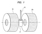
- FIG. 1 is a perspective view schematically showing main parts of an example of NMR equipment which is an objective of the invention.
- a uniform magnetic field of 14.1 tesla (T) is generated along the center line indicated by an alternate long and short dash line.
- a cryo-probe 31 is disposed in the direction orthogonal to the center line of the magnetic field.
- a probe coil of the cryo-probe 31 can be cooled down to 10K.
- a sample tube 32 having an inner diameter of about 10 mm in which a sample having a diameter of 3 to 10 mm and a length of 5 to 10 mm is disposed is inserted to the heat-insulated inside of the probe 31.
- a cooling system, a signal system, and electric circuits are not shown here.
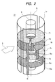
- FIGS. 2 and 3 are diagrams each illustrating an example of a primary idea of a configuration and a connection circuit used when a superconductor is applied to the solenoid coil of the cryo-probe 31.
- FIG. 2 is a perspective view schematically showing the configuration of the solenoid coil
- FIG. 3 is a circuit diagram of a case where the coil is used.
- reference numeral 3 denotes an arrow indicative of the direction of the uniform magnetic field generated by the superconducting magnets 30 1 and 30 2 .
- Each of 4 1 , 4 2 , 4 3 , and 4 4 denotes a donut-shaped coil part as a unit fabricated by a superconducting thin film formed on a donut plate-type substrate 2.
- the donut-shaped superconducting thin film has a slit extending in the radial direction by which the film is discontinued in the circumferential direction.
- the superconducting thin film coil parts 4 1 , 4 2 , 4 3 , and 4 4 are disposed in parallel with each other at predetermined intervals.
- 1 1 and 1 2 denote two divided parts of an outer cylinder for holding the superconducting thin film coil parts 4 1 , 4 2 , 4 3 , and 4 4 .
- the outer cylinder is divided into halves for convenience of assembling work.
- Reference numeral 9 denotes an inner cylinder for holding the superconducting thin film coil parts 4 1 , 4 2 , 4 3 , and 4 4 .
- the superconducting thin film coil parts are maintained at predetermined intervals and held so as to be parallel with each other by the inner cylinder 9 and the outer cylinder 1.
- the superconducting thin film coil parts 4 1 , 4 2 , 4 3 , and 4 4 4 as units constructing the coil are disposed so as to be parallel with the uniform magnetic field 3.
- Reference numerals 8 1 , 8 21 , 8 22 , 8 23 , and 8 24 denote normal metal leads.
- the lead 8 1 is connected to one end of the superconducting thin film coil part 4 1 and led to the lower end of the probe 31.
- the lead 8 21 connects one end of the superconducting thin film coil part 4 1 and one end of the superconducting thin film coil part 4 2 .
- the lead 8 22 connects one end of the superconducting thin film coil part 4 2 and one end of the superconducting thin film coil part 4 3 .
- the lead 8 23 connects one end of the superconducting thin film coil part 4 3 and one end of the superconducting thin film coil part 4 4 .
- the lead 8 24 is connected to the other end of the superconducting thin film coil part 4 4 and is led to the lower end of the probe 31. In such a manner, a solenoid coil having four turns is constructed between the leads 8 1 and 8 24 . To avoid occurrence of electric interference when the lead 8 1 passes the side faces of the other superconducting thin film coil parts 4 2 , 4 3 , and 4 4 , a slit is formed in the part where the lead 8 1 passes in the superconducting thin film of each of the superconducting thin film coil parts 4 2 , 4 3 , and 4 4 .
- the donut plate-type substrate 2 on which the superconducting thin film coil part 4 is formed is not shown.
- the superconducting thin film coil parts 4 may have the same configuration, to make the relations among the coil parts easily understood, the pattern of the superconducting thin film coil parts 4 1 and 4 3 and that of the superconducting thin film coil parts 4 2 , and 4 4 are made different from each other.
- the inner cylinder 1 and the outer cylinder 9 are made of, for example, sapphire and only the outlines of them are shown here.
- FIG. 3 is a circuit diagram of the case where the solenoid coil constructed as shown in FIG. 2 is used as a transmit/receive coil of 600 MHz so as to be provided for NMR spectroscopy by being cooled to 10K via the inner cylinder 1 and the outer cylinder 9 made of sapphire.
- a capacitor 6 of small capacitance of 0.17 pF to both ends of the leads 8 1 and 8 24 of the solenoid coil in parallel with a radio-frequency power source 7, the resultant can be used as a transmit/receive coil of 600 MHz. It is, however, extremely difficult to manufacture the capacitor 6 of small capacity of 0.17 pF or the like with high reproducibility and the operation becomes unstable. Thus, it is not realistic for the radio-frequency NMR equipment.
- the solenoid coil applies a magnetic field to a sample to be measured having a diameter of 3 to 10 mm and a length of 5 to 10 mm, which is put in the sample tube 32, and for receiving a free induction decay (FID) signal.
- the number of turns of the coil was set to 3 or larger, and a concrete target is to achieve the capacitance of 3 pF or larger which can be realized, of a capacitor as a component of a resonator of 600 MHz.
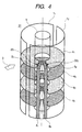
- FIG. 4 is a schematic figure of a probe coil for NMR equipment of Example 1.
- a donut plate-type coil part as a unit fabricated by a superconducting thin film formed on the donut plate-type substrate 2 (refer to FIG. 5B) and having a slit in the radial direction is basically employed.
- the donut plate-type substrate 2 is omitted and only outlines of the inner cylinder 9 and the outer cylinder 1 are shown.
- the patterns of the superconducting coil parts are made alternately different from each other so as to be distinguished from each other.
- Each of the halves 1 1 and 1 2 of the outer cylinder 1 has a shape obtained by dividing a sapphire pipe having an outside diameter of 20 mm and an inside diameter of 16.5 mm into halves.
- the inner cylinder 9 is a sapphire pipe having an outside diameter of 14 mm and an inside diameter of 11 mm.
- the donut plate-type substrate 2 is a donut plate-type flat substrate having an outside diameter of 18 mm, an inside diameter of 14 mm, and a thickness of 0.75 mm and is made of sapphire (Al 2 O 3 ) having a surface orientation of (0001). Four pieces of the donut plate-type substrates 2 are fixed at intervals of 3.3 mm.
- the superconducting thin film 4 is made of magnesium diboride (MgB 2 ).
- the magnesium diboride (MgB 2 ) superconducting thin film 4 was obtained by forming an amorphous MgB 2 film having a thickness of 250 nm on the surface of the donut plate-type substrate 2 made of sapphire by sputtering using a target in which B pellets are arranged on an Mg plate, heated at 400 °C at 2 ⁇ 10 -5 Torr for five minutes, and crystallized.
- the donut plate-type coil part made of the superconducting thin film 4 is disposed so as to be parallel with the uniform magnetic field 3 of the NMR equipment.
- connection between the superconducting thin film and the normal metal lead was not mentioned by referring to FIG. 2, in the probe coil 31 for NMR equipment of Example 1, the impedance of a coil part as a unit is reduced and stable connection between the superconducting thin film 4 of the coil part and the normal metal lead 8 is achieved by devising the connection part.
- Reference numerals 5 1 and 5 2 denote Au thin films and are formed in the position of the slit which is formed in the radial direction of the superconducting thin film 4 1 formed on the surface of the donut plate-type substrate 2.
- Reference numerals 22 1 and 22 2 denote overlap portions of the Au thin film 5 extended on the superconducting thin film 4 via an interlayer dielectric thin film 24.
- the Au thin film 5 and the overlap portion 22 are similarly formed on the other superconducting thin films 4, they are behind the normal metal leads 8 1 and 8 2 in FIG. 4 and are seen only partly.
- the coil parts as units formed by the superconducting thin films 4 are connected in parallel and are led to the lower end of the probe 31 by the normal metal leads 8 1 and 8 2 via the capacitor as will be described later.
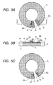
- FIG. 5A is a plane figure illustrating the relation between the coil part formed by the superconducting thin film 4 and the Au thin film 5 and FIG. 5B is a diagram taken along ling B-B' of FIG. 5A.
- the superconducting thin film 4 is formed on one of the surfaces of the donut plate-type substrate 2. A part of the superconducting thin film 4 is removed by etching, thereby forming a slit 21. After that, an aluminum nitride (AlN) film 23 is formed so as to cover the slit 21 including a part of both ends of the superconducting thin film 4. In a manner similar to the superconducting thin film 4, the aluminum nitride film 23 is formed by sputtering aluminum in nitrogen atmosphere by using a metal mask. After that, the Au thin film 5 is deposited and a pattern is formed so that the Au thin film 5 partially overlaps the superconducting thin film 4, thereby forming the overlap portions 22 1 and 22 2 .
- AlN aluminum nitride
- the slit 21 is formed at a pitch of 15°, and the Au thin film 5 and the overlap portions 22 1 and 22 2 are formed in the slit 21 close to the superconducting thin film 4.
- the outer circumferential portion of the donut plate-type substrate 2 of the Au thin film 5 is connected to the normal metal leads 8 1 and 8 2 .
- the normal metal leads 8 1 and 8 2 and the Au thin film 5 are in direct contact with each other but the superconducting thin film 4 and the normal metal leads 8 1 and 8 2 are not in direct contact with each other.
- FIG. 5B by sandwiching the aluminum nitride (AlN) film 24 between the Au thin film 5 and the superconducting thin film 4, capacitors 23 1 and 23 2 are formed in the overlap portions 22 1 and 22 2 , respectively.
- AlN aluminum nitride
- the capacitance of the capacitor 23 can be designed to 4 pF by making the interlayer dielectric thin film 24 of AlN, setting the thickness to 250 nm, and setting the size of the overlap portion 22 to 6 ⁇ m ⁇ 6 ⁇ m. Although the capacitance of the capacitor 23 was 4 pF in Example 1, it was found by computer simulation that by changing the size of the overlap portion 22, the capacitor 23 having capacitance in the range from 20 to 50 pF can be realized.
- FIG. 5C is a plane figure showing another form of the relation between the coil part formed by the superconducting thin film 4 and the Au thin film 5.
- a superconducting coil part is formed by slitting a part of the superconducting thin film 4, and the Au thin film 5 and the capacitor 23 as pieces in contact with the normal metal lead are formed in the slit 21.
- the effective length of the coil part formed by the superconducting thin film 4 can be increased.
- FIG. 6 is a circuit diagram of the case where the probe coil 31 for the NMR equipment illustrated in FIG. 5 is used as a transmit/receive coil of 600 MHz.
- the normal metal lead 8 and the coil part as a unit made by the superconducting thin film 4 are connected to each other via the capacitor 23.
- the superconducting thin film coil parts 4 1 , 4 2 , 4 3 , and 4 4 are connected to the normal metal leads 8 1 and 8 2 in parallel via the capacitors 23 11 and 23 12 in series, capacitors 23 21 and 23 22 in series, capacitors 23 31 and 23 32 in series, and capacitors 23 41 and 23 42 in series, respectively.
- the value of inductance evaluated between the normal metal leads 8 1 and 8 2 could be made low.
- a transmit/receive coil in which the capacitance of the capacitor 6 connected in parallel between the feeding points of the normal metal leads 8 1 and 8 2 is set to 40 pF was obtained.
- the transmit/receive coil of 600 MHz which functions stably could be obtained.
- the coil parts as units of the coil, formed by the superconducting thin films 4 on the donut plate-type substrates 2 are electrically connected to each other via the normal metal lead 8 by the Au thin film formed by evaporation on the inner surface of the outer cylinder 1.
- FIGS. 7 and 8 are diagrams illustrating fixation of the donut plate-type disc substrate 2 on which the superconducting thin film 4 is formed to the outer cylinder 1 and connection between the Au thin film 5 and the normal metal lead 8.
- grooves 13 1 , 13 2 , 13 3 , and 13 4 were provided at intervals corresponding to the intervals of the superconducting thin film coil parts 4 1 , 4 2 , 4 3 , and 4 4 as units of the coil in the inner surface of the divided part 1 2 of the outer cylinder 1.
- the depth of the groove 13 was set to 0.5 mm in correspondence with the outer diameter of the donut plate-type substrate 2 which was set to 18 mm in relation with the inner diameter of 16.5 mm of the outer cylinder 1. Since the thickness of the donut plate-type substrate 2 was set to 0.75 mm, the width of the groove 13 was set to 0.77 mm in correspondence with the thickness.
- the pitch of arranging the grooves 13 was set to 3.3 mm since the pitch of arranging the donut plate-type substrates 2 was set to 3.3 mm.
- An Au thin film was formed by evaporation on the inner surface of the half 1 2 of the outer cylinder 1 and the normal metal leads 8 1 and 8 2 were patterned.
- FIG. 8 is a cross section showing a part of the groove 13 in the normal metal lead 8 illustrated in FIG. 7.
- the normal metal lead 8 is formed by the Au thin film and, in the portion of the groove 13, recessed along the groove 13.
- the substrate 2 is inserted in the groove 13 so that the Au thin film 5 of the donut plate-type substrate 2 on which the superconducting thin film 4 and the Au thin film 5 are formed is positioned in the place where the normal metal lead 8 is formed in the groove 13.
- indium 14 is adhered by ultrasound as shown in FIG. 8.
- the inner cylinder 9 is inserted on the inside of the donut plate-type substrates 2. Further, the four donut plate-type disc substrates 2 are sandwiched by the other half 1 2 of the outer cylinder 1, and the halves 1 1 and 1 2 of the outer cylinder 1 are fixed in a cylindrical shape by a thermal-contraction tube.
- the fabricated 4-layer parallel coil was measured and tested.
- the sensitivity became 3.5 times as high as that in the case of using a copper coil.
- FIG. 9 is a diagram showing dependency on width of the sensitivity of the superconducting coil 4.
- the width of the superconducting coil 4 was 2 mm in Example 1, the width was changed from 0.3 mm to 4 mm. It is understood from the result that, when the width is increased, the conductor resistance and inductance decrease and the sensitivity improves. On the other hand, when the coil becomes larger, the outer diameter of the probe increases. Consequently, the distance from the sample increases and the sensitivity deteriorates. In addition, a contradictory effect occurs such that the uniformity of a static magnetic field B 0 deteriorates.
- the width of the superconducting thin film 4 is preferably in the range from 0.5 mm to 2 mm, more preferably, from 0.5 mm to 1 mm.
- Example 1 the grooves are formed on the inside of the supporting member for supporting the probe from the outside, and the donut plate-type substrates 2 are inserted and fixed in the grooves. In such a manner, the superconducting thin film 4 formed on the donut plate-type substrate 2 can be made parallel with the uniform magnetic field B 0 .
- This assembly manner can be also applied in the following other examples.
- a 4-layer parallel coil was formed in the same structure as that in Example 1 except that magnesium diboride (MgB 2 ) was changed to YBa 2 CU 3 O y (YBCO) as one of oxide superconductors.
- the donut plate-type substrate 2 was made of an La-Sr-Al-Ta oxide and the YBCO superconducting thin film 4 was formed by the pulsed laser deposition method. The same film thickness of 250 nm was used.
- the interlayer dielectric thin film 24 for forming the capacitor 23 between the superconducting thin film 4 and the normal metal lead 8 was formed by depositing cerium oxide (CeO 2 ) by using a metal mask by laser vapor deposition in a manner similar to the superconducting thin film 4.
- the Au thin film 5 was deposited in a manner similar to Example 1 and a pattern was formed so that the superconducting thin film 4 and the Au thin film 5 overlap partially.
- the slit 21 and the Au thin film 5 were formed at the pitch of 15 degrees, and the thickness of the Au thin film 5 was set to 200 nm.
- heat treatment was carried out at 400 °C for one hour in oxygen.
- the interlayer dielectric thin film 24 was made of CeO 2 and had a thickness of 300 nm, and the size of the overlap portion 22 was set to 6 ⁇ m ⁇ 6 ⁇ m, thereby enabling a capacitor having capacitance of 4 pF to be fabricated.
- the fabricated 4-layer parallel coil was measured and tested at 600 MHz. As a result, the sensitivity was improved by 3.5 times as high as that in the case of using a copper coil and the difference due to the superconductor material different from that of Example 1 was not found out.
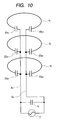
- FIG. 10 is a circuit diagram showing connection.
- the superconducting thin film 4 used in Example 3 is a YBCO film in a manner similar to Example 1 and an LaAlO 3 having a surface orientation of (001) was used for the donut plate-type substrate 2.
- the normal metal electrode constructing the capacitor 23 was formed by using an Ag thin film in place of the Au thin film.
- the thickness of the Ag thin film was 250 nm.
- the Ag thin film was vapor deposited and, after that, heat treatment at 400 °C for one hour was carried out in oxygen.
- the fabricated 3-layer parallel coil was measured and tested at 600 MHz. As a result, though the sensitivity decreases as compared with that in the case of Example 1, the sensitivity was three times as high as that in the case of using a copper coil.
- FIG. 11 is a schematic diagram of the coil
- FIGS. 12A to 12D are plane figures of the superconducting thin film coil parts 4 1 , 4 2 , 4 3 , and 4 4 forming the coil
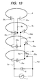
- FIG. 13 is a diagram showing connection of the superconducting thin film coil parts.
- the donut plate-type substrate 2 is omitted and only outlines of the inner cylinder 9 and the outer cylinder 1 are shown.
- the patterns of the superconducting coil parts are made alternately different from each other so as to be distinguished from each other.
- Example 4 In a manner similar to Example 1, the superconducting coil part 4 and the normal metal electrode formed by the Au thin film 5 are connected to each other via the capacitor 23, and the Au thin film 5 and the normal metal lead 8 are connected to each other.
- the same reference numerals are assigned to parts of the coil in FIG. 11 equivalent to those of FIG. 4 as a schematic diagram of the coil of Example 1.
- Example 4 to connect the superconducting thin film coil parts 4 1 , 4 2 , 4 3 , and 4 4 in series, as obvious from comparison between FIGS. 11 and 4, the positions of the normal metal electrodes formed the Ag thin films 5 are deviated sequentially by 7.5° corresponding to the width of one normal metal electrode formed by the Ag thin film 5.
- the start end of the superconducting thin film coil part 4 1 is led by the normal metal lead 8 1 in a manner similar to FIG. 4 but the other end of the coil part 4 1 is led by the metal lead 8 21 and connected to the start end of the coil part 4 2 .
- ends of the superconducting thin films are sequentially connected via the metal leads 8 22 and 8 23 and the other end of the last thin film coil part 4 4 is led by the metal lead 8 24 .
- the pattern structure of the overlap portion 22 as a component of the capacitor 23 shown in FIG. 5C was employed. In such a manner, the effective length of the superconducting coil 4 can be increased.
- FIGS. 12A to 12D are diagrams concretely showing the positional relations between the superconducting coil parts 4 1 , 4 2 , 4 3 , and 4 4 and the normal metal electrode formed by the Ag thin film 5.
- the diagrams also show notches 25 2 , 25 3 , and 25 4 in the superconducting coil parts 4 2 , 4 3 , and 4 4 provided for avoiding interference between the normal metal electrode formed by the Ag thin film 5 and the normal metal lead 8 1 .
- the normal metal electrode 5 2 formed by the Au thin film 5 of the superconducting coil part 4 1 and the normal metal electrode 5 12 formed by the Au thin film 5 of the superconducting coil part 4 2 are connected to each other via the normal metal lead 8 21 .
- the normal metal electrode 5 22 formed by the Au thin film 5 of the superconducting coil part 4 2 and the normal metal electrode 5 13 formed by the Au thin film 5 of the superconducting coil part 4 3 are connected to each other via the normal metal lead 8 22 .
- the normal metal electrode 5 23 formed by the Au thin film 5 of the superconducting thin film 4 3 and the normal metal electrode 5 14 formed by the Au thin film 5 of the superconducting thin film 4 4 are connected to each other via the normal metal lead 8 23 .
- the normal metal electrode 5 24 formed by the Au thin film 5 of the superconducting thin film 4 4 is led by the normal metal lead 8 24 .
- FIG. 13 is a connection diagram showing connection among the superconducting coil parts 4 1 , 4 2 , 4 3 , and 4 4 .
- the circuit configuration of the superconducting coil parts 4 1 , 4 2 , 4 3 , and 4 4 is similar to that of Example 1 shown in FIG. 6.
- Example 4 is different from Example 1 with respect to the point that the superconducting coil parts 4 1 , 4 2 , 4 3 , and 4 4 are arranged in series.
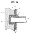
- Example 4 Fixation of the donut plate-type substrate 2 to the halves 1 1 and 1 2 of the outer cylinder 1 and connection between the superconducting coil part 4 and the normal metal lead 8 are similar to those of Example 1. However, different from Example 1, since connection among the superconducting coil parts 4 1 , 4 2 , 4 3 , and 4 4 is different from that of the normal metal leads 8 21 , 8 22 , and 8 23 , the normal metal lead 8 2 has to be patterned accordingly. In Example 4, as shown in FIG. 14, the normal metal lead 8 has a three-layer structure of an Au layer 15, an SiO 2 layer 16, and an Au layer 17.
- the Au layer 15 has a thickness of 200 nm
- the SiO 2 layer 16 has a thickness of 300 nm
- the Au layer 17 has a thickness of 200 nm.
- the Au layer 15 is grounded.
- the indium 14 was adhered by ultrasound to the Au layer 17 and the normal metal electrode 5.
- the manufactured four-layered serial superconducting coil was measured and tested at 600 MHz.
- the sensitivity improves by 2.7 times as high as that in the case of using a copper coil.
- the superconducting coil parts 4 1 , 4 2 , 4 3 , and 4 4 are connected via the capacitors 23, also in the case of using the coil at 600 MHz, the capacitance of the capacitor 6 connected in parallel with the feeding point increases to 2.7 pF. Thus, reproducibility improves.
- the thickness of Cu was set to 200 nm and that of Al was set to 100 nm.
- the coil was measured and tested at 600 MHz and it was found that the capacitance of the capacitor 6 connected in parallel with the feeding point increased to 3.6 pF at the same sensitivity as that in the case of parallel connection.
- Example 6 In the case where all of the superconducting coil parts 4 1 , 4 2 , 4 3 , and 4 4 are connected in series as in Example 1, even in the case of the invention, the value of inductance becomes large. Consequently, the capacitance of the capacitor 6 connected to the feeding point has to be reduced, so that it is disadvantageous for measurement at higher frequency.
- Example 6 two pairs of superconducting coil parts each connected in series were connected in parallel.
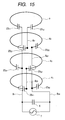
- FIG. 15 is a circuit diagram schematically showing Example 6. The superconducting coil parts 4 1 and 4 2 were connected in series, the superconducting coil parts 4 3 , and 4 4 were connected in series, and the pairs were connected in parallel. The same reference numerals as those in FIG. 13 showing the connection circuit of Example 4 were designated. The same pattern structure of the overlap portion 22 in the capacitor 23 as that of FIG. 5C in Example 4 was employed. With the configuration, the effective length of the superconducting coil 4 can be increased.
- FIG. 16 is a diagram illustrating the improved fixing method of Example 6.
- FIG. 8 illustrating the fixing method of Example 1, a section of a portion of a groove 18 in a part of the normal metal lead 8 is shown.
- the groove 18 as a tapered notch having a width of 0.75 mm, a depth of 0.5 mm, and an inclination angle of 10 to 15° was formed in the outer cylinder 1.
- the normal metal lead 8 employs a stacked structure of copper (Cu) and aluminum (Al) explained in Example 5.
- a Cu thin film 19 and an Al thin film 20 were formed with the same thickness as that in Example 5, and the pattern of the normal metal lead 8 for connecting the coil to the inner surface of the outer cylinder 1 was formed.
- the outer periphery of a width of 0.5 mm of the donut plate-type substrate 2 was tapered at the inclination angle of 10°, and the superconducting thin film 4 and the Au thin film 5 were formed on the processed substrate.
- Four donut plate-type substrates 2 were sandwiched by the two halves 1 1 and 1 2 of the outer cylinder 1 so as to be inserted in the notches 18 in the outer cylinder 1, and the outer cylinder 1 was fixed by a thermal contraction tube. Further, in a manner similar to Example 1, to secure electric contact between the normal metal led 8 and the Au thin film 5 and fixation of the donut plate-type substrate 2, the indium 14 was adhered by ultrasound.
- the taper formed on the inside of the outer cylinder 1 may not be necessarily formed on the Au thin film 5 side but may be formed on the side on which the substrate 2 is exposed. Alternately, tapers may be formed on both sides. In any of the cases, obviously, the periphery of the donut plate-type substrate 2 should be formed in a shape corresponding to the taper.
- Example 2 Test was made at 600 MHz in a manner similar to Example 1 and it was found that the capacitance of the capacitor 6 connected in parallel with the feeding point increased to 10.4 pF at the same sensitivity as that in the case where four superconducting coil parts 4 of Example 1 are connected in parallel.
- the sensitivity of the probe coil and the necessary capacitance of the capacitor 6 in the case where the normal metal lead 8 and the superconducting coil were connected in series (direct connection) as shown in FIG. 2 and the case where the normal metal lead 8 and the superconducting coil were connected so as to interpose the capacitor 23 between them were evaluated.
- the capacitance of the capacitor 23 constructed between the normal metal lead 8 and the superconducting coil was set to 4 pF and the measurement frequency was set as 600 MHz.
- Table 1 shows results of the evaluation.
- Table 1 shows results of the evaluation.
- the necessary capacitance of the capacitor 6 for power feeding is shown in parenthesis and, for comparison, the case where a normal metal coil is used as the coil is also shown.
- Sensitivity in various coil shapes and necessary capacitance of capacitor connecting method coil 4 coil parts in parallel two parallel pairs each constructed 4 coil parts connected direct connection normal conductor 104.76 (6.7 pF) 133.09 (1.35 pF) 148.37 (0.17 pF) super-conductor 366.77 (6.7 pF) 399.75 (1.35 pF) 428.74 (0.17 pF) capacitive connection() normal conductor 112.54 (39 pF) 127.01 (10.3 pF) 137.93 (2.7 pF) super-conductor 379.19 (40 pF) 370.95 (10.4 pF) 374.56 (2.7 pF)
- the coil shape to be employed differs according to the frequency used, it was clarified that, by connecting the superconducting coil to the normal metal lead via the capacitor to thereby form a solenoid coil, sensitivity which is higher by three times or more can be obtained. Since the capacitance of the feeding capacitor 6 can be made large, reproducibility in manufacture can be improved largely.
- a probe coil having a structure characterized by using MgB2 for the superconducting thin film and connection to the normal metal lead via the same capacitor as that in Example 1 was fabricated.
- polytetrafluoroethylene was used for a donut plate-type substrate.
- An MgB 2 thin film was formed by sputtering using a target in which B pellets are arranged on an Mg plate like in Example 1. After formation of the thin film, heat treatment was carried at 2 ⁇ 10 -5 Torr at 400 °C for two minutes by lamp heating to crystallize the film.
- An AlN interlayer dielectric thin film was formed on the MgB 2 superconducting thin film and, after that, the Au thin film 5 serving as the overlap portion 22 and the connection piece constructing the capacitor 23 was formed.
- the pattern of the superconducting thin film and the pattern of the Au thin film for the capacitor and the contact are the same as those in Example 1. In this case as well, performances similar to those of Example 1 were obtained.
- the capacitor 23 is requested to have withstand voltage.
- a single capacitor 23 in which the interlayer dielectric thin film 24 is made of CeO 2 shown in Example 1 is disadvantageous from the viewpoint of withstand voltage.
- an example of the capacitor 23 formed by connecting a plurality of capacitors in series is proposed.
- FIG. 17A is a plane figure of the slit portion in the superconducting coil part 4 1 and the overlap portion 22 of the Au thin film 5 of Example 8, and FIG. 17B is a cross section taken along line B-B' of FIG. 17A.
- a YBCO superconducting thin film constructing the superconducting coil having a thickness of 250 nm was formed and lower electrodes 36 1 , 36 2 , 36 3 and 36 4 were patterned simultaneously with patterning of the superconducting coil part 4 1 .
- an SrTiO 3 interlayer dielectric thin film 38 was formed.
- the thickness of the SrTiO 3 interlayer dielectric thin film 38 was 200 nm.
- upper electrodes 37 1 , 37 2 , 37 3 , and 37 4 patterned so as to bridge the slit in the superconducting thin film 4 1 and the patterns of the lower electrodes 36 1 , 36 2 , 36 3 and 36 4 were formed.
- the Au thin film 5 was formed and, simultaneously, the overlap portion 22 was also formed.
- FIGS. 17A and 17B There are overlap portions between the slits in the superconducting coil part 4 1 and the lower electrodes 36 1 , 36 2 , 36 3 and 36 4 and the upper electrodes 37 1 , 37 2 , 37 3 , and 37 4 .
- the overlap portions therefore function as capacitors.
- FIGS. 17A and 17B nine capacitors are connected in series between the normal metal lead 8 and the Au thin film 5 of the connection portion of the superconducting coil part 4 1 .
- FIG. 17C is a diagram showing connection of the superconducting coil part 4 1 to the normal metal leads 8 1 and 8 2 via the capacitors 23 1 and 23 2 connected in series.
- the capacitor 23 By forming the capacitor 23 by connecting plural capacitors in series, the voltage applied to each of the capacitors becomes lower, so that the break down voltage in the case where the coil is used as a transmit coil can be increased.
- SrTiO 3 having very high relative dielectric constant is used for an interlayer dielectric thin film in order to increase the capacitance of each of the capacitors and to maintain the capacitance as a whole also when the capacitors are connected in series.
- Another example of the material having high relative dielectric constant is BaTiO 3 .
- the superconducting thin films in parallel with the magnetic field and connecting the superconducting thin films to the normal metal lead, without disturbing the magnetic field, implementation of superconductor into the probe coil can be achieved. Further, by disposing a capacitor at a connection point between the superconducting thin film and the normal metal lead, the size of the capacitor connected to the feeding point can be set to a size which can be easily controlled. As a result, an FID signal in NMR spectroscopy can be detected with high sensitivity.
Landscapes
- Physics & Mathematics (AREA)
- Condensed Matter Physics & Semiconductors (AREA)
- General Physics & Mathematics (AREA)
- Electromagnetism (AREA)
- Superconductor Devices And Manufacturing Methods Thereof (AREA)
- Magnetic Resonance Imaging Apparatus (AREA)
Applications Claiming Priority (2)
| Application Number | Priority Date | Filing Date | Title |
|---|---|---|---|
| JP2003165099A JP4090389B2 (ja) | 2003-06-10 | 2003-06-10 | 核磁気共鳴装置 |
| JP2003165099 | 2003-06-10 |
Publications (2)
| Publication Number | Publication Date |
|---|---|
| EP1486793A2 true EP1486793A2 (fr) | 2004-12-15 |
| EP1486793A3 EP1486793A3 (fr) | 2005-09-07 |
Family
ID=33296810
Family Applications (1)
| Application Number | Title | Priority Date | Filing Date |
|---|---|---|---|
| EP04012588A Withdrawn EP1486793A3 (fr) | 2003-06-10 | 2004-05-27 | Bobine supraconductrice de sonde r.f. pour la résonance magnétique |
Country Status (3)
| Country | Link |
|---|---|
| US (1) | US6958608B2 (fr) |
| EP (1) | EP1486793A3 (fr) |
| JP (1) | JP4090389B2 (fr) |
Cited By (8)
| Publication number | Priority date | Publication date | Assignee | Title |
|---|---|---|---|---|
| EP1643261A1 (fr) * | 2004-08-11 | 2006-04-05 | Hitachi, Ltd. | Appareil à résonance magnétique nucléaire |
| EP1666908A1 (fr) * | 2004-12-02 | 2006-06-07 | Hitachi, Ltd. | Bobine solénoidale supraconductrice de sonde à résonance magnétique nucléaire |
| WO2007118719A1 (fr) * | 2006-04-13 | 2007-10-25 | Siemens Aktiengesellschaft | Résonateur pour des applications de résonance magnétique |
| EP2145197A4 (fr) * | 2007-05-04 | 2011-07-27 | California Inst Of Techn | Géométries pour bobines de détection de supraconductivité destinées à des systèmes basés sur un squid |
| CN102820116A (zh) * | 2012-05-04 | 2012-12-12 | 清华大学 | 一种高温超导薄膜磁体 |
| CN110412065A (zh) * | 2019-06-19 | 2019-11-05 | 广西电网有限责任公司电力科学研究院 | 一种用于复合绝缘子老化检测的核磁共振传感器 |
| WO2020217069A1 (fr) * | 2019-04-26 | 2020-10-29 | Oxford University Innovation Limited | Bobine radiofréquence |
| US11360140B1 (en) | 2020-12-18 | 2022-06-14 | Microsoft Technology Licensing, Llc | RF functional probe |
Families Citing this family (46)
| Publication number | Priority date | Publication date | Assignee | Title |
|---|---|---|---|---|
| CA2309002A1 (fr) * | 2000-05-23 | 2001-11-23 | Jonathan Martin Shekter | Reduction du grain de films utilises en photographie numerique |
| JP2003329756A (ja) * | 2002-05-08 | 2003-11-19 | Hitachi Ltd | 超高感度核磁気共鳴イメージング装置 |
| JP3993127B2 (ja) * | 2003-04-24 | 2007-10-17 | 株式会社日立製作所 | Nmr装置用超電導プローブコイル |
| US7521932B2 (en) * | 2003-05-06 | 2009-04-21 | The Penn State Research Foundation | Method and system for adjusting the fundamental symmetric mode of coupled high temperature superconductor coils |
| US7295085B2 (en) * | 2003-08-21 | 2007-11-13 | E.I. Du Pont De Nemours And Company | Process for making high temperature superconductor devices each having a line oriented in a spiral fashion |
| WO2005045447A2 (fr) * | 2003-11-05 | 2005-05-19 | New York University | Dispositif de gradient de champ et son procede d'utilisation |
| US20070245374A1 (en) * | 2003-11-24 | 2007-10-18 | Inventec Corporation | Video program subtitle tex recording method and system |
| US7332910B2 (en) * | 2003-11-24 | 2008-02-19 | E.I. Du Pont De Nemours And Company | Frequency detection system comprising circuitry for adjusting the resonance frequency of a high temperature superconductor self-resonant coil |
| US7301344B2 (en) | 2003-11-24 | 2007-11-27 | E.I. Du Pont De Nemours & Co. | Q-damping circuit including a high temperature superconductor coil for damping a high temperature superconductor self-resonant coil in a nuclear quadrupole resonance detection system |
| WO2005059582A1 (fr) * | 2003-12-15 | 2005-06-30 | E.I. Dupont De Nemours And Company | Utilisation de plusieurs detecteurs dans un systeme de detection a resonance quadripole nucleaire visant l'augmentation de la vitesse de mesure |
| WO2005078468A2 (fr) * | 2004-01-20 | 2005-08-25 | The University Of Houston System | Boucle supraconductrice, bobines d'irm en selle de cheval et en cage a oiseaux |
| WO2005078469A1 (fr) * | 2004-02-04 | 2005-08-25 | E.I. Dupont De Nemours And Company | Utilisation d'au moins deux capteurs pour la detection de signaux de resonance quadrupolaire nucleaire d'un compose cible |
| EP1711840A2 (fr) * | 2004-02-04 | 2006-10-18 | E.I.Du pont de nemours and company | L'utilisation de deux capteurs ou plus dans un système de détection de résonance nucléaire à quadrupôle afin d'améliorer un rapport signal sur bruit |
| DE102004020298A1 (de) * | 2004-04-26 | 2005-11-10 | Covion Organic Semiconductors Gmbh | Elektrolumineszierende Polymere und deren Verwendung |
| WO2006073452A2 (fr) * | 2004-04-30 | 2006-07-13 | E.I. Dupont De Nemours And Company | Procedes et appareil pour balayer une bande de frequences en utilisant un reseau de capteurs supraconducteurs haute temperature |
| US7265549B2 (en) | 2004-04-30 | 2007-09-04 | E. I. Du Pont De Nemours And Company | Scanning a band of frequencies using an array of high temperature superconductor sensors tuned to the same frequency |
| US7279897B2 (en) * | 2004-04-30 | 2007-10-09 | E. I. Du Pont De Nemours And Company | Scanning a band of frequencies using an array of high temperature superconductor sensors tuned to different frequencies |
| US7782059B2 (en) * | 2004-11-23 | 2010-08-24 | M2M Imaging Corp. | Bandwidth expansion in magnetic resonance |
| EP1825288A2 (fr) | 2004-12-03 | 2007-08-29 | E.I. Dupont De Nemours And Company | Procede pour la reduction du couplage entre des bobines d'excitation et de reception d'un systeme de detection par resonance quadripolaire nucleaire |
| JP4593255B2 (ja) * | 2004-12-08 | 2010-12-08 | 株式会社日立製作所 | Nmr装置およびnmr計測用プローブ |
| WO2006065929A1 (fr) | 2004-12-13 | 2006-06-22 | E. I. Du Pont De Nemours And Company | Alarme aux masques metalliques d'un systeme de detection de la contrebande rqn/rayons x |
| US7456630B2 (en) * | 2005-09-22 | 2008-11-25 | U Chicago Argonne Llc | NMR characterization of thin films |
| US7859374B2 (en) * | 2005-10-03 | 2010-12-28 | Massachusetts Institute Of Technology | Annular magnet system for magnetic resonance spectroscopy |
| WO2007049426A1 (fr) * | 2005-10-25 | 2007-05-03 | Hitachi, Ltd. | Sonde et appareil a resonance magnetique nucleaire |
| JP5006542B2 (ja) * | 2005-12-26 | 2012-08-22 | 株式会社日立製作所 | Nmr装置およびnmr計測用プローブ |
| JP4787033B2 (ja) * | 2006-02-15 | 2011-10-05 | 株式会社日立製作所 | 核磁気共鳴信号用ソレノイドコイル及び核磁気共鳴信号取得装置 |
| JP4971685B2 (ja) | 2006-05-25 | 2012-07-11 | 株式会社日立製作所 | 核磁気共鳴プローブコイル |
| JP5232379B2 (ja) | 2006-11-09 | 2013-07-10 | 株式会社日立製作所 | Nmr計測用プローブ、およびそれを用いたnmr装置 |
| JP4861149B2 (ja) * | 2006-12-08 | 2012-01-25 | 株式会社日立製作所 | 核磁気共鳴装置 |
| JP4394716B2 (ja) * | 2007-11-14 | 2010-01-06 | 株式会社日立製作所 | Nmr計測用プローブ |
| DE102007054592B4 (de) * | 2007-11-15 | 2014-04-30 | Siemens Aktiengesellschaft | Steckverbindungsvorrichtung, ausgebildet zur Verbindung zweier Funktionselemente zur Signal- und Leistungsübertragung |
| JP2011518409A (ja) * | 2008-03-30 | 2011-06-23 | ヒルズ, インコーポレイテッド | 超伝導ワイヤおよびケーブルならびにその製造方法 |
| JP5222324B2 (ja) * | 2010-07-14 | 2013-06-26 | 株式会社日立製作所 | 超電導コイル、超電導マグネットおよびその運転方法 |
| KR101414779B1 (ko) * | 2010-10-20 | 2014-07-03 | 한국전자통신연구원 | 무선 전력 전송 장치 |
| CN104081478B (zh) * | 2011-09-26 | 2017-10-10 | 欧文·罗斯 | 螺线管圆环 |
| US9519037B2 (en) * | 2011-11-10 | 2016-12-13 | Mayo Foundation For Medical Education And Research | Spatially coincident MRI receiver coils and method for manufacturing |
| DE102012201370B4 (de) * | 2012-01-31 | 2016-02-11 | Siemens Aktiengesellschaft | Halterung für Double-Loop-Coil (Doppel-Schleifen-Spule) für z.B. MCP-Aufnahmen |
| DE102012213594B4 (de) * | 2012-08-01 | 2016-07-28 | Siemens Healthcare Gmbh | MR- Oberflächenspule mit integrierter automatischer Patientenfixierung |
| DE102013217555B3 (de) * | 2013-09-03 | 2014-12-04 | Siemens Aktiengesellschaft | Kombinierte Shim- und HF-Spulenelemente |
| HK1252007A1 (zh) | 2015-05-12 | 2019-05-10 | Hyperfine, Inc. | 射频线圈方法和装置 |
| CN110579502B (zh) * | 2019-09-29 | 2023-03-28 | 西安石油大学 | 一种用于核磁共振两相流测量的传感器 |
| GB2590633A (en) * | 2019-12-20 | 2021-07-07 | Tokamak Energy Ltd | HTS linked partial insulation for HTS field coils |
| CN114764078B (zh) * | 2021-01-14 | 2025-08-15 | 中国科学院宁波材料技术与工程研究所 | 一种高温核磁共振探头和高温核磁共振装置 |
| DE102022206766B3 (de) | 2022-07-01 | 2023-11-30 | Bruker Switzerland Ag | NMR-Probenkopf mit einer Sende-Empfangsspule umfassend einen Hinwicklungsabschnitt und einen Rückwicklungsabschnitt |
| CN115831524B (zh) * | 2022-11-04 | 2026-04-03 | 华中科技大学 | 一种超大电流密度超导磁体及其无线励磁装置 |
| CN117148241B (zh) * | 2023-10-30 | 2024-02-06 | 天津天达图治科技有限公司 | 一种智能超材料结构 |
Family Cites Families (65)
| Publication number | Priority date | Publication date | Assignee | Title |
|---|---|---|---|---|
| US2697893A (en) * | 1951-07-21 | 1954-12-28 | Fred W Hoch | Combination planishing plate and method of making the same |
| GB1100423A (en) * | 1964-02-24 | 1968-01-24 | American Can Co | Method and device for treating a smooth plastic sheet surface to reduce its coefficient of friction with respect to a smooth body surface |
| US3389036A (en) * | 1964-06-16 | 1968-06-18 | Interchem Corp | Method of making polyethylene laminates |
| US3504075A (en) * | 1967-10-26 | 1970-03-31 | Eastman Kodak Co | Method of manufacturing high-gloss polymeric films |
| US3758192A (en) * | 1970-08-20 | 1973-09-11 | Minnesota Mining & Mfg | Reflex-reflective structures including fabric and transfer foils |
| US4021179A (en) * | 1973-06-01 | 1977-05-03 | Agfa-Gevaert N.V. | Apparatus for the edges of thermoplastic webs |
| IT1075393B (it) * | 1977-04-13 | 1985-04-22 | Sir Soc Italiana Resine Spa | Film accoppiati flessibili per l'imballaggio di prodotti alimentari |
| JPS5474862A (en) * | 1977-11-28 | 1979-06-15 | Fuji Photo Film Co Ltd | Thickening device |
| US4525134A (en) * | 1979-07-20 | 1985-06-25 | American Can Company | Apparatus for making a multi-layer injection blow molded container |
| US4447485A (en) * | 1981-08-04 | 1984-05-08 | Mitsubishi Plastics Industries Limited | Adhesive tape and process for its production |
| US4376147A (en) * | 1981-08-31 | 1983-03-08 | Clopay Corporation | Plastic film having a matte finish |
| JPS58128853A (ja) * | 1982-01-27 | 1983-08-01 | 住友化学工業株式会社 | 農業用フイルム |
| US4532189A (en) * | 1982-02-19 | 1985-07-30 | W. R. Grace & Co., Cryovac Div. | Linear polyethylene shrink films |
| US4643943A (en) * | 1984-05-30 | 1987-02-17 | W. R. Grace & Co., Cryovac Div. | Multi-layer polyolefin shrink film |
| US4546029A (en) * | 1984-06-18 | 1985-10-08 | Clopay Corporation | Random embossed matte plastic film |
| US5372669A (en) * | 1985-02-05 | 1994-12-13 | Avery Dennison Corporation | Composite facestocks and liners |
| US4946532A (en) * | 1985-02-05 | 1990-08-07 | Avery International Corporation | Composite facestocks and liners |
| DE3650593T2 (de) * | 1985-02-05 | 1997-09-11 | Avery International Corp | Verbundfutter |
| GB2181670B (en) * | 1985-10-18 | 1989-09-13 | Ashimori Ind Co Ltd | Tubular lining material for pipelines |
| JPS62268621A (ja) * | 1986-05-16 | 1987-11-21 | Okura Ind Co Ltd | 積層未延伸原反フイルムの製造方法 |
| US4896943A (en) * | 1987-05-13 | 1990-01-30 | Minnesota Mining And Manufacturing Company | Encapsulated-lens retroreflective sheeting having improved cover film |
| CA1331480C (fr) * | 1987-05-18 | 1994-08-16 | Arthur Davidson | Conducteurs a courants intenses et aimants a champs intenses utilisant des supraconducteurs anisotropes |
| JP3148821B2 (ja) * | 1987-05-21 | 2001-03-26 | グンゼ株式会社 | 食品包装材及びその製造法 |
| US4895760A (en) * | 1987-10-09 | 1990-01-23 | Tredegar Industries, Inc. | Film coating for rigid, smooth surfaces |
| US5100709A (en) * | 1987-10-09 | 1992-03-31 | Tredegar Industries, Inc. | Multilayer film coating for rigid, smooth surfaces |
| US5127974A (en) * | 1989-05-15 | 1992-07-07 | Kansai Paint Co., Ltd. | Method of protecting coating film |
| US5229358A (en) * | 1989-06-15 | 1993-07-20 | Microelectronics And Computer Technology Corporation | Method and apparatus for fabricating superconducting wire |
| US5064802A (en) * | 1989-09-14 | 1991-11-12 | The Dow Chemical Company | Metal complex compounds |
| US5158836A (en) * | 1991-02-21 | 1992-10-27 | W. R. Grace & Co.-Conn. | Oriented film of high clarity and gloss |
| US5219666A (en) * | 1990-03-23 | 1993-06-15 | W.R. Grace & Co.-Conn. | Oriented film of high clarity and gloss |
| DE4013111C2 (de) | 1990-04-25 | 1994-05-26 | Spectrospin Ag | HF-Empfangsspulenanordnung für NMR-Spektrometer |
| US5272236A (en) * | 1991-10-15 | 1993-12-21 | The Dow Chemical Company | Elastic substantially linear olefin polymers |
| JP2545006B2 (ja) * | 1990-07-03 | 1996-10-16 | ザ ダウ ケミカル カンパニー | 付加重合触媒 |
| CA2048296C (fr) * | 1990-08-13 | 2002-09-24 | Henry G. Schirmer | Melanges de copolymere de propylene et d'ethylene, et pellicules faites a partir de ceux-ci |
| WO1992008429A1 (fr) * | 1990-11-13 | 1992-05-29 | Mobil Oil Corporation | Materiau en feuille de polypropylene presentant une meilleure resistance a la coupe |
| US5112423A (en) * | 1991-01-02 | 1992-05-12 | Liebe Jr Robert J | Method of making and applying alignment-maintaining plastic lettering material |
| US5702790A (en) * | 1991-01-02 | 1997-12-30 | Liebe, Jr.; Robert James | Water-added evaporation process for making thin plastic lettering webs |
| US5441785A (en) * | 1991-01-02 | 1995-08-15 | Liebe, Jr.; Robert J. | Composite alignment-maintaining plastic lettering material |
| JPH04256292A (ja) * | 1991-02-08 | 1992-09-10 | Sharp Corp | 固体撮像装置 |
| TW200424B (fr) * | 1991-09-09 | 1993-02-21 | Avery Dennison Corp | |
| US5344680A (en) * | 1991-10-09 | 1994-09-06 | Gerber Scientific Products, Inc. | Sign making web with tack killing overcoat removable by washing and related method |
| US5525695A (en) * | 1991-10-15 | 1996-06-11 | The Dow Chemical Company | Elastic linear interpolymers |
| US5496295A (en) * | 1991-12-18 | 1996-03-05 | Minnesota Mining And Manufacturing Company | Multilayered barrier structures |
| DE69224287T2 (de) * | 1992-01-06 | 1998-08-27 | The Dow Chemical Co., Midland, Mich. | Katalysatorzusammensetzung |
| EP0561552B1 (fr) * | 1992-03-17 | 1997-10-15 | Hitachi, Ltd. | Générateur de champ magnétique, interrupteur de courant persistant pour un tel générateur de champ magnétique et méthode de contrÔle pour un tel générateur de champ magnétique |
| US5585723A (en) * | 1995-03-23 | 1996-12-17 | Conductus, Inc. | Inductively coupled superconducting coil assembly |
| US5296277A (en) * | 1992-06-26 | 1994-03-22 | Minnesota Mining And Manufacturing Company | Positionable and repositionable adhesive articles |
| JP3477557B2 (ja) * | 1992-09-17 | 2003-12-10 | 株式会社フジシール | フィルムチューブおよびセンターシール方法 |
| US5268228A (en) * | 1992-09-21 | 1993-12-07 | Norwood Industries, Inc. | Grooved pressure-sensitive adhesive tape |
| US5460878A (en) * | 1992-10-26 | 1995-10-24 | Applied Extrusion Technologies, Inc. | Heat sealable shrink laminate |
| US5468532A (en) * | 1992-12-10 | 1995-11-21 | Minnesota Mining And Manufacturing Company | Multilayer graphic article with color layer |
| US5346963A (en) * | 1993-04-28 | 1994-09-13 | The Dow Chemical Company | Graft-modified, substantially linear ethylene polymers and methods for their use |
| US5470993A (en) * | 1993-06-24 | 1995-11-28 | The Dow Chemical Company | Titanium(II) or zirconium(II) complexes and addition polymerization catalysts therefrom |
| US5585193A (en) * | 1993-07-16 | 1996-12-17 | Avery Dennison Corporation | Machine-direction oriented label films and die-cut labels prepared therefrom |
| US5451283A (en) * | 1993-07-16 | 1995-09-19 | Avery Dennison Corporation | Method of making a uniaxially oriented label film with compatibilizer |
| US5486632A (en) * | 1994-06-28 | 1996-01-23 | The Dow Chemical Company | Group 4 metal diene complexes and addition polymerization catalysts therefrom |
| JPH10508706A (ja) * | 1994-11-07 | 1998-08-25 | ミネソタ マイニング アンド マニュファクチャリグ カンパニー | 標示製品及びその製造方法 |
| US5693405A (en) * | 1995-01-13 | 1997-12-02 | Tredegar Industries, Inc. | Masking film having embossed areas and unembossed areas |
| WO1997010924A1 (fr) * | 1995-09-18 | 1997-03-27 | Minnesota Mining And Manufacturing Company | Matiere de blocage de lentilles thermoplastiques |
| DE19622082C1 (de) * | 1996-05-31 | 1997-11-20 | Brueckner Maschbau | Verfahren zur Herstellung einer füllstoffhaltigen bedruckbaren Polymerfolie |
| WO1998025163A1 (fr) * | 1996-12-02 | 1998-06-11 | The Trustees Of Columbia University In The City Of New York | Sonde supraconductrice a resonance multiple |
| US5716086A (en) * | 1997-01-17 | 1998-02-10 | Bifulco; Phil | Pizza paddle apparatus |
| DE19733574C2 (de) | 1997-08-02 | 2000-04-06 | Bruker Ag | Supraleitender Hybrid-Resonator für den Empfang für NMR-Signalen |
| JP2003255032A (ja) | 2002-02-28 | 2003-09-10 | Hitachi Ltd | 核磁気共鳴装置用プローブ |
| JP4122833B2 (ja) | 2002-05-07 | 2008-07-23 | 株式会社日立製作所 | 二ホウ化マグネシウムを用いたnmr装置用プローブ |
-
2003
- 2003-06-10 JP JP2003165099A patent/JP4090389B2/ja not_active Expired - Fee Related
-
2004
- 2004-05-25 US US10/852,254 patent/US6958608B2/en not_active Expired - Fee Related
- 2004-05-27 EP EP04012588A patent/EP1486793A3/fr not_active Withdrawn
Cited By (14)
| Publication number | Priority date | Publication date | Assignee | Title |
|---|---|---|---|---|
| EP1643261A1 (fr) * | 2004-08-11 | 2006-04-05 | Hitachi, Ltd. | Appareil à résonance magnétique nucléaire |
| US7173424B2 (en) | 2004-08-11 | 2007-02-06 | Hitachi, Ltd. | Nuclear magnetic resonance apparatus |
| EP1666908A1 (fr) * | 2004-12-02 | 2006-06-07 | Hitachi, Ltd. | Bobine solénoidale supraconductrice de sonde à résonance magnétique nucléaire |
| US7164269B2 (en) | 2004-12-02 | 2007-01-16 | Hitachi, Ltd. | Nuclear magnetic resonance probe coil |
| WO2007118719A1 (fr) * | 2006-04-13 | 2007-10-25 | Siemens Aktiengesellschaft | Résonateur pour des applications de résonance magnétique |
| US7579836B2 (en) | 2006-04-13 | 2009-08-25 | Siemens Aktiengesellschaft | Multi-layer resonator for magnetic resonance applications with the resonator structure itself allowing equal magnitude current during active operation |
| EP2145197A4 (fr) * | 2007-05-04 | 2011-07-27 | California Inst Of Techn | Géométries pour bobines de détection de supraconductivité destinées à des systèmes basés sur un squid |
| CN102820116A (zh) * | 2012-05-04 | 2012-12-12 | 清华大学 | 一种高温超导薄膜磁体 |
| CN102820116B (zh) * | 2012-05-04 | 2014-11-26 | 清华大学 | 一种高温超导薄膜磁体 |
| WO2020217069A1 (fr) * | 2019-04-26 | 2020-10-29 | Oxford University Innovation Limited | Bobine radiofréquence |
| CN110412065A (zh) * | 2019-06-19 | 2019-11-05 | 广西电网有限责任公司电力科学研究院 | 一种用于复合绝缘子老化检测的核磁共振传感器 |
| CN110412065B (zh) * | 2019-06-19 | 2021-06-22 | 广西电网有限责任公司电力科学研究院 | 一种用于复合绝缘子老化检测的核磁共振传感器 |
| US11360140B1 (en) | 2020-12-18 | 2022-06-14 | Microsoft Technology Licensing, Llc | RF functional probe |
| WO2022132331A1 (fr) * | 2020-12-18 | 2022-06-23 | Microsoft Technology Licensing, Llc | Sonde fonctionnelle rf |
Also Published As
| Publication number | Publication date |
|---|---|
| US20040251902A1 (en) | 2004-12-16 |
| US6958608B2 (en) | 2005-10-25 |
| EP1486793A3 (fr) | 2005-09-07 |
| JP4090389B2 (ja) | 2008-05-28 |
| JP2005003435A (ja) | 2005-01-06 |
Similar Documents
| Publication | Publication Date | Title |
|---|---|---|
| US6958608B2 (en) | Nuclear magnetic resonance equipment | |
| US7619414B2 (en) | NMR probe and NMR spectrometer | |
| EP0654147B1 (fr) | Bobine exploratrice supraconductrice a resonance magnetique | |
| US6377047B1 (en) | Superconducting birdcage coils | |
| EP1061378B1 (fr) | Procédé de fabrication d'une bobine d'une sonde à résonance magnétique nucléaire | |
| EP1669772B1 (fr) | Spectromètre RMN et bobine supraconductrice de sonde à résonance magnétique | |
| US5585723A (en) | Inductively coupled superconducting coil assembly | |
| US5594342A (en) | Nuclear magnetic resonance probe coil with enhanced current-carrying capability | |
| US20080039332A1 (en) | Method and System for the Production of Superconducting Inductive Components Comprising Thin Layers, and Devices Containing Such Components | |
| US6121776A (en) | Superconducting hybrid-resonator for receiving NMR-signals | |
| JP2002328156A (ja) | 局部磁場発生素子及びコンデンサ素子を備えるnmr平面コイル | |
| US7173424B2 (en) | Nuclear magnetic resonance apparatus | |
| KR20060100442A (ko) | 고온 초전도체 자기 공진 코일의 공진 주파수 조절용회로를 포함하는 주파수 검출 시스템 | |
| US7248046B2 (en) | Decoupling high temperature superconductor sensor arrays in nuclear quadrupole resonance detection systems | |
| US5466480A (en) | Method for making an NMR coil | |
| US7436182B1 (en) | Cryogenic NMR probe capacitors with dielectric heat sinks | |
| JP2000507351A (ja) | rf―SQUID磁力計を超伝導タンク共振回路に結合するための配置 | |
| JPH0460556B2 (fr) | ||
| MXPA01002713A (es) | Dispositivos de filtro y resonador de superconduccion, y metodos para fabricar los mismos.. | |
| JPH0431069B2 (fr) |
Legal Events
| Date | Code | Title | Description |
|---|---|---|---|
| PUAI | Public reference made under article 153(3) epc to a published international application that has entered the european phase |
Free format text: ORIGINAL CODE: 0009012 |
|
| AK | Designated contracting states |
Kind code of ref document: A2 Designated state(s): AT BE BG CH CY CZ DE DK EE ES FI FR GB GR HU IE IT LI LU MC NL PL PT RO SE SI SK TR |
|
| AX | Request for extension of the european patent |
Extension state: AL HR LT LV MK |
|
| PUAL | Search report despatched |
Free format text: ORIGINAL CODE: 0009013 |
|
| AK | Designated contracting states |
Kind code of ref document: A3 Designated state(s): AT BE BG CH CY CZ DE DK EE ES FI FR GB GR HU IE IT LI LU MC NL PL PT RO SE SI SK TR |
|
| AX | Request for extension of the european patent |
Extension state: AL HR LT LV MK |
|
| 17P | Request for examination filed |
Effective date: 20060227 |
|
| AKX | Designation fees paid |
Designated state(s): CH DE GB LI |
|
| 17Q | First examination report despatched |
Effective date: 20091202 |
|
| STAA | Information on the status of an ep patent application or granted ep patent |
Free format text: STATUS: THE APPLICATION IS DEEMED TO BE WITHDRAWN |
|
| 18D | Application deemed to be withdrawn |
Effective date: 20100413 |