EP1486829A2 - Trägerplattensystem, Belichtungsanlage und Verfahren zur Herstellung einer Vorrichtung - Google Patents
Trägerplattensystem, Belichtungsanlage und Verfahren zur Herstellung einer Vorrichtung Download PDFInfo
- Publication number
- EP1486829A2 EP1486829A2 EP04253447A EP04253447A EP1486829A2 EP 1486829 A2 EP1486829 A2 EP 1486829A2 EP 04253447 A EP04253447 A EP 04253447A EP 04253447 A EP04253447 A EP 04253447A EP 1486829 A2 EP1486829 A2 EP 1486829A2
- Authority
- EP
- European Patent Office
- Prior art keywords
- guide
- movable
- stage system
- directions
- parallel
- Prior art date
- Legal status (The legal status is an assumption and is not a legal conclusion. Google has not performed a legal analysis and makes no representation as to the accuracy of the status listed.)
- Withdrawn
Links
Images


Classifications
-
- G—PHYSICS
- G03—PHOTOGRAPHY; CINEMATOGRAPHY; ANALOGOUS TECHNIQUES USING WAVES OTHER THAN OPTICAL WAVES; ELECTROGRAPHY; HOLOGRAPHY
- G03F—PHOTOMECHANICAL PRODUCTION OF TEXTURED OR PATTERNED SURFACES, e.g. FOR PRINTING, FOR PROCESSING OF SEMICONDUCTOR DEVICES; MATERIALS THEREFOR; ORIGINALS THEREFOR; APPARATUS SPECIALLY ADAPTED THEREFOR
- G03F7/00—Photomechanical, e.g. photolithographic, production of textured or patterned surfaces, e.g. printing surfaces; Materials therefor, e.g. comprising photoresists; Apparatus specially adapted therefor
- G03F7/70—Microphotolithographic exposure; Apparatus therefor
- G03F7/708—Construction of apparatus, e.g. environment aspects, hygiene aspects or materials
- G03F7/70808—Construction details, e.g. housing, load-lock, seals or windows for passing light in or out of apparatus
-
- G—PHYSICS
- G03—PHOTOGRAPHY; CINEMATOGRAPHY; ANALOGOUS TECHNIQUES USING WAVES OTHER THAN OPTICAL WAVES; ELECTROGRAPHY; HOLOGRAPHY
- G03F—PHOTOMECHANICAL PRODUCTION OF TEXTURED OR PATTERNED SURFACES, e.g. FOR PRINTING, FOR PROCESSING OF SEMICONDUCTOR DEVICES; MATERIALS THEREFOR; ORIGINALS THEREFOR; APPARATUS SPECIALLY ADAPTED THEREFOR
- G03F7/00—Photomechanical, e.g. photolithographic, production of textured or patterned surfaces, e.g. printing surfaces; Materials therefor, e.g. comprising photoresists; Apparatus specially adapted therefor
- G03F7/70—Microphotolithographic exposure; Apparatus therefor
- G03F7/70691—Handling of masks or workpieces
- G03F7/70716—Stages
-
- G—PHYSICS
- G03—PHOTOGRAPHY; CINEMATOGRAPHY; ANALOGOUS TECHNIQUES USING WAVES OTHER THAN OPTICAL WAVES; ELECTROGRAPHY; HOLOGRAPHY
- G03F—PHOTOMECHANICAL PRODUCTION OF TEXTURED OR PATTERNED SURFACES, e.g. FOR PRINTING, FOR PROCESSING OF SEMICONDUCTOR DEVICES; MATERIALS THEREFOR; ORIGINALS THEREFOR; APPARATUS SPECIALLY ADAPTED THEREFOR
- G03F7/00—Photomechanical, e.g. photolithographic, production of textured or patterned surfaces, e.g. printing surfaces; Materials therefor, e.g. comprising photoresists; Apparatus specially adapted therefor
- G03F7/70—Microphotolithographic exposure; Apparatus therefor
- G03F7/70691—Handling of masks or workpieces
- G03F7/70758—Drive means, e.g. actuators, motors for long- or short-stroke modules or fine or coarse driving
-
- G—PHYSICS
- G03—PHOTOGRAPHY; CINEMATOGRAPHY; ANALOGOUS TECHNIQUES USING WAVES OTHER THAN OPTICAL WAVES; ELECTROGRAPHY; HOLOGRAPHY
- G03F—PHOTOMECHANICAL PRODUCTION OF TEXTURED OR PATTERNED SURFACES, e.g. FOR PRINTING, FOR PROCESSING OF SEMICONDUCTOR DEVICES; MATERIALS THEREFOR; ORIGINALS THEREFOR; APPARATUS SPECIALLY ADAPTED THEREFOR
- G03F7/00—Photomechanical, e.g. photolithographic, production of textured or patterned surfaces, e.g. printing surfaces; Materials therefor, e.g. comprising photoresists; Apparatus specially adapted therefor
- G03F7/70—Microphotolithographic exposure; Apparatus therefor
- G03F7/708—Construction of apparatus, e.g. environment aspects, hygiene aspects or materials
- G03F7/70808—Construction details, e.g. housing, load-lock, seals or windows for passing light in or out of apparatus
- G03F7/70816—Bearings
-
- H—ELECTRICITY
- H01—ELECTRIC ELEMENTS
- H01J—ELECTRIC DISCHARGE TUBES OR DISCHARGE LAMPS
- H01J37/00—Discharge tubes with provision for introducing objects or material to be exposed to the discharge, e.g. for the purpose of examination or processing thereof
- H01J37/02—Details
- H01J37/20—Means for supporting or positioning the object or the material; Means for adjusting diaphragms or lenses associated with the support
-
- H—ELECTRICITY
- H02—GENERATION; CONVERSION OR DISTRIBUTION OF ELECTRIC POWER
- H02K—DYNAMO-ELECTRIC MACHINES
- H02K1/00—Details of the magnetic circuit
- H02K1/06—Details of the magnetic circuit characterised by the shape, form or construction
- H02K1/22—Rotating parts of the magnetic circuit
- H02K1/27—Rotor cores with permanent magnets
- H02K1/2706—Inner rotors
- H02K1/272—Inner rotors the magnetisation axis of the magnets being perpendicular to the rotor axis
- H02K1/274—Inner rotors the magnetisation axis of the magnets being perpendicular to the rotor axis the rotor consisting of two or more circumferentially positioned magnets
- H02K1/2753—Inner rotors the magnetisation axis of the magnets being perpendicular to the rotor axis the rotor consisting of two or more circumferentially positioned magnets the rotor consisting of magnets or groups of magnets arranged with alternating polarity
- H02K1/278—Surface mounted magnets; Inset magnets
-
- H—ELECTRICITY
- H02—GENERATION; CONVERSION OR DISTRIBUTION OF ELECTRIC POWER
- H02K—DYNAMO-ELECTRIC MACHINES
- H02K41/00—Propulsion systems in which a rigid body is moved along a path due to dynamo-electric interaction between the body and a magnetic field travelling along the path
- H02K41/02—Linear motors; Sectional motors
- H02K41/03—Synchronous motors; Motors moving step by step; Reluctance motors
- H02K41/031—Synchronous motors; Motors moving step by step; Reluctance motors of the permanent magnet type
-
- H—ELECTRICITY
- H01—ELECTRIC ELEMENTS
- H01J—ELECTRIC DISCHARGE TUBES OR DISCHARGE LAMPS
- H01J2237/00—Discharge tubes exposing object to beam, e.g. for analysis treatment, etching, imaging
- H01J2237/20—Positioning, supporting, modifying or maintaining the physical state of objects being observed or treated
- H01J2237/202—Movement
- H01J2237/20292—Means for position and/or orientation registration
-
- H—ELECTRICITY
- H01—ELECTRIC ELEMENTS
- H01J—ELECTRIC DISCHARGE TUBES OR DISCHARGE LAMPS
- H01J2237/00—Discharge tubes exposing object to beam, e.g. for analysis treatment, etching, imaging
- H01J2237/30—Electron or ion beam tubes for processing objects
- H01J2237/317—Processing objects on a microscale
- H01J2237/3175—Lithography
-
- H—ELECTRICITY
- H02—GENERATION; CONVERSION OR DISTRIBUTION OF ELECTRIC POWER
- H02K—DYNAMO-ELECTRIC MACHINES
- H02K16/00—Machines with more than one rotor or stator
-
- H—ELECTRICITY
- H02—GENERATION; CONVERSION OR DISTRIBUTION OF ELECTRIC POWER
- H02K—DYNAMO-ELECTRIC MACHINES
- H02K2201/00—Specific aspects not provided for in the other groups of this subclass relating to the magnetic circuits
- H02K2201/18—Machines moving with multiple degrees of freedom
Definitions
- This invention relates to a stage system to be used in various measuring instruments or in a projection exposure apparatus for a semiconductor lithography process, for moving and positioning a substrate such as a wafer at a high speed and with a high precision.
- the stage system of the present invention is best suited for a stage system particularly to be used in an electron beam exposure apparatus, in which an electron beam is used to perform pattern drawing for direct patterning of a wafer or reticle exposure, or in an EUV (extreme ultraviolet) exposure apparatus using EUV light as exposure light in which the stage system is used in a vacuum ambience.
- EUV extreme ultraviolet
- the manufacture of devices such as semiconductor device is based on lithography technology in which various patterns formed on a mask are transferred to a wafer in a reduced scale, by use of light. Extremely high precision is required in relation to the mask pattern to be used in such lithography technology, and an electron beam exposure apparatus is used to make such a mask. Further, an electron beam exposure apparatus is used also in a case where a pattern is to be directly formed on a wafer without using a mask.
- the apparatus comprises an electron gun unit for producing an electron beam, an electron optical system for directing the produced electron beam to a sample, a stage system for scanningly moving the whole surface of the sample with respect to the electron beam, and an objective deflector for positioning the electron beam upon the sample very precisely.
- the region that can be positioned by use of an objective deflector has only a small size of about a few millimeters, to suppress the aberration of the electron optical system as much as possible.
- the size of the sample for a silicon wafer it is about 200 - 300 mm diameter, and for a glass substrate to be used as a mask, it is bout 150 mm square.
- the electron beam exposure apparatuses include a stage system by which the whole surface of the sample can be scanned with the electron beam.
- the positioning response of the electron beam is extraordinarily high, generally they use a system in which the attitude of the stage or a positional deviation thereof is measured and the measured value is fed back to the positioning of the electron beam through the deflector, rather than attempting to improve the mechanical control characteristic of the stage.
- the stage is disposed in a vacuum chamber and, furthermore, there is restriction that a change in magnetic field that may influence upon the positioning precision of the electron beam must be avoided, generally the stage is disposed by use of limited elements of contact type, such as rolling guides or ball screw actuators.
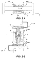
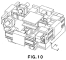
- Japanese Laid-Open Patent Application No. 2002-252166 shows a countermeasure therefor, and Figure 10 illustrates it, that is, a stage having two freedoms in planar directions, using vacuum air guides and linear motors.
- Figure 10 illustrates it, that is, a stage having two freedoms in planar directions, using vacuum air guides and linear motors.
- very smooth acceleration can be accomplished and, yet, with respect to the positioning direction, external disturbance from the guide is very small.
- the stage comprises an X slider, a Y slider and an X-Y slider, wherein the X slider and the Y slider are confined with respect to rotation about Z axis, by means of radial bearings.
- Figure 11 shows an example of a stage to be used in an atmosphere, corresponding to a stage disclosed in Japanese Laid-Open Patent Application No. 2002-8971.
- the stage comprises an X slider (X guide bar 28), a Y slider (Y guide bar 29), and an X-Y slider, but the X slider and the Y slider are not confined with respect to rotation about the Z axis.
- the election beam exposure apparatus there is a known example disclosed in Japanese Laid-Open Patent Application No. H09-330867.
- a plurality of electron beam are projected upon the surface of a sample along design coordinates and the electron beams are deflected along the design coordinates to thereby scan the sample surface.
- the electron beams are individually turned on and off to thereby draw the pattern.
- a desired pattern can be drawn by use of plural electron beams, and thus the throughput can be improved.
- Figure 12 illustrates a general structure of a multiple electron-beam type exposure apparatus.
- 501a, 501b, and 501c are electron guns by which a plurality of electron beams can be individually turned on and off.
- Denoted at 100 is a reduction electron optical system for reducing and projecting the electron beams from the electron guns 501a, 501b and 501c, onto a wafer 305.
- Denoted at 306 is a deflector for scanning the plural electron beams projected to the wafer 305.
- Figure 13 illustrates the action as a wafer is scanned with plural electron beams, in the exposure apparatus of Figure 12.
- White small circles depict beam reference positions BS1, BS2 and BS3 whereat the electron beams are incident as they are not deflected by the deflector 306.
- These beam reference positions BS1 - BS3 are placed along a design orthogonal coordinate system (Xs, Ys).
- the electron beams are scanned (scanningly deflected) also along a design orthogonal coordinate system (Xs, Ys) while taking the beam reference positions as a reference, to scan associated exposure fields EF1, EF2 and EF3, respectively.
- the stage which carries the wafer 350 thereon is scanningly moved mainly in Y direction as denoted at 200 in Figure 13, to perform sequential exposures of zones of the wafer.
- an embodiment of the present invention seeks to provide a high-precision stage system that can meet enlargement of the stroke.
- a stage system comprising: a first fixed guide having a first guide surface being parallel to or approximately parallel to a first direction and a second direction being orthogonal to or approximately orthogonal to the first direction; a first movable guide to be guided by said first fixed guide and having three freedoms of straight motions in the first and second directions and a motion in a rotational direction about a third direction being orthogonal to or approximately orthogonal to the first and second directions, said first movable guide having a first guide extending in the second direction; a second fixed guide having a second guide surface being parallel to or approximately parallel to the first and second directions; a second movable guide to be guided by said second fixed guide and having three freedoms of straight motions in the first and second directions and a motion in a rotational direction about the third direction, said second movable guide having a second guide extending in the first direction; and a central movable member to be guided in the first and second directions by means of said first and second
- a stage system comprising: a first fixed guide having a first guide surface being parallel to or approximately parallel to a first direction and a second direction being orthogonal to or approximately orthogonal to the first direction; a first movable guide to be guided by said first fixed guide and having a first guide extending in the second direction; a second fixed guide having a second guide surface being parallel to or approximately parallel to the first and second directions; a second movable guide to be guided by said second fixed guide and having a second guide extending in the first direction; a third fixed guide having a third guide surface being parallel to or approximately parallel to said first and second guide surfaces; and a central movable member to be guided in the first and second directions by means of said first and second guides, and also to be guided by said third fixed guide in a third direction being orthogonal to or approximately orthogonal to the first and second directions, wherein said central movable member is attracted to said third fixed guide by means of a permanent magnet unit having a magnetic
- An embodiment of the present invention seeks to provide a high-precision stage system that can meet enlargement of the stroke. Further, since the fixed guide (guide surface) is divided into plural guides, even if magnetic preload is used, magnets can be magnetically shielded effectively. Thus, the stage system can be well incorporated into an electron beam exposure apparatus.
- the present invention may take the following preferred forms.
- a stage system in one preferred from of the present invention comprises: a first fixed guide (1a, 1c: reference numerals are those used in the embodiments to be described later) having a plane (first guide surface) being parallel to or approximately parallel to a first direction (X direction) and a second direction (Y direction) being orthogonal to or approximately orthogonal to the first direction; a first movable guide (3) to be guided by the first fixed guide and having three freedoms including a motion in a rotational direction about a third direction being orthogonal to or approximately orthogonal to the first and second directions (the first movable guide having a guide 3f extending in the Y direction); a second fixed guide (1b, 1d) having a plane (second guide surface) being parallel to or approximately parallel to the first and second directions; a second movable guide (2) to be guided by the second fixed guide and having three freedoms in the first, second and third directions (the second movable guide having a guide 2f extending in the X direction); and a central movable
- the stage system may further comprise (i) a first actuator group (34m) for driving the first movable guide (3) in three-freedom directions (the first actuator group including a first X actuator for driving the first movable guide in the X direction with a relatively long stroke, and a first Y actuator for driving the first movable guide in the second direction with a relatively short stroke), and (ii) a second actuator group (24m) for driving the second movable guide (2) at least in two-freedom directions of X and Y (the second actuator group including a second Y actuator for driving the second movable guide in the Y direction with a relatively long stroke, and a second X actuator for driving the second movable guide in the X direction with a relatively short stroke).
- a first actuator group for driving the first movable guide (3) in three-freedom directions
- the first actuator group including a first X actuator for driving the first movable guide in the X direction with a relatively long stroke, and a first Y actuator for driving the first
- the stage system may further comprise a third fixed guide (1) having a plane extending in X and Y directions.
- the central movable member (4) may be guided by the third fixed guide.
- the upper surfaces of the first, second and third fixed guides, functioning as a guide surface, may be parallel to or approximately parallel to each other. These guides may comprise a static pressure bearing.
- the actuators may comprise a non-contact linear motor.
- the first X actuator may use a Y-direction magnetic flux component of a permanent magnet 134mag group (X movable element), while the first Y actuator may use an X-direction magnetic flux component of the permanent magnet group.
- the second Y actuator may use an X-direction magnetic flux component of a permanent magnet group (Y movable element), while the second X actuator may use a Y-direction magnetic flux component of the permanent magnet group.
- the state system may preferably further comprise a third fixed guide (1) having a plane in X and Y directions, and the central movable member (4) may be guided by the third fixed guide.
- a first magnet (39) may apply a preload to the first movable guide (3) with respect to the first fixed guide (1a, 1c), and a second magnet (29) may apply a preload to the second movable guide (2) with respect to the second fixed guide (1b, 1d).
- a third magnet (49) may apply a preload to the central movable member (4) with respect to the third fixed guide (1).
- the first, second and third magnets may have magnetic shields (39sh, 29sh, 49sh), respectively.
- each magnetic shield and the first, second and third magnets is Re
- the magnetic resistance of a magnetic path defined interactively between the first, second and third magnets is Rr
- Re ⁇ Rr the magnetic resistance of a magnetic path defined interactively between the first, second and third magnets
- the actuators may comprise non-contact linear motors, having a magnetic shield.
- the first Y actuator or the second X actuator may comprise an electromagnet.
- a stage system in a second preferred form of the present invention comprises: a first fixed guide (1a, 1c) having a plane (first guide surface) being parallel to or approximately parallel to a first direction (X direction) and a second direction (Y direction) being orthogonal to or approximately orthogonal to the first direction; a first movable guide (3) to be guided by said first fixed guide (the first movable guide having a Y guide 3f extending in the Y direction; a second fixed guide (1b, 1d) having a plane (second guide surface) being parallel to or approximately parallel to the first and second directions; a second movable guide (2) to be guided by said second fixed guide (the second movable guide having an X guide 2f extending in the X direction; a third fixed guide (1) having a third guide surface being parallel to or approximately parallel to said first and second guide surfaces; and a central movable member (4) to be guided in the X and Y directions by means of the Y guide (3f) and the X guide (2f), and also to be guided
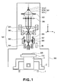
- FIG 1 is a schematic view of a main portion of an electron beam exposure apparatus according to an embodiment of the present invention.
- Denoted in Figure 1 at 300 is a vacuum sample chamber, and denoted at 301 is an electron gun having a cathode 301a, a grid 301b and an anode 301c. Electrons emitted from the cathode 301a produces a crossover image between the grid 301b and the anode 301c (hereinafter, the crossover image will be referred to as a light source).
- Electrons emitted from this light source are formed into an approximately parallel electron beam by means of a condenser lens 302 having a front focal point position placed at the light source position.
- the approximately parallel electron beam is then incident on an element electron optical system array 303.
- the element electron optical system array 303 includes a plurality of element electron optical systems each comprising a blanking electrode, aperture and an electron lens. These element electron optical systems are arrayed along a direction perpendicular to the optical axis of a reduction electron optical system 100 which is parallel to the Z axis. Details of the element electron optical system array 303 will be described later.
- the element electron optical system array 303 functions to produce a plurality of intermediate images of the light source, and these intermediate images are projected in a reduced scale by the reduction electron optical system 100, whereby light source images are formed upon a wafer 305.
- the components of the element electron optical system array 303 are set so that the spacing of the light source images formed on the wafer 305 has a size corresponding to a multiple, by an integral number, of the size of the light source.
- the element electron optical system 303 functions to assure that the positions of the light source images with respect to the optical axis direction are different in accordance with the field curvature of the reduction electron optical system 100.
- the element electron optical system functions to correct aberration to be produced as the intermediate images are projected on the wafer 305 by the reduction electron optical system 100.
- the reduction electron optical system 100 includes two-stage type symmetric magnetic tablets, comprising a first projection lens (341, 343) and a second projection lens (342, 344). Where the focal length of the first projection lens (341, 343) is f1 while the focal length of the second projection lens (342, 344) is f2, the distance between these two lenses is equal to f1+f2.
- the object point on the optical axis is at the focal point position of the first projection lens (341, 343), and the image point thereof is focused on the focal point of the second projection lens (342, 344).
- This image is reduced at -f2/f1.
- the magnetic fields of these two lenses are determined so that they act on in mutually opposite directions, theoretically, except five aberrations of spherical aberration, isotropic astigmatism, isotropic coma aberration, field curvature aberration, and longitudinal chromatic aberration, the remaining Seidel's aberration and chromatic aberration concerning rotation and magnification can be cancelled.
- Denoted at 306 is a deflector for deflecting plural electron beams from the element electron optical system array 303 so as to shift plural light source images upon the wafer 305 in X and Y directions by the same displacement amount. While not shown in the drawing, the deflector 306 comprises a main deflector to be used when the deflection width is wide, and a sub-deflector to be used when the deflection width is narrow.
- the main deflector is an electromagnetic type deflector
- the sub-deflector is an electrostatic type deflector.
- Denoted at 307 is a dynamic focus coil for correcting a deviation of the focus position of the light source image, based on deflection aberration to be produced when the deflector 306 is operated.
- Denoted at 308 is a dynamic coil which serves, like the dynamic focus coil 307, to correct astigmatism of deflection aberration to be produced by the deflection.
- Denoted at 99 is an alignment scope having an off-axis arrangement, for detecting a mark already formed on the wafer.
- Denoted at 310 is a top stage for carrying a wafer 305 thereon.
- the top stage 310 should have a stroke corresponding to the wafer diameter, just underneath the alignment scope 99.
- the X-Y slider 4 comprises an X-Y slider-(y) 41 and an X-Y slider-(x) 42. At the bottom of the X-Y slider-(y) 41, there is a vacuum proof bearing 43 disposed opposed to the top face 1f of a stage base 1. Also, inside the side wall of the X-Y slider-(y) 41, there is a similar vacuum proof bearing 44 disposed to sandwich a Y guide 3f.
- the Y guide 3f is formed at opposite side walls of an X beam 32 (providing X slider 3), in the lengthwise direction.
- the X guide 2f is formed at the opposite side walls of a Y beam (providing Y slider 2), in the lengthwise direction.
- the X slider 3 having the Y guide 3f and the Y slider 2 having the X guide 2f are formed in a grid-like shape as shown in Figure 3.
- the X slider 3 is moved in the X direction by which it can be moved smoothly along the X guide 2f and the stage base top face 1f.
- the Y slider 2 is moved in the Y direction by which it can be moved smoothly along the Y guide 3f and the stage base top face 1f.
- the Y slider 2 has a Y beam 22 including the X guide 2f, as well as a Y foot 21 and a Y foot 21' disposed on the opposite side with respect to the X direction. At the bottom of the Y foot 21 (21'), there is a vacuum proof bearing 23 disposed opposed to the top face a beam base 1b (1d).
- the top face of the beam base 1b (1d) is parallel to or approximately parallel to the stage base top face 1f.
- the Y slider 2 can move smoothly in the Y direction by a required stroke, within the range of the top face of the beam base 1b (1d), and also it can move smoothly in the X direction and a rotational direction about the Z axis (hereinafter, "Z-axis rotational direction").
- Z-axis rotational direction a rotational direction about the Z axis
- the Y slider 2 can move with a long stroke in the Y direction and with a short stroke in the X direction.
- adding the Z-axis rotational direction it can move with three freedoms.
- linear motor movable elements 24m disposed at the opposite sides in respect to the X direction, for driving the Y slider 2 in the Y direction.
- Each linear motor movable element 24m contains a permanent magnet therein, and a magnetic shield cover is mounted thereon to prevent leakage of magnetic field into the stage space.
- a linear motor for moving the Y slider 2 in the X direction is also housed in the movable element 24m. Details will be described later, with reference to Figure 4.
- the Y foot 21 is provided with a reflection mirror 26 for measuring the position in Y direction and a reflection mirror 26x for measuring the position in X direction, while the Y foot 21' is provided with a reflection mirror 26' for measuring the position in Y direction.
- the position (x, y, ⁇ z) of the Y slider 2 in the directions of X, Y and Z-axis rotation can be measured.
- the X slider 3 includes an X beam 32 having the Y guide 3f, and an X foot 31 and an X foot 31' disposed in opposite sides with respect to the Y direction. At the bottom of the X foot 31 (31'), there is a vacuum proof bearing 33 disposed opposed to the top face of a beam base 1a (1c).
- the top face of the beam base 1a (1c) is parallel to or approximately parallel to the stage base top face 1f.
- the X slider can move smoothly in the X direction by a required stroke, within the range of the top face of the beam base 1a (1c), and also it can move smoothly in the Y direction and the Z-axis rotational direction.
- the X slider 3 can move with a long stroke in the X direction and with a short stroke in the Y direction.
- adding the Z-axis rotational direction it can move with three freedoms.
- Each linear motor movable element 34m contains a permanent magnet therein, and a magnetic shield cover is mounted thereon to prevent leakage of magnetic field into the stage space.
- a linear motor for moving the X slider in the Y direction is also housed in the movable element 34m.
- the X foot 31 is provided with a reflection mirror 36 for measuring the position in X direction
- the X foot 31' is provided with a reflection mirror 36y for measuring the position in Y direction and a reflection mirror 36' for measuring the position in X direction.
- interferometer systems 136, 136' and 136y the position (x, y, ⁇ z) of the X slider 3 in the directions of X, Y and Z-axis rotation can be measured.
- Figure 3 is a diagram of a control system for the X and Y sliders.
- the values of the interferometer systems 136, 136' and 136y corresponding to the X slider 3 are converted by an X slider computing unit 130 into the X-direction position x, Y-direction position y and Z-axis rotational direction ⁇ z of the X slider 3, and they are applied as a feedback signal to an X slider controller 131.
- the X slider controller 131 calculates a driver designated value (Xfx, Xfx', Xfy) and, by applying an electric current to a coil array provided in an associated X stator 34s, driving forces Xfx and Xfx' in the X and Z-axis rotational directions as well as a driving force Xfy in the Y direction are produced.
- the values of the interferometer systems 126, 126' and 126x corresponding to the Y slider 2 are converted by a Y slider computing unit 120 into the X-direction position x and Y-direction position y of the Y slider 2, and they are applied as a feedback signal to a Y slider controller 121.
- the Y slider controller 121 calculates a driver designated value (Yfy, Yfx) and, by applying an electric current to a coil array provided in an associated Y stator 24s, driving forces Yfy in the Y direction as well as a driving force Yfx in the X direction are produced.
- the Z-axis rotation of the X slider 3 is controllably confined, while the Z-axis rotation of the Y slider 2 follows the rotation of the X slider 3.
- the X-direction position of the X-Y slider 4 can be regarded as being substantially equivalent to the X-direction position of the X slider 3
- the Y-direction position of the X-Y slider can be regarded as being substantially equivalent to the Y-direction position of the Y slider 2.
- the Z-axis rotation thereof can be regarded as being substantially equivalent to the Z-axis rotation of the X slider 3. Measurement for these rough-motion sliders can be performed in various combinations and, as an example, the X-Y slider 4 can be measured directly by use of an interferometer.
- a control may be added by using velocity information in rotational direction.
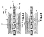
- the linear motor 34 has a movable element 34m and a stator 34s.
- the movable element 34m comprises a movable magnet 134mag and a magnetic shield 134sh.
- the stator 34 comprises coil arrays 134a, 134b, 134c, 134d and 134e which are disposed along the stroke direction. Each coil has a two-layer structure. There is a jacket 134j for covering the coil arrays, to prevent the coil arrays from being bared inside the vacuum sample chamber.
- the movable magnet 134mag includes X-direction magnetized magnets which are alternately sandwiched between Y-direction magnetized magnets, to provide a magnetic flux distribution near a sine wave in the coil space.
- Figure 4A illustrates a state in which a driving force acts on in the X direction.
- a Y-direction largest magnetic flux By is being produced at the coil b.
- a force is applied to the movable element 34m in the X direction.
- Figure 4B illustrates a state in which a driving force acts on in the Y direction.
- An X-direction largest magnetic flux Bx is being produced at the coil c, in opposite directions at the positions of the coils 134b_u and 134b_d.
- a force is applied to the movable element 34m in the Y direction.
- this force in the Y direction may be weak as compared with the force in the X direction, there does not occur a particular problem since the force in the Y direction is not used for acceleration of the X slider.
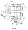
- Figure 5 illustrates an electromagnet arrangement as a second embodiment, for applying a driving force in Y direction for the X slider and a driving force in X direction for the Y slider.
- the X foot 31 and X foot 31' of the X slider 3 are provided with a linear motor movable element 34m" for applying an X-direction driving force and, additionally, the X foot 31' is provided with an electromagnet unit 34m' for applying a Y-direction driving force.
- the electromagnet unit 34m' includes an E-shaped core 234EM, a coil 234co and a magnetic shield 234sh, at the movable side, which are fixed to the X foot 31' by a non-magnetic material 235.
- the X slider 3 can be driven in Y direction by selectively applying and controlling a voltage to opposed coils.
- the Y foot 21 and the Y foot 21' of the Y slider 2 are provided with a linear motor movable element 24m" for applying a Y-direction driving force and, additionally, the Y foot 31' is provided with an electromagnet unit 24m' for applying an X-direction driving force.
- the electromagnet unit 24m' includes an E-shaped core 224EM, a coil 224co and a magnetic shield 224sh, at the movable side, which are fixed to the Y foot 21' by a non-magnetic material 235. Also, there is a magnetic material bar (I-shaped core) 224I at the fixed side, which is fixed to the beam base 1d by an I-shaped core mounting member 236 made of a non-magnetic material.
- the Y slider 2 can be driven in X direction by selectively applying and controlling a voltage to opposed coils.
- Figure 6A illustrates the whole structure as viewed from the bottom, for explaining the base arrangement for supporting the sliders.
- Figure 6B illustrates a single bottom pad.
- a vacuum proof bearing 43 disposed opposed to the top surface 1f of the stage base 1.
- a vacuum proof bearing 23 disposed opposed to the top surface of the beam base 1b (1d).
- a vacuum proof bearing 33 disposed opposed to the top surface of the beam base 1a (1c).
- each pad comprises a static-pressure bearing portion 51 in which a fluid is discharged through a porous material, a labyrinth portion 52 for preventing leakage of the discharged fluid into the ambience, and an exhaust bore 53.
- the labyrinth portion includes a plurality of lands 52L and grooves 52g, for providing a fluid resistance without contact.
- a preload is applied to the static-pressure bearing.
- a preload is applied on the basis of an attraction force of a permanent magnet.
- the preload application may be made by simple float type preload such as vacuum preload (in a case where the ambience is atmosphere or reduced pressure ambience) or magnet preload, or a confinement type load in which a preload is applied while a static-pressure bearing is disposed opposed.
- the simple float type preload based on magnet preload is used.
- denoted at 29 is a permanent magnet fixed to the Y foot
- denoted at 39 is a permanent magnet fixed to the X foot
- Denoted at 49 is a permanent magnet fixed to the X-Y slider-(y) 41 ( Figure 2).
- These magnets are covered by magnetic shields 29sh, 39sh and 49sh, for preventing leakage of their magnetic field. Since the confinement type preload is not used, only the bearing surface and the guide surface are the precision required surface.
- a structure as a confinement type preload is used as shown in Figure 2, that is, a vacuum proof bearing 45 is provided at the opposite sides of the inside wall of the X-Y slider-(x) 42 to sandwich the opposed X guide 2f therebetween.
- a vacuum proof bearing 45 is provided at the opposite sides of the inside wall of the X-Y slider-(x) 42 to sandwich the opposed X guide 2f therebetween.
- the parallelism of the opposite sides of the bearing 45 at the X-Y slider side as well as the parallelism of the opposite faces of the X guide 2f should be controlled. However, the rigidity will be improved in this case.
- the preload magnet 49 of the X-Y slider is disposed opposed to the stage base 1, and the preload magnet 29 of the Y slider is disposed opposed to the beam base 1b (1d).
- the preload magnet 39 of the X slider is disposed opposed to the beam base 1a (1c).
- the bases 1, 1a, 1b, 1c and 1d of them are disposed with a certain mutual magnetic resistance.
- Figure 6C shows a case wherein the bases are not magnetically isolated
- Figure 6D shows a case where the bases are isolated. If they are not isolated, in addition to magnetic circuits L1 produced by the respective magnets, a magnetic circuit L2 is produced between plural magnets and this leaks outwardly beyond the shields 29sh, 39sh and 49sh. On the other hand, if magnetic isolation is provided (that is, the magnetic resistance is enlarged sufficiently high), the magnetic flux leakage between plural magnets can be reduced as much as possible.
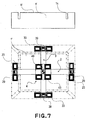
- Figure 7 illustrates the base arrangement according to a second embodiment, as viewed from the bottom.
- the base 1' to which the respective permanent magnets are disposed opposed is formed integrally.
- the precision setting at the guide surface 1f of the base 1' is easy.
- Figure 8A shows the base arrangement according to a third embodiment, as viewed from the bottom.
- Figure 8B illustrates the Y foot 21 as seen from the side thereof.
- the Y-bottom pad 23 including a labyrinth portion uses the top face 1f of the common base 1" as a guide surface.
- the attracting permanent magnet 29 for applying a preload to the Y-bottom pad 23 and the magnetic shield 29sh are disposed opposed to the magnetic material base 1m being magnetically isolated from the common base 1".
- FIGS 9A and 9B are schematic views for explaining the flow of fluids collected by exhaust bores 53' and 53" of lateral pads 44 and 45 of the X-Y slider 4.
- an alignment scope 99 is disposed in the X direction such that, for observation of the whole surface of the wafer through the alignment scope, the top stage should have a stroke, just below the alignment scope, that corresponds to the wafer diameter.
- the distance from the center of the projection optical system to the alignment scope is called a "base line”, and in this arrangement, the X-direction stroke Xst is longer than the Y-direction stroke Yst by the base line (i.e. Xst>Yst).
- the fluid discharged from the Y lateral pad 45 is collected by the exhaust bore 53' formed at in the labyrinth portion groove 52g ( Figure 6).
- the collected fluid is discharged to the labyrinth portion groove 52g of the X lateral pad 44 through a pipe 55 provided in the X-Y slider 4 and the X lateral pad 44.
- the thud discharged fluid and the fluid discharged from the X lateral pad 44 are mixed with each other.
- the thus combined fluid is collected through an exhaust bore 53" formed in the X beam 32.
- the collected fluid is discharged outwardly of the vacuum sample chamber 300 ( Figure 1) through a pipe 56 formed in the X beam 32 and the X foot 31 (31') and from a flexible tube 38 connected to the X foot 31 (31').
- the labyrinth portion groove 52g of the Y lateral pad 44 should have a length the same as or larger than the Y-direction stroke Yst. Although the X-direction stroke is still longer, since in this embodiment the fluid discharged from the X lateral pad 45 is collected at the X-Y slider 4 side, it is not necessary for the labyrinth portion groove 52g of the X lateral pad to have a length the same as the X-direction stroke Xst. Therefore, the size of the X-Y slider structure including the lateral pads 44 and 45 can be made held small.
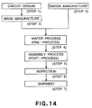
- Step 13 is a flow chart for explaining general procedure for manufacturing semiconductor devices.
- Step 1 is a design process for designing a circuit of a semiconductor device.
- Step 2 is a process for making a mask on the basis of the circuit pattern design.
- Step 3 is a process for preparing a wafer by using a material such as silicon.
- Step 4 is a wafer process which is called a pre-process wherein, by using the thus prepared mask and wafer, a circuit is formed on the wafer in practice, in accordance with lithography.
- Step 5 subsequent to this is an assembling step which is called a post-process wherein the wafer having been processed at step 4 is formed into semiconductor chips. This step includes an assembling (dicing and bonding) process and a packaging (chip sealing) process.
- Step 6 is an inspection step wherein an operation check, a durability check an so on, for the semiconductor devices produced by step 5, are carried out. With these processes, semiconductor devices are produced, and they are shipped (step 7).
- the step 4 described above includes an oxidation process for oxidizing the surface of a wafer; a CVD process for forming an insulating film on the wafer surface, an electrode forming process for forming electrodes upon the wafer by vapor deposition; an ion implanting process for implanting ions to the wafer; a resist process for applying a resist (photosensitive material) to the wafer; an exposure process for printing, by exposure, the circuit pattern of the mask on the wafer through the exposure apparatus described above; a developing process for developing the exposed wafer; an etching process for removing portions other than the developed resist image; and a resist separation process for separating the resist material remaining on the wafer after being subjected to the etching process. By repeating these processes, circuit patterns are superposedly formed on the wafer.
- the present invention can be applied to a vacuum-ambience exposure apparatus that does not use an electron beam, for example, an EUV exposure apparatus in which EUV (extreme ultraviolet) light is used as exposure light.
- EUV extreme ultraviolet
- the stage of the present invention can be used not only in a vacuum but also in a desired gas ambience.
Landscapes
- Engineering & Computer Science (AREA)
- Physics & Mathematics (AREA)
- General Physics & Mathematics (AREA)
- Epidemiology (AREA)
- Chemical & Material Sciences (AREA)
- Health & Medical Sciences (AREA)
- Environmental & Geological Engineering (AREA)
- Power Engineering (AREA)
- Public Health (AREA)
- Analytical Chemistry (AREA)
- Combustion & Propulsion (AREA)
- Electromagnetism (AREA)
- Exposure And Positioning Against Photoresist Photosensitive Materials (AREA)
- Electron Beam Exposure (AREA)
- Exposure Of Semiconductors, Excluding Electron Or Ion Beam Exposure (AREA)
- Container, Conveyance, Adherence, Positioning, Of Wafer (AREA)
Applications Claiming Priority (2)
| Application Number | Priority Date | Filing Date | Title |
|---|---|---|---|
| JP2003165512 | 2003-06-10 | ||
| JP2003165512A JP2005005393A (ja) | 2003-06-10 | 2003-06-10 | ステージ装置、露光装置、およびデバイス製造方法 |
Publications (2)
| Publication Number | Publication Date |
|---|---|
| EP1486829A2 true EP1486829A2 (de) | 2004-12-15 |
| EP1486829A3 EP1486829A3 (de) | 2006-08-30 |
Family
ID=33296823
Family Applications (1)
| Application Number | Title | Priority Date | Filing Date |
|---|---|---|---|
| EP04253447A Withdrawn EP1486829A3 (de) | 2003-06-10 | 2004-06-10 | Trägerplattensystem, Belichtungsanlage und Verfahren zur Herstellung einer Vorrichtung |
Country Status (3)
| Country | Link |
|---|---|
| US (2) | US7030964B2 (de) |
| EP (1) | EP1486829A3 (de) |
| JP (1) | JP2005005393A (de) |
Families Citing this family (13)
| Publication number | Priority date | Publication date | Assignee | Title |
|---|---|---|---|---|
| JP2005005393A (ja) * | 2003-06-10 | 2005-01-06 | Canon Inc | ステージ装置、露光装置、およびデバイス製造方法 |
| JP2005086029A (ja) * | 2003-09-09 | 2005-03-31 | Canon Inc | 位置決めステージ装置及び露光装置並びに半導体デバイスの製造方法 |
| JP4447949B2 (ja) * | 2004-03-25 | 2010-04-07 | キヤノン株式会社 | 位置決め装置の初期化方法、露光装置およびデバイス製造方法 |
| JP2005317916A (ja) * | 2004-03-30 | 2005-11-10 | Canon Inc | 露光装置及びデバイス製造方法 |
| JPWO2006006730A1 (ja) * | 2004-07-15 | 2008-05-01 | 株式会社ニコン | 平面モータ装置、ステージ装置、露光装置及びデバイスの製造方法 |
| JP2007312516A (ja) * | 2006-05-18 | 2007-11-29 | Canon Inc | 駆動装置、露光装置及びデバイス製造方法 |
| US7830046B2 (en) * | 2007-03-16 | 2010-11-09 | Nikon Corporation | Damper for a stage assembly |
| US7948337B2 (en) * | 2007-05-31 | 2011-05-24 | Seagate Technology Llc | Simultaneous rotational control using offset linear actuators |
| CN102422380A (zh) * | 2009-02-22 | 2012-04-18 | 迈普尔平版印刷Ip有限公司 | 带电粒子微影设备及真空腔室中产生真空的方法 |
| JP5917255B2 (ja) * | 2012-04-16 | 2016-05-11 | キヤノン株式会社 | 案内装置、露光装置および物品の製造方法 |
| JP5532175B1 (ja) * | 2013-07-02 | 2014-06-25 | 日本精工株式会社 | テーブル装置、及び搬送装置 |
| JP2016207756A (ja) * | 2015-04-17 | 2016-12-08 | 株式会社ニコン | ステージ装置及び露光装置 |
| CN112987512B (zh) * | 2021-03-08 | 2023-05-30 | 上海隐冠半导体技术有限公司 | 一种六自由度微动装置及电子束装备 |
Family Cites Families (18)
| Publication number | Priority date | Publication date | Assignee | Title |
|---|---|---|---|---|
| JP3182158B2 (ja) | 1991-02-25 | 2001-07-03 | キヤノン株式会社 | 露光装置用のステージ支持装置 |
| US5684856A (en) * | 1991-09-18 | 1997-11-04 | Canon Kabushiki Kaisha | Stage device and pattern transfer system using the same |
| JPH06183561A (ja) | 1992-12-18 | 1994-07-05 | Canon Inc | 移動ステージ装置 |
| JP3164960B2 (ja) | 1994-02-18 | 2001-05-14 | キヤノン株式会社 | ステージ装置 |
| JPH08229759A (ja) | 1995-02-24 | 1996-09-10 | Canon Inc | 位置決め装置並びにデバイス製造装置及び方法 |
| US5760564A (en) * | 1995-06-27 | 1998-06-02 | Nikon Precision Inc. | Dual guide beam stage mechanism with yaw control |
| JP3927620B2 (ja) | 1996-06-12 | 2007-06-13 | キヤノン株式会社 | 電子ビーム露光方法及びそれを用いたデバイス製造方法 |
| JP3907252B2 (ja) | 1996-12-05 | 2007-04-18 | キヤノン株式会社 | 露光装置およびデバイス製造方法ならびにステージ装置および原点出し方法 |
| JP3630964B2 (ja) | 1997-12-26 | 2005-03-23 | キヤノン株式会社 | ステージ装置、およびこれを用いた露光装置ならびにデバイス製造方法 |
| JPH11191585A (ja) | 1997-12-26 | 1999-07-13 | Canon Inc | ステージ装置、およびこれを用いた露光装置、ならびにデバイス製造方法 |
| US6144118A (en) * | 1998-09-18 | 2000-11-07 | General Scanning, Inc. | High-speed precision positioning apparatus |
| JP4474020B2 (ja) | 2000-06-23 | 2010-06-02 | キヤノン株式会社 | 移動装置及び露光装置 |
| DE50114723D1 (de) * | 2000-09-15 | 2009-04-09 | Vistec Electron Beam Gmbh | Sechsachsiges Positioniersystem mit magnetfeldfreiem Raum |
| JP2002252166A (ja) | 2001-02-27 | 2002-09-06 | Canon Inc | ステージ装置、露光装置およびデバイス製造方法ならびに移動案内方法 |
| US6788385B2 (en) * | 2001-06-21 | 2004-09-07 | Nikon Corporation | Stage device, exposure apparatus and method |
| JP2004055767A (ja) | 2002-07-18 | 2004-02-19 | Canon Inc | 電子ビーム露光装置及び半導体デバイスの製造方法 |
| JP3862639B2 (ja) | 2002-08-30 | 2006-12-27 | キヤノン株式会社 | 露光装置 |
| JP2005005393A (ja) * | 2003-06-10 | 2005-01-06 | Canon Inc | ステージ装置、露光装置、およびデバイス製造方法 |
-
2003
- 2003-06-10 JP JP2003165512A patent/JP2005005393A/ja active Pending
-
2004
- 2004-06-08 US US10/862,383 patent/US7030964B2/en not_active Expired - Fee Related
- 2004-06-10 EP EP04253447A patent/EP1486829A3/de not_active Withdrawn
-
2005
- 2005-11-30 US US11/289,472 patent/US20060082755A1/en not_active Abandoned
Also Published As
| Publication number | Publication date |
|---|---|
| US20060082755A1 (en) | 2006-04-20 |
| US7030964B2 (en) | 2006-04-18 |
| EP1486829A3 (de) | 2006-08-30 |
| JP2005005393A (ja) | 2005-01-06 |
| US20050018166A1 (en) | 2005-01-27 |
Similar Documents
| Publication | Publication Date | Title |
|---|---|---|
| US6867534B2 (en) | Low-mass and compact stage devices exhibiting six degrees of freedom of fine motion, and microlithography systems comprising same | |
| US7057193B2 (en) | Exposure apparatus | |
| US6930756B2 (en) | Electron beam exposure apparatus and semiconductor device manufacturing method | |
| US7365456B2 (en) | Positioning apparatus and charged-particle-beam exposure apparatus | |
| US7057710B2 (en) | Stage system including fine-motion cable unit, exposure apparatus, and method of manufacturing device | |
| US7030964B2 (en) | Stage system, exposure apparatus, and device manufacturing method | |
| US6128069A (en) | Stage mechanism for exposure apparatus | |
| US20080024749A1 (en) | Low mass six degree of freedom stage for lithography tools | |
| US6989888B2 (en) | Stage system, exposure apparatus, and device manufacturing method | |
| US20010046631A1 (en) | Divided reticles for charged-particle-beam microlithography apparatus, and methods for using same | |
| EP1398109B1 (de) | Trägervorrichtung und Antriebsverfahren, Belichtungsapparat und Herstellungsverfahren | |
| US6693284B2 (en) | Stage apparatus providing multiple degrees of freedom of movement while exhibiting reduced magnetic disturbance of a charged particle beam | |
| US11276558B2 (en) | Exposure apparatus and exposure method, lithography method, and device manufacturing method | |
| JP2005209709A (ja) | ステージ装置 | |
| JP2006287015A (ja) | 荷電粒子線露光装置 | |
| US7239051B2 (en) | Driving apparatus and exposure apparatus | |
| US6906334B2 (en) | Curved I-core | |
| US6794657B2 (en) | Magnetic shunt assembly for an exposure apparatus |
Legal Events
| Date | Code | Title | Description |
|---|---|---|---|
| PUAI | Public reference made under article 153(3) epc to a published international application that has entered the european phase |
Free format text: ORIGINAL CODE: 0009012 |
|
| AK | Designated contracting states |
Kind code of ref document: A2 Designated state(s): AT BE BG CH CY CZ DE DK EE ES FI FR GB GR HU IE IT LI LU MC NL PL PT RO SE SI SK TR |
|
| AX | Request for extension of the european patent |
Extension state: AL HR LT LV MK |
|
| PUAL | Search report despatched |
Free format text: ORIGINAL CODE: 0009013 |
|
| AK | Designated contracting states |
Kind code of ref document: A3 Designated state(s): AT BE BG CH CY CZ DE DK EE ES FI FR GB GR HU IE IT LI LU MC NL PL PT RO SE SI SK TR |
|
| AX | Request for extension of the european patent |
Extension state: AL HR LT LV MK |
|
| STAA | Information on the status of an ep patent application or granted ep patent |
Free format text: STATUS: THE APPLICATION HAS BEEN WITHDRAWN |
|
| 18W | Application withdrawn |
Effective date: 20061005 |