EP1487052A1 - Antennenanordnung in der Apertur einer elektrisch leitenden Fahrzeug-Karosserie - Google Patents
Antennenanordnung in der Apertur einer elektrisch leitenden Fahrzeug-Karosserie Download PDFInfo
- Publication number
- EP1487052A1 EP1487052A1 EP03001676A EP03001676A EP1487052A1 EP 1487052 A1 EP1487052 A1 EP 1487052A1 EP 03001676 A EP03001676 A EP 03001676A EP 03001676 A EP03001676 A EP 03001676A EP 1487052 A1 EP1487052 A1 EP 1487052A1
- Authority
- EP
- European Patent Office
- Prior art keywords
- aperture
- antenna
- capacitive
- low
- conductor
- Prior art date
- Legal status (The legal status is an assumption and is not a legal conclusion. Google has not performed a legal analysis and makes no representation as to the accuracy of the status listed.)
- Granted
Links
Images


Classifications
-
- H—ELECTRICITY
- H01—ELECTRIC ELEMENTS
- H01Q—ANTENNAS, i.e. RADIO AERIALS
- H01Q13/00—Waveguide horns or mouths; Slot antennas; Leaky-waveguide antennas; Equivalent structures causing radiation along the transmission path of a guided wave
- H01Q13/10—Resonant slot antennas
- H01Q13/103—Resonant slot antennas with variable reactance for tuning the antenna
-
- H—ELECTRICITY
- H01—ELECTRIC ELEMENTS
- H01Q—ANTENNAS, i.e. RADIO AERIALS
- H01Q1/00—Details of, or arrangements associated with, antennas
- H01Q1/12—Supports; Mounting means
- H01Q1/1271—Supports; Mounting means for mounting on windscreens
-
- H—ELECTRICITY
- H01—ELECTRIC ELEMENTS
- H01Q—ANTENNAS, i.e. RADIO AERIALS
- H01Q1/00—Details of, or arrangements associated with, antennas
- H01Q1/27—Adaptation for use in or on movable bodies
- H01Q1/32—Adaptation for use in or on road or rail vehicles
- H01Q1/325—Adaptation for use in or on road or rail vehicles characterised by the location of the antenna on the vehicle
- H01Q1/3275—Adaptation for use in or on road or rail vehicles characterised by the location of the antenna on the vehicle mounted on a horizontal surface of the vehicle, e.g. on roof, hood, trunk
Definitions
- the invention relates to an antenna arrangement in the substantially rectangular or. trapezoidal aperture 1 of an electrically conductive vehicle body in the meter wave range z. B. for FM reception.
- the invention is based on an antenna system as described, for example, in DE 195 35 250 A1 in Figure 4a using the example of a roof segment for a small vehicle.
- the antennas (5,6) specified there for frequencies up to the meter range are preferably designed as conductor structures made of thin wire. Due to the limited space available in vehicle construction, roof segments or segments in the conductive trunk lid are primarily suitable for the segments described there, the aperture length L being determined by the vehicle width and its aperture width B being determined by other vehicle-related framework conditions, such as the sunroof, rollover safety etc. is restricted. In the area of the meter waves in particular, this leads to the aperture length L often being less than half the operating wavelength and the aperture width B having to be selected to be less than 1/10 of the operating wavelength.
- the antennas (5, 6) proposed in DE 195 35 250 A1 in Fig. 4a cannot achieve the task of low-loss adaptation with the widest possible bandwidth.
- the object of the invention is therefore, in an antenna arrangement which in the preamble of Claim 1 specified type the disadvantage of the low-loss adaptation of the antenna to avoid given narrow band.
- This task is for an antenna arrangement in the preamble of claim 1 specified type with the help of the characterizing part of the main claim.
- the radiation associated with an antenna in an aperture of the specified type is at Aperture lengths noticeably below the half-wave resonance mainly due to the currents at. Aperture edge determined.
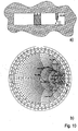
- an antenna of this type e.g. in the roof of a motor vehicle (Fig. 1a)
- Fig. 1a a motor vehicle
- the applicable directional diagram is independent of the shape for any excitation of the aperture the frequency, provided it does not exceed the aperture resonance.
- Antenna structures, which introduced into the aperture are therefore subject to their own frequencies at these frequencies Radiation contribution of the dominance of the edge currents given by the edge of the aperture. For this reason, it is necessary to structure the antenna structures introduced into the aperture in this way to design that the lowest possible loss and the possible bandwidth as little as possible reducing excitation of the edge currents of the aperture is given.
- An aperture of the type described has a high-pass similar in terms of its radiation properties Character, with frequencies above the aperture resonance in particular even with a wider aperture with different antenna structures and Positioning different radiation patterns and also relatively large bandwidths good efficiency can be achieved with relatively slim antenna conductors. This was in the Past based on numerous forms of window glass antennas in motor vehicles shown.
- the frequency dependence of the received voltage when illuminated in the main receiving direction is considered to be the effective height h eff in FIG. 2a.
- the maximum current occupancy is set at the natural resonance frequency f s of the aperture, which is expressed in a maximum value of the open circuit voltage measured at the coupling point, measured as the effective height.
- the resonance frequency results from the equality of the electrical power, that is the reactive power caused by the electric fields in the aperture with the magnetic power, that is the reactive power caused by the magnetic fields in the aperture.
- the reactive electrical power in the aperture is too small to cause the desired resonance-like edge currents.
- this deficit in reactive electrical power is eliminated by a capacitive tuning element 5, so that the resonant currents are now generated at a lower frequency F o , which is demonstrated by the resonant increase in the effective height in FIG. 2c.
- the capacitive tuning element 5 acts between the boundary points A and A ', the conductance G A indicated here in broken lines representing the effective radiation attenuation of the arrangement.
- the tuning measure with the effective capacitance ⁇ C c according to the invention is applied between the points C and C 'located in the middle of the aperture length.
- the effective capacitances are each represented by the series connection of an inductor L p or L pc and a capacitance C P or C pc .
- An essential element of the present invention consists in designing the effective capacitance at the selected location in the aperture to be extremely low-induction, that is to say with the smallest possible inductive influence. If the influence of the series inductance is negligible, the bandwidth of the resonance increase of the electrical and magnetic fields in the aperture is practically independent of the position d A for the attachment of the capacitive tuning element. In this case, the maximum relative bandwidth b ropt results at the frequency f o . If the inductive reactive power P mp in the element L p cannot be neglected in comparison to the magnetic reactive power P ma generated by the edge currents of the aperture, the relative bandwidth is reduced at the frequency f o to the value b ro approximately according to the following relationship:
- FIG. 4a shows the bandwidth reduction as a function of the influence of the unwanted magnetic reactive power occurring in L p as a function of the frequency ratio f o / f s for different values of C p / ⁇ C or P mp / P ma .
- the influence of the unwanted magnetic reactive power on the ratio of the relative bandwidth b ro at the frequency f o to the relative aperture bandwidth b rs at the natural resonance frequency f s is shown in FIG. 4b, taking into account that at low frequencies the optimally achievable bandwidth for the Current resonance becomes smaller with the third power of the frequency. It is all the more important not to reduce the bandwidth of the antenna arrangement by further disadvantageous coupling to the aperture.
- the capacitive tuning element must be designed according to the invention particularly free of induction, especially when tuning outside the center of the aperture. It is clear from the above explanations that a thin antenna conductor inserted into the aperture is not suitable for feeding the aperture 1 the reactive power ⁇ P e necessary for the tuning, since this is not possible without the bandwidth-reducing magnetic reactive power P mp due to its self-inductance.
- the invention is further explained using the example of an aperture 1 in a vehicle body 2 with an aperture length L of 90 cm and an aperture width B of 20 cm.
- the aim in this example is to create an antenna for an operating frequency range in accordance with the FM range, in Europe or in accordance with the FM frequency range in Japan.
- the conductance G o effective at this point (FIG. 3 b ) is approx. 1 mS without capacitive detuning in the case of the aperture resonance f s and is reduced to approx. 0.54 mS with the detuning considered to the resonance frequency f 0 .
- the relatively large reduction in the relative bandwidth b ro of the aperture resonance results for the specified detuning.
- the conductance of 0.54 mS corresponding to a resistance of 1.86 k ⁇ is too high a value in order to implement a simple lossless matching circuit. For this reason, it is technically much cheaper to position the coupling element 3 such that the impedance level available there is in the order of the desired antenna impedance, the conductance G in FIGS. 3a and 3b increasing as the distance d D from the center line of the aperture 1 increases increases rapidly. This impedance level is determined by the conductance G in FIG.
- This transformation which is to be regarded as a practically loss-free measure, enables, for example, the design of an equivalent resonance band filter with two resonance circuits, as is shown in FIG. 6a.
- the aperture 1 acts as a resonance circuit tuned to the frequency f o .
- the broadband impedance curve shown in FIG. 6b can be generated with little loss.
- the aperture resonance can be produced equivalent in different ways without that here the coupling element 3, apart from fine-tuning measures, changed should be.
- the low inductance conductor 9 is as flat conductor with a sufficiently large conductor width 11 executed.
- the capacitive tuning element 5 with the desired effective capacitance ⁇ C is the configuration of the interruption point 6 as a slot capacitance, which can be set by selecting a suitable conductor slot width 14.
- FIG. 7 a an impedance curve that is completely equivalent to FIG. 6 b can be achieved for the predetermined frequency range with a practically unchanged design of the coupling element 3.
- the tuning measure is applied in the center line as in FIG. 3b, the influence of the conductor inductance L pc is small enough to be able to use conductors with an advantageously small cross-section for space reasons, as in FIG. 6a. This is evident from the equivalence of the impedance curves in FIGS. 6b and 7b.
- FIG. 5a A further advantageous possibility of designing the capacitive tuning element 5 is shown in FIG. 5a.
- the capacitive tuning element 5 is introduced into the aperture 1 at a significant distance d A.
- the influence of inductance L p is significantly greater than that of an inductor L pc of the same size for central attachment (see Eq. 11).
- a flat design of the low-inductance conductor 9 is therefore advantageous.
- the capacitive component 7 when introducing concentrated capacitive components 12 with a predetermined edge distance 10 or with a suitable choice of a conductor slot width 14 with the sufficiently large conductor width 11
- the impedance curve shown in FIG. 5b can be achieved.
- the comparison of the impedance curves in FIGS. 6b, 7b and 5b shows that all the options for tuning the aperture resonance shown in FIGS. 6a, 7a and 5a are practically equivalent.
- the capacitive tuning element 5 as a larger conductive surface 17 with a longitudinal dimension up to half an aperture length L introduced into the aperture 1 as a low-inductance conductor 9, as in FIG. 8a.
- the desired capacitive overall effect is due to the edge distance 10 between the edges conductive surface 17 and the aperture edges 13 in connection with suitable distributed arranged concentrated capacitive components 12 designed.
- the conductive Surface 17 of the capacitive tuning element 5 for receiving further antennas for others
- To design frequency ranges like a trough This trough can advantageously be used as a conductive one Base area 25 can be designed by microwave antennas 24 (FIG. 8c).
- To bring out the Connection lines from aperture 1 are fed through for the meter wave frequency range Throttling designed with high resistance.
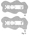
- the coupling element 3 with its antenna connection point 4 for coupling to the resonance-like excessive magnetic field or to the resonance-like excessive electric field in the aperture 1, can with a coupling element 3 with the character of a magnetic dipole 20 or with a coupling element 3 with the character of an electrical dipole 26 (Fig. 11 a, Fig. 11b).
- Magnetically acting coupling element 3 for decoupling the strong magnetic Fields at the end of aperture 1 are additionally shown in FIGS. 2b, 2d and 3a, 3b, 3c.
- the Coupling with an electrical monopole is shown in Fig. 8a.
- the associated one Impedance curve in Fig. 8a shows the broadband nature of this arrangement
- Antenna connection point 4 which advantageously transforms into the desired one Impedance curve in FIG. 9b with the simple, low-loss blind elements indicated in FIG. 9a allows.
- a particularly advantageous coupling to the aperture 1 is the capacitive mentioned above Coupling for the design of an equivalent resonance band filter with two circles, as shown in Figures 5a, 6a and 7a is shown.
- a particularly advantageous variant of the design the coupling element 3 with regard to the design of combination antennas is in Fig. 10a shown.
- the capacitive Tuning element 5 are advantageously attached in the region of the center of the aperture 1 and low inductance conductor 9 contain several interruption points 6, as indicated in Fig. 5c. As a result, the shielding effect on an adjacent LMK receiving antenna element 15 becomes common its LMK junction 16 significantly reduced.
- the Coordination is carried out by suitable design of the edge distance 10 in connection with the distributed introduction of concentrated capacitive components 12. Due to the increased The concentration of the magnetic fields in the immediate vicinity is not too small Edge distance 10 hardly an adverse decrease in the self-inductance as a magnetic Energy storage connected to the aperture.
- the desired antenna impedance can, if appropriate Positioning of the antenna connection point 4 can be set. This impedance is in Fig. 12b shown and shows a broadband loop in the frequency range of 80 to 110 MHz.
- Typical circuit measures can transform such a broadband impedance into a desired one Impedance curve e.g. be transformed for the FM range.
Landscapes
- Engineering & Computer Science (AREA)
- Remote Sensing (AREA)
- Details Of Aerials (AREA)
Abstract
Description
- Fig. 1a)
- Aussparung mit der Aperturlänge L und der Aperturbreite B im leitenden Dach eines Kfz zur Bildung einer Antenne nach der Erfindung
- Fig. 1b)
- azimutales Strahlungsdiagramm bei Horizontalpölarisation bei Frequenzen unterhalb der Apertur-Eigenresonanz
- Fig. 2a)
- Frequenzverlauf der Leerlauf-Empfangsspannung am Ankoppelelement 3 zum Nachweis der Eigenresonanzfrequenz fs der Apertur
- Fig. 2b)
- Anordnung zur Feststellung der Eigenresonanzfrequenz fs
- Fig. 2c)
- Frequenzverlauf der Leerlauf Empfangsspannung einer Antenne nach der Erfindung am Ankoppelelement 3 zum Nachweis der durch Verstimmung reduzierten Resonanzfrequenz fo
- Fig. 2b)
- Antenne nach der Erfindung mit einer auf die niedrigere Resonanzfrequenz fo abgestimmten Apertur mit dem kapazitiven Abstimmelement 5
- Fig. 3 a) und b)
- Ersatzschaltbilder zur Erläuterung der die Bandbreite reduzierenden Wirkung
einer induktiven Komponente im kapazitiven Abstimmelement 5.
c) verlustlose Impedanztransformation auf das gewünschte Impedanzniveau bei Frequenzen unterhalb der Eigenresonanz der Apertur. - Fig. 4
- Reduzierung der Bandbreite in Abhängigkeit von der Verstimmung fo/fs bei verschiedenen
unerwünschten induktiven Effekten im kapazitiven Abstimmelement 5 als Parameter
a) Verhältnis von bro mit induktivem Effekt zu bropt ohne induktiven Effekt jeweils bei fo
b) Verhältnis von bro bei fo mit induktivem Effekt zu brs bei der Apertur-Eigenresonanz fs - Fig. 5
- a) Realisierung eines kapazitiven Abstimmelements 5 mit induktivitätsarmem Leiter 9 und
Ankoppelelement 3 mit kapazitiver Ankopplung 23 und Parallelresonanzkreis 21 zur
Gestaltung eines Zweikreis- Resonanzbandfilter -Verhaltens
b) Antennenimpedanz an der Antennenanschlußstelle 4 in a) für den FM-Bereich in Japan
c) Induktivitätsarmer Leiter 9 mit Unterbrechungsstellen zur Verminderung der Abschirmwirkung eines benachbarten LMK-Empfangsantennenelements 15 mit LMK-Anschlußstelle 16 - Fig. 6
- a) Realisierung eines kapazitiven Abstimmelements 5 mit kleinem Kapazitätswert 7 bei
mittiger Anbringung in der Apertur 1
b) Nachweis der Gleichwertigkeit der Abstimmung auf die gleiche Resonanzfrequenz fo der Apertur wie in.Fig. 5a zur Gestaltung des ähnlichen Impedanzverlaüfs wie in Fig.5b mit der Anordnung in a) - Fig. 7
- a) Wie Fig. 6a jedoch mit breiterem kapazitätsarmen Leiter 9
b) Impedanzverlauf für die Anordnung in a) ähnlich wie in Fig. 6b - Fig. 8
- Nachweis der Breitbandigkeit auch bei größerer Bedeckung der Aperturlänge L mit
einem induktivitätsarmen Leiter
a) Anordnung des induktivitätsarmen Leiters 9 mit kapazitiven Bauelementen 12 und von ihm getrenntem kapazitiven Koppelelement 3 mit Antennenanschlussstelle 4
b) Impedanzverlauf für die Anordnung in a) an der, Antennenanschlussstelle 4
c) wannenartig ausgebildeter induktivitätsarmer Leiter 9 mit Dielektrikum εr zur Ausbildung der zur Abstimmung benötigten verteilten Kapazität zwischen Wannenrand 19 und Aperturrand 13. Die Mikrowellenantenne 24 nutzt die Wanne als Grundfläche - Fig. 9
- a) Anordnung wie in Fig. 8a, jedoch mit kapazitivem Ankoppelelement 3 mit einer
einfachen Transformationsschaltung
b) Impedanzverlauf für die Anordnung in a) an der Antennenanschlussstelle 4 für das UKW-Band als Betriebsfrequenzbereich - Fig. 10
- a) Anordnung ähnlich wie in Fig. 7a jedoch mit galvanisch mit der Fahrzeugkarosserie
verbundenen flächigem Leiter 22 als mögliche leitende Grundfläche 25 für eine
Mikrowellenantenne bei einem kombinierten Antennensystem
b) Impedanzverlauf für die Anordnung in a) an der Antennenanschlussstelle 4 für das FM- Band in Japan als Betriebsfrequenzbereich - Fig. 11
- Grundformen für die Ausbildung von Ankoppelelementen 3
a) als magnetischer Dipol 20
b) als elektrischer Dipol 26 - Fig. 12
- Nachweis der Breitbandigkeit auch bei nahezu über die gesamte Aperturlänge L
eingebrachte leitende Fläche 17 als induktivitätsarmer Leiter 9 bei kombinierter
Verwendung als Ankoppelelement 3 mit Antennenanschlussstelle 4
a) Anordnung
b) Impedanzverlauf für die Anordnung in a) zur anschließend breitbandigen Transformation für den UKW-Bereich

Claims (16)
- Antennenanordnung in der im wesentlichen rechteck-bzw. trapezförmigen Apertur (1) mit der Aperturlänge L und der Aperturbreite B mit B < L/3 einer elektrisch leitenden Fahrzeugkarosserie (2) im Meterwellenbereich
dadurch gekennzeichnet, dass
die Aperturlänge L so klein gewählt ist, dass die Eigenresonanzfrequenz (fs) der Apertur (1) größer ist als die Mittenfrequenz des Betriebsfrequenzbereichs und ein kapazitives Abstimmelement (5) zur Abstimmung der Aperturresonanz auf eine Resonanzfrequenz fo in der Nähe dieser Mittenfrequenz und ein Ankoppelelement (3) zur Ankopplung der Antennenanschlussstelle (4) an die resonanzartig überhöhten elektromagnetischen. Felder in der Apertur (1) vorhanden sind und das kapazitive Abstimmelement (5) als kapazitiv wirkende Verbindung zwischen Rändern der Apertur (1) eingebracht ist und derart induktivitätsarm gestaltet ist, dass die durch die verbleibende induktive Wirkung auftretende magnetische Blindleistung (Pmp) möglichst klein ist im Vergleich zur magnetischen, von den magnetischen Feldern in der Apertur (1) erzeugten Blindleistung (Pma). - Antennenanordnung nach Anspruch 1
dadurch gekennzeichnet, dass
ein kapazitives Abstimmelement (5) als kapazitiv wirkende Verbindung zwischen einander gegenüberliegenden Punkten (A, A') auf den Längsrändem der Apertur (1) in einem ersten Abstand (dA) eingebracht ist und die Distanz (8) zwischen diesen Punkten mit einem induktivitätsarmen Leiter (9) überbrückt ist, welcher mindestens an einer Unterbrechungsstelle (6) aufgetrennt ist und an jeder Unterbrechungsstelle (6) zur Überbrückung derselben jeweils ein kapazitives Bauelement (7) vorhanden ist, dessen Kapazitätswert so groß gewählt ist, dass in der Gesamtwirkung die Lieferung der zur Abstimmung der Apertur (1) auf die gewünschte Resonanzfrequenz fo notwendigen elektrische Blindleistung Pe gegeben ist. - Antennenanordnung nach einem der Ansprüche 1 bis 2
dadurch gekennzeichnet, dass
insbesondere für größere Werte des ersten Abstand (dA) der induktivitätsarme Leiter (9) als flächiger Leiter mit einer hinreichend großen Leiterbreite (11) ausgeführt ist und zur induktionsarmen kapazitiven Überbrückung der Unterbrechungsstelle (6) bzw. der Unterbrechungsstellen (6) jeweils eines bzw. mehrere über die Leiterbreite (11) verteilte, konzentrierte kapazitive Bauelemente (12) verwendet sind (Fig. 5a). - Antennenanordnung nach einem der Ansprüche 1 bis 3
dadurch gekennzeichnet, dass
nur eine Unterbrechungsstelle (6) vorhanden ist, welche an einem der Aperturränder (13)gegeben ist, sodass die gesamte Fläche des induktivitätsarmen Leiters (9) galvanisch mit der Fahrzeugkarosserie (2) verbunden ist (Fig. 5a). - Antennenanordnung nach einem der Ansprüche 1 bis 4
dadurch gekennzeichnet, dass
die Unterbrechungsstelle (6) bzw. die Unterbrechungsstellen (6) des flächenhaft ausgebildeten induktivitätsarmen Leiters (9) als Schlitze mit einer geeigneten Leiterschlitzweite (14) im Hinblick auf die zwischen den Schlitzrändern wirksame Schlitzkapazität derart gestaltet sind, dass bei der gewählten Leiterbreite (11) die geforderte kapazitive Wirkung gegeben ist (Fig. 5a,c) - Antennenanordnung nach einem der Ansprüche 1 bis 4
dadurch gekennzeichnet, dass
zur Gestaltung des kapazitiven Abstimmelements (5) der induktivitätsarme Leiter (9) als eine leitende Fläche 17 über einen größeren Teil der Aperturlänge L in die Apertur 1 eingebracht ist und die Abstimmung durch geeignete Gestaltung des Randabstand 10 in Verbindung mit verteilten konzentrierten kapazitiven Bauelementen 12 gegeben ist und der induktivitätsarme Leiter (9) kombiniert als Ankoppelelement 3 verwendet ist (Fig. 12b). - Antennenanordnung nach einem der Ansprüche 1 bis 3
dadurch gekennzeichnet, dass
zur Gestaltung des kapazitiven Abstimmelements (5) mit einem im Sinne der Erfindung induktivitätsarmen Leiter (9) mit kleinen Querschnittsabmessungen in der Nähe der Mitte der Aperturlänge L eingebracht ist und die kapazitive Wirkung durch die Einbringung eines konzentrierten kapazitiven Bauelements (7) bzw. durch die Einbringung mehrerer konzentrierter kapazitiver Bauelemente (7) bei Vorhandensein mehrerer Unterbrechungsstellen gegeben ist (Fig. 6a). - Antennenanordnung nach einem der Ansprüche 1 bis 4
dadurch gekennzeichnet, dass
zur Gestaltung des kapazitiven Abstimmelements (5) eine größere leitende Fläche (17) mit einer Längsabmessung bis zu einer halben Aperturlänge L als induktivitätsarmer Leiter (9) in die Apertur (1) eingebracht ist und die Unterbrechungsstellen (6) durch den Abstand zwischen der Berandung dieser leitenden Fläche (17) und den Aperturrändem (13) gegeben ist und die geeignete kapazitive Gesamtwirkung durch induktionsarme Überbrückung mit mehreren verteilt angeordnete konzentrierten kapazitive Bauelementen (12) gegeben ist (Fig.8a). - Antennenanordnung nach einem der Ansprüche 1 bis 6
dadurch gekennzeichnet, dass
die leitende Fläche (17) zur Gestaltung des kapazitiven Abstimmelements (5) wannenartig ausgebildet ist und die Unterbrechungsstellen (6) als laufender dielektrisch isolierter Spalt (18) zwischen dem Wannenrand (19) und dem Aperturrand (13) gegeben ist und der Spalt (18) durch Formgebung und durch Ausfüllung mit einem geeigneten dielektrischen Material derart ausgebildet ist, daß die Abstimmung der Aperturresonanz auf die gewünschte Resonanzfrequenz fo gegeben ist (Fig.8c). - Antennenanordnung nach einem der Ansprüche 1 bis 9
dadurch gekennzeichnet, dass
das Ankoppelelement (3) zur vorwiegenden Ankopplung an das resonanzartig überhöhte magnetische Feld als ein Antennenelement mit dem Charakter eines magnetischen Dipols (20) derart gestaltet und in der Apertur derart positioniert ist, dass an der Antennenanschlussstelle (4) im vorgegebenen Betriebsfrequenzbereich ein Antennenimpedanzverlauf mit einem auf den gewünschten Impedanzwert bezogenen ausreichend kleinen Betrag des Reflexionsfaktors vorliegt, sodass dieser Antennenimpedanzverlauf praktisch verlustfrei und ohne die Bandbreite einschränkende Wirkung mit Hilfe konzentrierter Blindelemente an den gewünschten Impedanzwert angepasst werden kann. (Fig. 11a, 3a, 3b) - Antennenanordnung nach einem der Ansprüche 1 bis 9
dadurch gekennzeichnet, dass das Ankoppelelement (3) zur vorwiegenden Ankopplung an das resonanzartig überhöhte elektrische Feld als ein Antennenelement mit dem Charakter eines elektrischen Dipols (26) derart gestaltet und in der Apertur derart positioniert ist, dass an der Antennenanschlussstelle (4) im vorgegebenen Betriebsfreqüenzbereich ein Antennenimpedanzverlauf mit einem auf den gewünschten Impedanzwert bezogenen ausreichend kleinen Betrag des Reflexionsfaktors vorliegt, sodass dieser Antennenimpedanzverlauf praktisch verlustfrei und ohne die Bandbreite einschränkende Wirkung mit Hilfe konzentrierter Blindelemente an den gewünschten Impedanzwert angepasst werden kann. - Antennenanordnung nach einem der Ansprüche 1 bis 9
dadurch gekennzeichnet, dass
das Ankoppelelement (3) im wesentlichen als gestreckter Leiter ausgeführt ist und mit seiner Antennenanschlussstelle (4) zwischen zwei einander gegenüberliegenden Punkten der Aperturränder (13) im Abstand dD von der Mitte der Aperturlänge L eingebracht ist und dieser Abstand dD zur Erreichung eines hinreichend niedrigen Impedanzniveaus entsprechend groß gewählt ist und das Ankoppelelement (3) eine serielle Ankoppelkapazität enthält zur Ankopplung an die Apertur (1) als ersten Resonanzkreis eines kapazitiv gekoppelten. Zweikreisbandfilters und der zweite Resonanzkreis des Zweikreisbandfilters durch verlustarme Blindelemente (21) parallel zur Antennenanschlussstelle (4) gebildet ist (Fig.5a, 6a, 7a). - Antennenanordnung nach Anspruch 12
dadurch gekennzeichnet, dass
im Ankoppelelement (3) zusätzlich eine Serieninduktivität (26) enthalten ist, mit deren Induktivitätswert in Verbindung mit der Ankoppelkapazität (23) und den verlustarmen Blindelementen (21) ein die Bandbreite vergrößerndes Dreikreisbandfilter gegeben ist. - Antennenanordnung nach Anspruch 12
dadurch gekennzeichnet, dass
der im wesentlichen gestreckte Leiter (22) im Ankoppelelement (3) an seinem einen Ende mit einem Aperturrand (13) galvanisch verbunden und zum Zwecke der Verwendung als leitende Grundfläche (25) von Mikrowellenantennen (24) für um Größenordnungen höhere Frequenzen flächenhaft gestaltet sind (Fig. 10). - Antennenanordnung nach einem der Ansprüche 1 bis 6 und 8 bis 14
dadurch gekennzeichnet, dass
die leitende Fläche (17) zur Gestaltung des kapazitiven Abstimmelements (5) zum Zwecke der zusätzlichen Verwendung als leitende Grundfläche (25) von Mikrowellenantennen (24) für um Größenordnungen höhere Frequenzen gestaltet ist und die Anschlussleitungen der Mikrowellenantennen (24) zur Herausführung aus der Apertur (1) für den Meterwellenfrequenzbereich durch Verdrosselung hochohmig gestaltet ist (Fig.9). - Antennenanordnung nach einem der Ansprüche 1 bis 3, 5, 6 und 8 bis 14
dadurch gekennzeichnet, dass
in der Apertur (1) ein kapazitives LMK-Empfangsantennenelement (15) vorhanden ist und die abschirmende Wirkung des induktivitätsarmen Leiters (9) bezüglich des Empfangs der niedrigen LMK-Frequenzen durch die Ausgestaltung mit mehreren Unterbrechungsstellen (6) weitgehend aufgehoben ist (Fig. 5c).
Priority Applications (3)
| Application Number | Priority Date | Filing Date | Title |
|---|---|---|---|
| DE50312708T DE50312708D1 (de) | 2003-01-25 | 2003-01-25 | Antennenanordnung in der Apertur einer elektrisch leitenden Fahrzeug-Karosserie |
| EP03001676A EP1487052B1 (de) | 2003-01-25 | 2003-01-25 | Antennenanordnung in der Apertur einer elektrisch leitenden Fahrzeug-Karosserie |
| AT03001676T ATE467922T1 (de) | 2003-01-25 | 2003-01-25 | Antennenanordnung in der apertur einer elektrisch leitenden fahrzeug-karosserie |
Applications Claiming Priority (1)
| Application Number | Priority Date | Filing Date | Title |
|---|---|---|---|
| EP03001676A EP1487052B1 (de) | 2003-01-25 | 2003-01-25 | Antennenanordnung in der Apertur einer elektrisch leitenden Fahrzeug-Karosserie |
Publications (2)
| Publication Number | Publication Date |
|---|---|
| EP1487052A1 true EP1487052A1 (de) | 2004-12-15 |
| EP1487052B1 EP1487052B1 (de) | 2010-05-12 |
Family
ID=33185842
Family Applications (1)
| Application Number | Title | Priority Date | Filing Date |
|---|---|---|---|
| EP03001676A Expired - Lifetime EP1487052B1 (de) | 2003-01-25 | 2003-01-25 | Antennenanordnung in der Apertur einer elektrisch leitenden Fahrzeug-Karosserie |
Country Status (3)
| Country | Link |
|---|---|
| EP (1) | EP1487052B1 (de) |
| AT (1) | ATE467922T1 (de) |
| DE (1) | DE50312708D1 (de) |
Cited By (3)
| Publication number | Priority date | Publication date | Assignee | Title |
|---|---|---|---|---|
| WO2017211536A1 (de) * | 2016-06-07 | 2017-12-14 | Audi Ag | Kraftfahrzeug mit antennenanordnung |
| DE102016009712A1 (de) | 2016-08-10 | 2018-02-15 | Heinz Lindenmeier | Aktive Antennenanordnung für den Rundfunkempfang im Ausschnitt einer elektrisch leitenden Fahrzeugkarosserie |
| CN113169453A (zh) * | 2018-11-29 | 2021-07-23 | Zn 科技株式会社 | 用于节能的电磁耦合装置及包括其的无线通信系统 |
Citations (5)
| Publication number | Priority date | Publication date | Assignee | Title |
|---|---|---|---|---|
| US3210766A (en) | 1962-02-15 | 1965-10-05 | Ralph O Parker | Slot type antenna with tuning circuit |
| US4003056A (en) * | 1975-05-20 | 1977-01-11 | Ross Alan Davis | Windshield antenna system with resonant element and cooperating resonant conductive edge |
| US5138330A (en) * | 1989-03-08 | 1992-08-11 | Hans Kolbe & Co. Nachrichtenubertragungstechnik | Pane antenna having an amplifier |
| US5465098A (en) * | 1991-11-05 | 1995-11-07 | Seiko Epson Corporation | Antenna apparatus for transceiver |
| DE19535250A1 (de) | 1995-09-22 | 1997-03-27 | Fuba Automotive Gmbh | Mehrantennensystem für Kraftfahrzeuge |
-
2003
- 2003-01-25 AT AT03001676T patent/ATE467922T1/de not_active IP Right Cessation
- 2003-01-25 EP EP03001676A patent/EP1487052B1/de not_active Expired - Lifetime
- 2003-01-25 DE DE50312708T patent/DE50312708D1/de not_active Expired - Lifetime
Patent Citations (5)
| Publication number | Priority date | Publication date | Assignee | Title |
|---|---|---|---|---|
| US3210766A (en) | 1962-02-15 | 1965-10-05 | Ralph O Parker | Slot type antenna with tuning circuit |
| US4003056A (en) * | 1975-05-20 | 1977-01-11 | Ross Alan Davis | Windshield antenna system with resonant element and cooperating resonant conductive edge |
| US5138330A (en) * | 1989-03-08 | 1992-08-11 | Hans Kolbe & Co. Nachrichtenubertragungstechnik | Pane antenna having an amplifier |
| US5465098A (en) * | 1991-11-05 | 1995-11-07 | Seiko Epson Corporation | Antenna apparatus for transceiver |
| DE19535250A1 (de) | 1995-09-22 | 1997-03-27 | Fuba Automotive Gmbh | Mehrantennensystem für Kraftfahrzeuge |
Cited By (5)
| Publication number | Priority date | Publication date | Assignee | Title |
|---|---|---|---|---|
| WO2017211536A1 (de) * | 2016-06-07 | 2017-12-14 | Audi Ag | Kraftfahrzeug mit antennenanordnung |
| US10270178B2 (en) | 2016-06-07 | 2019-04-23 | Audi Ag | Motor vehicle having an antenna arrangement |
| DE102016009712A1 (de) | 2016-08-10 | 2018-02-15 | Heinz Lindenmeier | Aktive Antennenanordnung für den Rundfunkempfang im Ausschnitt einer elektrisch leitenden Fahrzeugkarosserie |
| WO2018029273A1 (de) | 2016-08-10 | 2018-02-15 | Fuba Automotive Electronics Gmbh | Aktive antennenanordnung für den rundfunkempfang im ausschnitt einer elektrisch leitenden fahrzeugkarosserie |
| CN113169453A (zh) * | 2018-11-29 | 2021-07-23 | Zn 科技株式会社 | 用于节能的电磁耦合装置及包括其的无线通信系统 |
Also Published As
| Publication number | Publication date |
|---|---|
| DE50312708D1 (de) | 2010-06-24 |
| ATE467922T1 (de) | 2010-05-15 |
| EP1487052B1 (de) | 2010-05-12 |
Similar Documents
| Publication | Publication Date | Title |
|---|---|---|
| EP0155647B1 (de) | Antennenanordnung in der Heckscheibe eines Kraftfahrzeugs | |
| EP2256673B1 (de) | RFID-Transponder zur Montage auf Metall und Herstellungsverfahren für denselben | |
| EP0594809B1 (de) | Funkantennenanordnung in der nähe von fahrzeug-fensterscheiben | |
| DE69409447T2 (de) | Antenne für Mobilfunk | |
| DE102007061305B4 (de) | Mehrteilige Antenne mit zirkularer Polarisation und Funkstation | |
| EP1154518B1 (de) | Integrierte Antenne für Mobilfunktelefone | |
| DE10030489B4 (de) | Kapazitives Erdungssystem für VHF- und UHF-Antennen | |
| DE2911885A1 (de) | Ortsveraenderbare uebertragungs-antennenanordnung | |
| DE102014225717A1 (de) | Zweiband-PCB-Antenne für ein Fahrzeug | |
| DE69913962T2 (de) | Mehrband-fahrzeugantenne | |
| DE69811966T2 (de) | Antennenvorrichtung | |
| DE112019000636T5 (de) | Antennenvorrichtung, Fensterscheibe für ein Fahrzeug und Fensterscheibenstruktur | |
| EP2693565A1 (de) | Elektrischer Strahler für vertikal polarisierte Funksignale | |
| DE2136759C2 (de) | Antenne mit metallischem Rahmen und den Rahmen erregendem Unipol | |
| DE4443596B4 (de) | Funkantenne auf der Fensterscheibe eines Kraftfahrzeugs | |
| DE10141583B4 (de) | Antennenanordnung in der Apertur einer elektrisch leitenden Fahrzeugkarosserie | |
| WO2003052873A1 (de) | Hohlraumresonatorantenne mit breitbandschlitz | |
| EP1487052B1 (de) | Antennenanordnung in der Apertur einer elektrisch leitenden Fahrzeug-Karosserie | |
| DE102014016851B3 (de) | MIMO Schlitzantenne für Kraftfahrzeuge | |
| DE3630519C2 (de) | ||
| DE60007254T2 (de) | Planare Antenne für Motorfahrzeuge | |
| WO2004102742A1 (de) | Mehrbandfähige antenne | |
| DE3410950A1 (de) | Antennenanordnung, insbesondere fuer kraftfahrzeuge | |
| DE102016109156B4 (de) | Strahlereinheit und Antennenanordnung, insbesondere für ein Kraftfahrzeug mit einer solchen Strahlereinheit | |
| DE3420046C2 (de) |
Legal Events
| Date | Code | Title | Description |
|---|---|---|---|
| PUAI | Public reference made under article 153(3) epc to a published international application that has entered the european phase |
Free format text: ORIGINAL CODE: 0009012 |
|
| AK | Designated contracting states |
Kind code of ref document: A1 Designated state(s): AT BE BG CH CY CZ DE DK EE ES FI FR GB GR HU IE IT LI LU MC NL PT SE SI SK TR |
|
| AX | Request for extension of the european patent |
Extension state: AL LT LV MK RO |
|
| 17P | Request for examination filed |
Effective date: 20050112 |
|
| 17Q | First examination report despatched |
Effective date: 20050307 |
|
| AKX | Designation fees paid |
Designated state(s): AT BE BG CH CY CZ DE DK EE ES FI FR GB GR HU IE IT LI LU MC NL PT SE SI SK TR |
|
| RAP1 | Party data changed (applicant data changed or rights of an application transferred) |
Owner name: DELPHI DELCO ELECTRONICS EUROPE GMBH |
|
| RAP1 | Party data changed (applicant data changed or rights of an application transferred) |
Owner name: DELPHI DELCO ELECTRONICS EUROPE GMBH |
|
| GRAP | Despatch of communication of intention to grant a patent |
Free format text: ORIGINAL CODE: EPIDOSNIGR1 |
|
| GRAS | Grant fee paid |
Free format text: ORIGINAL CODE: EPIDOSNIGR3 |
|
| GRAA | (expected) grant |
Free format text: ORIGINAL CODE: 0009210 |
|
| AK | Designated contracting states |
Kind code of ref document: B1 Designated state(s): AT BE BG CH CY CZ DE DK EE ES FI FR GB GR HU IE IT LI LU MC NL PT SE SI SK TR |
|
| REG | Reference to a national code |
Ref country code: GB Ref legal event code: FG4D Free format text: NOT ENGLISH |
|
| REG | Reference to a national code |
Ref country code: CH Ref legal event code: EP |
|
| REG | Reference to a national code |
Ref country code: IE Ref legal event code: FG4D Free format text: LANGUAGE OF EP DOCUMENT: GERMAN |
|
| REF | Corresponds to: |
Ref document number: 50312708 Country of ref document: DE Date of ref document: 20100624 Kind code of ref document: P |
|
| REG | Reference to a national code |
Ref country code: NL Ref legal event code: VDEP Effective date: 20100512 |
|
| PG25 | Lapsed in a contracting state [announced via postgrant information from national office to epo] |
Ref country code: NL Free format text: LAPSE BECAUSE OF FAILURE TO SUBMIT A TRANSLATION OF THE DESCRIPTION OR TO PAY THE FEE WITHIN THE PRESCRIBED TIME-LIMIT Effective date: 20100512 Ref country code: ES Free format text: LAPSE BECAUSE OF FAILURE TO SUBMIT A TRANSLATION OF THE DESCRIPTION OR TO PAY THE FEE WITHIN THE PRESCRIBED TIME-LIMIT Effective date: 20100823 Ref country code: SE Free format text: LAPSE BECAUSE OF FAILURE TO SUBMIT A TRANSLATION OF THE DESCRIPTION OR TO PAY THE FEE WITHIN THE PRESCRIBED TIME-LIMIT Effective date: 20100512 |
|
| PG25 | Lapsed in a contracting state [announced via postgrant information from national office to epo] |
Ref country code: FI Free format text: LAPSE BECAUSE OF FAILURE TO SUBMIT A TRANSLATION OF THE DESCRIPTION OR TO PAY THE FEE WITHIN THE PRESCRIBED TIME-LIMIT Effective date: 20100512 Ref country code: SI Free format text: LAPSE BECAUSE OF FAILURE TO SUBMIT A TRANSLATION OF THE DESCRIPTION OR TO PAY THE FEE WITHIN THE PRESCRIBED TIME-LIMIT Effective date: 20100512 |
|
| REG | Reference to a national code |
Ref country code: IE Ref legal event code: FD4D |
|
| PG25 | Lapsed in a contracting state [announced via postgrant information from national office to epo] |
Ref country code: GR Free format text: LAPSE BECAUSE OF FAILURE TO SUBMIT A TRANSLATION OF THE DESCRIPTION OR TO PAY THE FEE WITHIN THE PRESCRIBED TIME-LIMIT Effective date: 20100813 Ref country code: CY Free format text: LAPSE BECAUSE OF FAILURE TO SUBMIT A TRANSLATION OF THE DESCRIPTION OR TO PAY THE FEE WITHIN THE PRESCRIBED TIME-LIMIT Effective date: 20100512 |
|
| PG25 | Lapsed in a contracting state [announced via postgrant information from national office to epo] |
Ref country code: DK Free format text: LAPSE BECAUSE OF FAILURE TO SUBMIT A TRANSLATION OF THE DESCRIPTION OR TO PAY THE FEE WITHIN THE PRESCRIBED TIME-LIMIT Effective date: 20100512 Ref country code: EE Free format text: LAPSE BECAUSE OF FAILURE TO SUBMIT A TRANSLATION OF THE DESCRIPTION OR TO PAY THE FEE WITHIN THE PRESCRIBED TIME-LIMIT Effective date: 20100512 Ref country code: IE Free format text: LAPSE BECAUSE OF FAILURE TO SUBMIT A TRANSLATION OF THE DESCRIPTION OR TO PAY THE FEE WITHIN THE PRESCRIBED TIME-LIMIT Effective date: 20100512 Ref country code: PT Free format text: LAPSE BECAUSE OF FAILURE TO SUBMIT A TRANSLATION OF THE DESCRIPTION OR TO PAY THE FEE WITHIN THE PRESCRIBED TIME-LIMIT Effective date: 20100913 |
|
| PG25 | Lapsed in a contracting state [announced via postgrant information from national office to epo] |
Ref country code: SK Free format text: LAPSE BECAUSE OF FAILURE TO SUBMIT A TRANSLATION OF THE DESCRIPTION OR TO PAY THE FEE WITHIN THE PRESCRIBED TIME-LIMIT Effective date: 20100512 Ref country code: CZ Free format text: LAPSE BECAUSE OF FAILURE TO SUBMIT A TRANSLATION OF THE DESCRIPTION OR TO PAY THE FEE WITHIN THE PRESCRIBED TIME-LIMIT Effective date: 20100512 |
|
| PLBE | No opposition filed within time limit |
Free format text: ORIGINAL CODE: 0009261 |
|
| STAA | Information on the status of an ep patent application or granted ep patent |
Free format text: STATUS: NO OPPOSITION FILED WITHIN TIME LIMIT |
|
| 26N | No opposition filed |
Effective date: 20110215 |
|
| REG | Reference to a national code |
Ref country code: DE Ref legal event code: R097 Ref document number: 50312708 Country of ref document: DE Effective date: 20110214 |
|
| BERE | Be: lapsed |
Owner name: DELPHI DELCO ELECTRONICS EUROPE G.M.B.H. Effective date: 20110131 |
|
| PG25 | Lapsed in a contracting state [announced via postgrant information from national office to epo] |
Ref country code: MC Free format text: LAPSE BECAUSE OF NON-PAYMENT OF DUE FEES Effective date: 20110131 |
|
| REG | Reference to a national code |
Ref country code: CH Ref legal event code: PL |
|
| GBPC | Gb: european patent ceased through non-payment of renewal fee |
Effective date: 20110125 |
|
| PG25 | Lapsed in a contracting state [announced via postgrant information from national office to epo] |
Ref country code: LI Free format text: LAPSE BECAUSE OF NON-PAYMENT OF DUE FEES Effective date: 20110131 Ref country code: CH Free format text: LAPSE BECAUSE OF NON-PAYMENT OF DUE FEES Effective date: 20110131 |
|
| PG25 | Lapsed in a contracting state [announced via postgrant information from national office to epo] |
Ref country code: BE Free format text: LAPSE BECAUSE OF NON-PAYMENT OF DUE FEES Effective date: 20110131 Ref country code: GB Free format text: LAPSE BECAUSE OF NON-PAYMENT OF DUE FEES Effective date: 20110125 |
|
| REG | Reference to a national code |
Ref country code: AT Ref legal event code: MM01 Ref document number: 467922 Country of ref document: AT Kind code of ref document: T Effective date: 20110125 |
|
| PG25 | Lapsed in a contracting state [announced via postgrant information from national office to epo] |
Ref country code: AT Free format text: LAPSE BECAUSE OF NON-PAYMENT OF DUE FEES Effective date: 20110125 |
|
| PG25 | Lapsed in a contracting state [announced via postgrant information from national office to epo] |
Ref country code: LU Free format text: LAPSE BECAUSE OF NON-PAYMENT OF DUE FEES Effective date: 20110125 |
|
| PG25 | Lapsed in a contracting state [announced via postgrant information from national office to epo] |
Ref country code: TR Free format text: LAPSE BECAUSE OF FAILURE TO SUBMIT A TRANSLATION OF THE DESCRIPTION OR TO PAY THE FEE WITHIN THE PRESCRIBED TIME-LIMIT Effective date: 20100512 Ref country code: BG Free format text: LAPSE BECAUSE OF FAILURE TO SUBMIT A TRANSLATION OF THE DESCRIPTION OR TO PAY THE FEE WITHIN THE PRESCRIBED TIME-LIMIT Effective date: 20100812 |
|
| PG25 | Lapsed in a contracting state [announced via postgrant information from national office to epo] |
Ref country code: HU Free format text: LAPSE BECAUSE OF FAILURE TO SUBMIT A TRANSLATION OF THE DESCRIPTION OR TO PAY THE FEE WITHIN THE PRESCRIBED TIME-LIMIT Effective date: 20100512 |
|
| REG | Reference to a national code |
Ref country code: FR Ref legal event code: PLFP Year of fee payment: 14 |
|
| REG | Reference to a national code |
Ref country code: FR Ref legal event code: PLFP Year of fee payment: 15 |
|
| REG | Reference to a national code |
Ref country code: FR Ref legal event code: PLFP Year of fee payment: 16 |
|
| REG | Reference to a national code |
Ref country code: DE Ref legal event code: R084 Ref document number: 50312708 Country of ref document: DE |
|
| PGFP | Annual fee paid to national office [announced via postgrant information from national office to epo] |
Ref country code: IT Payment date: 20180129 Year of fee payment: 16 |
|
| PG25 | Lapsed in a contracting state [announced via postgrant information from national office to epo] |
Ref country code: IT Free format text: LAPSE BECAUSE OF NON-PAYMENT OF DUE FEES Effective date: 20190125 |
|
| PGFP | Annual fee paid to national office [announced via postgrant information from national office to epo] |
Ref country code: FR Payment date: 20200121 Year of fee payment: 18 |
|
| PGFP | Annual fee paid to national office [announced via postgrant information from national office to epo] |
Ref country code: DE Payment date: 20200330 Year of fee payment: 18 |
|
| PG25 | Lapsed in a contracting state [announced via postgrant information from national office to epo] |
Ref country code: FR Free format text: LAPSE BECAUSE OF NON-PAYMENT OF DUE FEES Effective date: 20210131 |
|
| PG25 | Lapsed in a contracting state [announced via postgrant information from national office to epo] |
Ref country code: DE Free format text: LAPSE BECAUSE OF NON-PAYMENT OF DUE FEES Effective date: 20210803 |