EP1489621A1 - Mémoire à accès aléatoire sans transistors - Google Patents
Mémoire à accès aléatoire sans transistors Download PDFInfo
- Publication number
- EP1489621A1 EP1489621A1 EP03026609A EP03026609A EP1489621A1 EP 1489621 A1 EP1489621 A1 EP 1489621A1 EP 03026609 A EP03026609 A EP 03026609A EP 03026609 A EP03026609 A EP 03026609A EP 1489621 A1 EP1489621 A1 EP 1489621A1
- Authority
- EP
- European Patent Office
- Prior art keywords
- voltage
- memory core
- memory
- core cell
- bias
- Prior art date
- Legal status (The legal status is an assumption and is not a legal conclusion. Google has not performed a legal analysis and makes no representation as to the accuracy of the status listed.)
- Granted
Links
- 230000015654 memory Effects 0.000 claims abstract description 80
- 238000000034 method Methods 0.000 claims abstract description 57
- 239000000463 material Substances 0.000 claims abstract description 35
- 150000004770 chalcogenides Chemical class 0.000 claims description 38
- 230000006870 function Effects 0.000 description 7
- 230000001419 dependent effect Effects 0.000 description 4
- 230000009977 dual effect Effects 0.000 description 4
- 230000008030 elimination Effects 0.000 description 3
- 238000003379 elimination reaction Methods 0.000 description 3
- 238000010586 diagram Methods 0.000 description 2
- 238000012512 characterization method Methods 0.000 description 1
- 238000004519 manufacturing process Methods 0.000 description 1
- 239000011159 matrix material Substances 0.000 description 1
- 239000007787 solid Substances 0.000 description 1
Images


Classifications
-
- G—PHYSICS
- G11—INFORMATION STORAGE
- G11C—STATIC STORES
- G11C13/00—Digital stores characterised by the use of storage elements not covered by groups G11C11/00, G11C23/00, or G11C25/00
- G11C13/0002—Digital stores characterised by the use of storage elements not covered by groups G11C11/00, G11C23/00, or G11C25/00 using resistive RAM [RRAM] elements
- G11C13/0021—Auxiliary circuits
- G11C13/004—Reading or sensing circuits or methods
-
- G—PHYSICS
- G11—INFORMATION STORAGE
- G11C—STATIC STORES
- G11C13/00—Digital stores characterised by the use of storage elements not covered by groups G11C11/00, G11C23/00, or G11C25/00
- G11C13/0002—Digital stores characterised by the use of storage elements not covered by groups G11C11/00, G11C23/00, or G11C25/00 using resistive RAM [RRAM] elements
- G11C13/0004—Digital stores characterised by the use of storage elements not covered by groups G11C11/00, G11C23/00, or G11C25/00 using resistive RAM [RRAM] elements comprising amorphous/crystalline phase transition cells
-
- G—PHYSICS
- G11—INFORMATION STORAGE
- G11C—STATIC STORES
- G11C13/00—Digital stores characterised by the use of storage elements not covered by groups G11C11/00, G11C23/00, or G11C25/00
- G11C13/0002—Digital stores characterised by the use of storage elements not covered by groups G11C11/00, G11C23/00, or G11C25/00 using resistive RAM [RRAM] elements
- G11C13/0021—Auxiliary circuits
- G11C13/0069—Writing or programming circuits or methods
-
- G—PHYSICS
- G11—INFORMATION STORAGE
- G11C—STATIC STORES
- G11C2213/00—Indexing scheme relating to G11C13/00 for features not covered by this group
- G11C2213/70—Resistive array aspects
- G11C2213/77—Array wherein the memory element being directly connected to the bit lines and word lines without any access device being used
Definitions
- the present invention relates generally to memory devices and, more particularly, to a memory cell structure not requiring access transistors.
- Typical memory cells include a steering element, e.g., one or more transistors, to access each cell.
- the access transistors which may also be diodes, provide access for the word lines to the bit lines of the memory cell. That is, the access transistors act as a pass gate to provide access for the word line to the bit line in order to read and write data to a memory cell.
- the current/voltage required to program the chalcogenide memory cells is relatively high as compared to the operating current/voltage.
- the access transistors may not be able to handle the programming voltages, thereby limiting the current that can be used for programming because a high current may damage the transistors or diodes acting as access transistors for the memory cells.
- the present invention enables the access transistor, which is also referred to as a steering element, for accessing a memory core cell to be eliminated through the use of a threshold changing material that can be programmed to function as a steering element.
- a memory core in accordance with one aspect of the present invention, includes a bit line and a word line.
- a core cell in electrical communication with the word line and the bit line is included.
- the core cell includes a threshold changing material. The threshold changing material is programmed to enable access to the core cell based upon a voltage applied to the word line.
- the threshold changing material is associated with transistor like properties enabling the memory core to function as both a steering device and a memory device.
- the threshold material is programmed by either a floating technique or a bias technique.
- a method for providing access to a memory core cell begins with determining a threshold voltage for access to a memory core cell. Then, a threshold changing material of the memory core cell is programmed to enable access to the memory core cell at the threshold voltage. Next, a voltage is applied to a word line in communication with the memory core cell. If the voltage is at least as large as the threshold voltage, then the method includes accessing the memory core cell.
- a method for reading a chalcogenide memory device begins with applying a read voltage to a word line.
- the read voltage is configured to directly access the chalcogenide memory device.
- a zero bias is applied on the bit line corresponding to the word line.
- a value stored in the chalcogenide memory device is read.
- the method of adjusting the V th of the present invention can be applied in numerous memory/solid state device applications.
- One of the significant advantages of the memory core is the elimination of access transistors that function as steering elements for signals to the memory core cells.
- a threshold changing material is incorporated into a memory cell in order to eliminate the need for access transistors.
- the threshold changing material is a chalcogenide material.
- V th threshold voltage
- a material capable of changing V th is discussed in related U.S. Patent Application No. __ (Attorney Docket No MXICP020), filed on even date herewith, and entitled “Method for Adjusting the Threshold Voltage for a Memory Cell.” The disclosure of this related application is incorporated herein by reference for all purposes.
- the transistor-like properties of the threshold changing material are exploited to simplify the memory cell structure by enabling the elimination of the steering element, e.g., the access transistor or P-N diode.
- the chalcogenide memory cell may be embedded with logic circuits to form a system on a chip (SoC).
- SoC system on a chip
- the nonvolatile nature once programmed enables for relatively fast reading and writing operations.
- the programming voltage associated with a threshold changing material e.g., a chalcogenide material
- the programming voltage associated with a chalcogenide memory cell is about 5 volts (V) as compared to a programming voltage of about 10 V for a flash ROM.
- the chalcogenide memory cell is capable of functioning as both a steering device and memory device. Accordingly, the fabrication of just a chalcogenide memory cell is much easier than combining both a transistor and a chalcogenide memory cell. Additionally, where the memory cell also acts as a steering device, enables a reduction in the chip size for the same amount of memory as compared to a memory having separate steering devices and memory cells. Alternatively, a dual functioning chalcogenide memory may be able to provide more memory capacity as compared to memories having separate steering devices and memory cells. As discussed herein, a minimum-sized chalcogenide memory device is capable of passing a higher current as compared to an access transistor.
- chalcogenide material is used as an example of a threshold changing material
- the embodiments described herein are not limited to a chalcogenide material. That is, any suitable material having the desirable characteristics of a chalcogenide material, i.e., having stable and tunable voltage threshold (V th ) properties, may serve as a nonvolatile dual function memory cell.
- Figure 1 is an I-V curve of chalcogenide memory cells associated with different V th .
- the V th of chalcogenide may be adjusted by applying energy into the film. Therefore, there can be chalcogenide memory cells having different V th within a memory core. Because the device can pass high current when voltage is below V th and can block current when voltage is below V th , the device is capable of serving as an active steering device. It should be appreciated that because the V th is capable of being tuned and the V th is stable after programming, the cell can serve as a nonvolatile memory device.
- Figure 1 illustrates a first threshold voltage (V th1 ) associated with a memory cell captured by line 102 and a second threshold voltage (V th2 ) associated with a memory cell captured by line 104.
- Figure 2 is a graph representing the symmetric nature of the current (I)-voltage (V) characteristic of a chalcogenide memory device. As shown therein, line 106 illustrates the symmetrical nature between the relationship of I and V for the chalcogenide memory device.
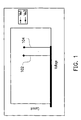
- FIG. 3 is a simplified schematic diagram of a memory array having dual function memory cells.
- Memory cells 108a through 108n are illustrated in the matrix defined by word lines (WLn) WLn-1 to WLn+1 and bit lines BLn-1 to BLn+1. Since the chalcogenide memory cells function as both a memory cell and steering device, there is no need for access transistors.
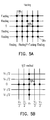
- Figures 4A through 4D illustrate exemplary plots associated with programming techniques that may be applied to a chalcogenide device.
- Figure 4A illustrates a floating programming technique.
- the chalcogenide memory device includes two voltage thresholds, i.e., a low voltage threshold (V thl ) as state 1 and a high voltage threshold (V thh ) state 0.
- the plot of Figure 4A illustrates the bias applied and the resulting bias on the cells.
- the unselected cells are associated with a bias of -V p to +V p .
- the selected cell is associated with a forward bias of +V p .
- Cell 108s represents the selected cell, while the remainder of cells 108a - 108n represent the unselected cells.
- Table 1 summarizes the programming method for program 1 and program 0.
- Program 1 Program 0 Selected Bit line 0 0 Other Bit line Floating Floating Selected Word line V pl V ph Other Word line Floating Floating As summarized in Table 1, the selected bit line is zero, while the selected word line is dependent upon the program or state selected, i.e., V pl or V ph .
- Figure 4B illustrates a biased programming technique.
- the plot of Figure 4B illustrates the bias applied.
- a voltage bias
- the selected cell 108s is associated with a forward bias of +V p .
- the chalcogenide memory device includes two voltage thresholds, i.e., a low voltage threshold (V thl ) as state 1 and a high voltage threshold (V thh ) state 0.
- V thl low voltage threshold
- V thh high voltage threshold
- Program 1 Program 0 Selected Bit line 0 0 Other Bit line 0 ⁇ V ⁇ V pl 0 ⁇ V ⁇ V ph Selected Word line V pl V ph Other Word line 0 ⁇ V ⁇ V pl 0 ⁇ V ⁇ V ph As summarized in Table 2, the selected bit line is zero, while the selected word line is dependent upon the program or state selected, i.e., V pl or V ph . It should be appreciated that two exemplary types of bias programming methods may be used, i.e., the V/2 method and the V/3 method, illustrated in Figures 4C and 4D, respectively. Of course, other bias programming methods may be used as the methods illustrated herein are exemplary and not meant to be limiting.
- Figure 4C illustrates a plot of the V/2 method.
- the plot of Figure 4C illustrates the bias applied and the resulting bias on the cell.
- the selected cell 108s is associated with a forward bias of +V p while the remaining unselected cells are associated with a forward bias of +V p /2.
- the chalcogenide memory device includes two voltage thresholds, i.e., a low voltage threshold (V thl ) as state 1 and a high voltage threshold (V thh ) state 0.
- V thl low voltage threshold
- V thh high voltage threshold
- Program 1 Program 0 Selected Bit line 0 0 Other Bit line V pl /2 V ph /2 Selected Word line V pl V ph Other Word line V pl /2 V ph /2
- the selected bit line is zero, while the selected word line is dependent upon the program or state selected, i.e., V pl or V ph .
- Figure 4D illustrates a plot of the V/3 method.
- the plot of Figure 4D illustrates the bias applied and the resulting bias on the cell.
- the selected cell 108s is associated with a forward bias of +V p while the remaining unselected cells fall into one of two characterizations, i.e., those associated with a forward bias and those associated with a reverse bias.
- Cells 108f are associated with a forward bias of +V p /3
- cells 108r are associated with a reverse bias of -V p /3.
- the chalcogenide memory device includes two voltage thresholds, i.e., a low voltage threshold (V thl ) as state 1 and a high voltage threshold (V thh ) state 0.
- the reading methods include a floating method and a bias method.
- the floating method refers to a bias V r that is applied between V thl and V thh on the selected word line (or bit line) and zero bias on the selected word line (or bit line).
- Other word lines and bit lines are floating.
- the bias method refers to a bias V r that is applied between V thl and V thh on the selected word line (or bit line) and zero bias on the selected word line (or bit line).
- Other word lines and bit lines apply a certain bias of 0 ⁇ V ⁇ V thl . Two illustrative bias methods, V/2 method and V/3 method were presented.
- Figures 5A through 5C illustrate three exemplary methods for reading a device.
- Each of Figures 5A-5C represents the bias applied and the resulting bias on the cells.
- Figure 5A represents a floating method where the bias is -V r -> +V r and selected cell 108s is associated with a forward bias of+V r .
- Figure 5B represents a V/2 reading method.
- Selected cell 108s is associated with a forward bias of +V r .
- the remaining unselected cells of Figure 5B are associated with a forward bias of +V r /2.
- Figure 5C represents a V/3 reading method.
- Selected cell 108s is associated with a forward bias of +V r .
- the remaining unselected cells of Figure 5C are associated with either a forward bias of +V r /3 or a reverse bias of -V r /3. It should be appreciated that the unselected cells form a similar pattern as discussed above with reference to Figure 4D.
- the present invention provides a memory core that eliminates the need for access transistors providing access to the core cells. That is, the access to the core cells may be accomplished through the programming of the core cells when the core cells incorporate a threshold changing material, e.g., a chalcogenide material. In essence, the steering element is now accomplished through the programming of the threshold changing material.
- a threshold changing material e.g., a chalcogenide material.
- the steering element is now accomplished through the programming of the threshold changing material.
- the elimination of the access transistors also provides for simplified decode logic as signals for the access transistors are no longer necessary for the embodiments described herein.
Landscapes
- Chemical & Material Sciences (AREA)
- Crystallography & Structural Chemistry (AREA)
- Semiconductor Memories (AREA)
- Read Only Memory (AREA)
- Non-Volatile Memory (AREA)
Applications Claiming Priority (2)
| Application Number | Priority Date | Filing Date | Title |
|---|---|---|---|
| US464938 | 2003-06-18 | ||
| US10/464,938 US7236394B2 (en) | 2003-06-18 | 2003-06-18 | Transistor-free random access memory |
Publications (2)
| Publication Number | Publication Date |
|---|---|
| EP1489621A1 true EP1489621A1 (fr) | 2004-12-22 |
| EP1489621B1 EP1489621B1 (fr) | 2007-01-17 |
Family
ID=33418163
Family Applications (1)
| Application Number | Title | Priority Date | Filing Date |
|---|---|---|---|
| EP03026609A Expired - Lifetime EP1489621B1 (fr) | 2003-06-18 | 2003-11-19 | Mémoire à accès aléatoire sans transistors |
Country Status (6)
| Country | Link |
|---|---|
| US (1) | US7236394B2 (fr) |
| EP (1) | EP1489621B1 (fr) |
| JP (1) | JP4932140B2 (fr) |
| CN (1) | CN100463074C (fr) |
| DE (1) | DE60311238T2 (fr) |
| TW (1) | TWI227056B (fr) |
Cited By (4)
| Publication number | Priority date | Publication date | Assignee | Title |
|---|---|---|---|---|
| EP2119011A4 (fr) * | 2007-03-02 | 2010-03-17 | Freescale Semiconductor Inc | Réseau de fusibles de circuit intégré |
| EP3048612A3 (fr) * | 2015-01-22 | 2016-08-24 | Nantero, Inc. | Procédés de lecture et de programmation de matrices 1-r d'éléments à changement résistif |
| US10290349B2 (en) | 2015-07-29 | 2019-05-14 | Nantero, Inc. | DDR compatible open array architectures for resistive change element arrays |
| US10340005B2 (en) | 2015-07-29 | 2019-07-02 | Nantero, Inc. | Resistive change element arrays with in situ initialization |
Families Citing this family (33)
| Publication number | Priority date | Publication date | Assignee | Title |
|---|---|---|---|---|
| US7323707B2 (en) * | 2004-06-30 | 2008-01-29 | Intel Corporation | Initializing phase change memories |
| US7646630B2 (en) * | 2004-11-08 | 2010-01-12 | Ovonyx, Inc. | Programmable matrix array with chalcogenide material |
| US7626859B2 (en) * | 2006-02-16 | 2009-12-01 | Samsung Electronics Co., Ltd. | Phase-change random access memory and programming method |
| KR100849717B1 (ko) * | 2006-12-28 | 2008-08-01 | 주식회사 하이닉스반도체 | 문턱전압 스위칭소자를 구비하는 메모리장치 |
| JP5539610B2 (ja) * | 2007-03-02 | 2014-07-02 | ピーエスフォー ルクスコ エスエイアールエル | 相変化メモリのプログラム方法と読み出し方法 |
| US7787323B2 (en) | 2007-04-27 | 2010-08-31 | Freescale Semiconductor, Inc. | Level detect circuit |
| US7663900B2 (en) * | 2007-12-31 | 2010-02-16 | Hitachi Global Storage Technologies Netherlands B.V. | Tree-structure memory device |
| US7936597B2 (en) * | 2008-03-25 | 2011-05-03 | Seagate Technology Llc | Multilevel magnetic storage device |
| US7974119B2 (en) | 2008-07-10 | 2011-07-05 | Seagate Technology Llc | Transmission gate-based spin-transfer torque memory unit |
| US20100090189A1 (en) * | 2008-09-15 | 2010-04-15 | Savransky Semyon D | Nanoscale electrical device |
| US9030867B2 (en) * | 2008-10-20 | 2015-05-12 | Seagate Technology Llc | Bipolar CMOS select device for resistive sense memory |
| US7936580B2 (en) | 2008-10-20 | 2011-05-03 | Seagate Technology Llc | MRAM diode array and access method |
| US7974117B2 (en) * | 2008-10-30 | 2011-07-05 | Seagate Technology Llc | Non-volatile memory cell with programmable unipolar switching element |
| US7936583B2 (en) * | 2008-10-30 | 2011-05-03 | Seagate Technology Llc | Variable resistive memory punchthrough access method |
| US7825478B2 (en) * | 2008-11-07 | 2010-11-02 | Seagate Technology Llc | Polarity dependent switch for resistive sense memory |
| US8178864B2 (en) | 2008-11-18 | 2012-05-15 | Seagate Technology Llc | Asymmetric barrier diode |
| US8203869B2 (en) | 2008-12-02 | 2012-06-19 | Seagate Technology Llc | Bit line charge accumulation sensing for resistive changing memory |
| US8159856B2 (en) | 2009-07-07 | 2012-04-17 | Seagate Technology Llc | Bipolar select device for resistive sense memory |
| US8158964B2 (en) | 2009-07-13 | 2012-04-17 | Seagate Technology Llc | Schottky diode switch and memory units containing the same |
| US8248836B2 (en) * | 2009-07-13 | 2012-08-21 | Seagate Technology Llc | Non-volatile memory cell stack with dual resistive elements |
| US7936585B2 (en) * | 2009-07-13 | 2011-05-03 | Seagate Technology Llc | Non-volatile memory cell with non-ohmic selection layer |
| US8648426B2 (en) | 2010-12-17 | 2014-02-11 | Seagate Technology Llc | Tunneling transistors |
| US8605495B2 (en) | 2011-05-09 | 2013-12-10 | Macronix International Co., Ltd. | Isolation device free memory |
| US9117515B2 (en) | 2012-01-18 | 2015-08-25 | Macronix International Co., Ltd. | Programmable metallization cell with two dielectric layers |
| JP2013200929A (ja) | 2012-03-26 | 2013-10-03 | Toshiba Corp | 半導体記憶装置 |
| US9437266B2 (en) | 2012-11-13 | 2016-09-06 | Macronix International Co., Ltd. | Unipolar programmable metallization cell |
| US9379126B2 (en) | 2013-03-14 | 2016-06-28 | Macronix International Co., Ltd. | Damascene conductor for a 3D device |
| US9099538B2 (en) | 2013-09-17 | 2015-08-04 | Macronix International Co., Ltd. | Conductor with a plurality of vertical extensions for a 3D device |
| US9559113B2 (en) | 2014-05-01 | 2017-01-31 | Macronix International Co., Ltd. | SSL/GSL gate oxide in 3D vertical channel NAND |
| GB2545264B (en) * | 2015-12-11 | 2020-01-15 | Advanced Risc Mach Ltd | A storage array |
| US9793323B1 (en) | 2016-07-11 | 2017-10-17 | Macronix International Co., Ltd. | Phase change memory with high endurance |
| US10510957B2 (en) * | 2017-07-26 | 2019-12-17 | Micron Technology, Inc. | Self-aligned memory decks in cross-point memory arrays |
| US10381075B2 (en) * | 2017-12-14 | 2019-08-13 | Micron Technology, Inc. | Techniques to access a self-selecting memory device |
Citations (4)
| Publication number | Priority date | Publication date | Assignee | Title |
|---|---|---|---|---|
| US3530441A (en) * | 1969-01-15 | 1970-09-22 | Energy Conversion Devices Inc | Method and apparatus for storing and retrieving information |
| US4199692A (en) * | 1978-05-16 | 1980-04-22 | Harris Corporation | Amorphous non-volatile ram |
| US20030081451A1 (en) * | 2001-10-30 | 2003-05-01 | Lowrey Tyler A. | Technique and apparatus for performing write operations to a phase change material memory device |
| WO2003079463A2 (fr) * | 2002-03-15 | 2003-09-25 | Axon Technologies Corporation | Structure programmable, reseau comprenant cette structure et procedes de production de celle-ci |
Family Cites Families (15)
| Publication number | Priority date | Publication date | Assignee | Title |
|---|---|---|---|---|
| US5761115A (en) * | 1996-05-30 | 1998-06-02 | Axon Technologies Corporation | Programmable metallization cell structure and method of making same |
| US5952671A (en) * | 1997-05-09 | 1999-09-14 | Micron Technology, Inc. | Small electrode for a chalcogenide switching device and method for fabricating same |
| JPH1197556A (ja) * | 1997-09-18 | 1999-04-09 | Seiko Epson Corp | 薄膜半導体装置及びicカード、これらの製造方法及び書込み読出し方法並びに電子機器 |
| JP3404330B2 (ja) * | 1999-08-02 | 2003-05-06 | 株式会社日立製作所 | 半導体装置及びその駆動方法 |
| JP4491870B2 (ja) * | 1999-10-27 | 2010-06-30 | ソニー株式会社 | 不揮発性メモリの駆動方法 |
| US6205056B1 (en) * | 2000-03-14 | 2001-03-20 | Advanced Micro Devices, Inc. | Automated reference cell trimming verify |
| US6631085B2 (en) * | 2000-04-28 | 2003-10-07 | Matrix Semiconductor, Inc. | Three-dimensional memory array incorporating serial chain diode stack |
| NO312699B1 (no) * | 2000-07-07 | 2002-06-17 | Thin Film Electronics Asa | Adressering av minnematrise |
| US6449190B1 (en) * | 2001-01-17 | 2002-09-10 | Advanced Micro Devices, Inc. | Adaptive reference cells for a memory device |
| US6545898B1 (en) * | 2001-03-21 | 2003-04-08 | Silicon Valley Bank | Method and apparatus for writing memory arrays using external source of high programming voltage |
| US6490203B1 (en) * | 2001-05-24 | 2002-12-03 | Edn Silicon Devices, Inc. | Sensing scheme of flash EEPROM |
| JP4169249B2 (ja) * | 2001-11-15 | 2008-10-22 | 大日本印刷株式会社 | 相変化型メモリ素子の製造方法および該方法で製造したメモリ素子 |
| TWI233204B (en) * | 2002-07-26 | 2005-05-21 | Infineon Technologies Ag | Nonvolatile memory element and associated production methods and memory element arrangements |
| US6795338B2 (en) * | 2002-12-13 | 2004-09-21 | Intel Corporation | Memory having access devices using phase change material such as chalcogenide |
| US6735114B1 (en) * | 2003-02-04 | 2004-05-11 | Advanced Micro Devices, Inc. | Method of improving dynamic reference tracking for flash memory unit |
-
2003
- 2003-06-18 US US10/464,938 patent/US7236394B2/en not_active Expired - Lifetime
- 2003-10-30 TW TW092130180A patent/TWI227056B/zh not_active IP Right Cessation
- 2003-11-19 DE DE60311238T patent/DE60311238T2/de not_active Expired - Lifetime
- 2003-11-19 EP EP03026609A patent/EP1489621B1/fr not_active Expired - Lifetime
- 2003-11-24 CN CNB2003101152427A patent/CN100463074C/zh not_active Expired - Lifetime
-
2004
- 2004-05-18 JP JP2004148081A patent/JP4932140B2/ja not_active Expired - Lifetime
Patent Citations (4)
| Publication number | Priority date | Publication date | Assignee | Title |
|---|---|---|---|---|
| US3530441A (en) * | 1969-01-15 | 1970-09-22 | Energy Conversion Devices Inc | Method and apparatus for storing and retrieving information |
| US4199692A (en) * | 1978-05-16 | 1980-04-22 | Harris Corporation | Amorphous non-volatile ram |
| US20030081451A1 (en) * | 2001-10-30 | 2003-05-01 | Lowrey Tyler A. | Technique and apparatus for performing write operations to a phase change material memory device |
| WO2003079463A2 (fr) * | 2002-03-15 | 2003-09-25 | Axon Technologies Corporation | Structure programmable, reseau comprenant cette structure et procedes de production de celle-ci |
Non-Patent Citations (1)
| Title |
|---|
| STEVENTON A G: "The switching mechanisms in amorphous chalcogenide memory devices", JOURNAL OF NON-CRYSTALLINE SOLIDS, AUG. 1976, NETHERLANDS, vol. 21, no. 3, pages 319 - 329, XP002278873, ISSN: 0022-3093 * |
Cited By (5)
| Publication number | Priority date | Publication date | Assignee | Title |
|---|---|---|---|---|
| EP2119011A4 (fr) * | 2007-03-02 | 2010-03-17 | Freescale Semiconductor Inc | Réseau de fusibles de circuit intégré |
| EP3048612A3 (fr) * | 2015-01-22 | 2016-08-24 | Nantero, Inc. | Procédés de lecture et de programmation de matrices 1-r d'éléments à changement résistif |
| US9715927B2 (en) | 2015-01-22 | 2017-07-25 | Nantero, Inc. | 1-R resistive change element arrays using resistive reference elements |
| US10290349B2 (en) | 2015-07-29 | 2019-05-14 | Nantero, Inc. | DDR compatible open array architectures for resistive change element arrays |
| US10340005B2 (en) | 2015-07-29 | 2019-07-02 | Nantero, Inc. | Resistive change element arrays with in situ initialization |
Also Published As
| Publication number | Publication date |
|---|---|
| TW200501402A (en) | 2005-01-01 |
| CN100463074C (zh) | 2009-02-18 |
| JP2005011495A (ja) | 2005-01-13 |
| JP4932140B2 (ja) | 2012-05-16 |
| CN1574067A (zh) | 2005-02-02 |
| DE60311238D1 (de) | 2007-03-08 |
| DE60311238T2 (de) | 2007-05-16 |
| TWI227056B (en) | 2005-01-21 |
| US7236394B2 (en) | 2007-06-26 |
| US20040257872A1 (en) | 2004-12-23 |
| EP1489621B1 (fr) | 2007-01-17 |
Similar Documents
| Publication | Publication Date | Title |
|---|---|---|
| US7236394B2 (en) | Transistor-free random access memory | |
| US6865117B2 (en) | Programming circuit for a programmable microelectronic device, system including the circuit, and method of forming the same | |
| US7248507B2 (en) | CMIS semiconductor nonvolatile storage circuit | |
| KR100692278B1 (ko) | 비휘발성 반도체메모리장치 | |
| JP3167919B2 (ja) | Nand構造の不揮発性半導体メモリとそのプログラム方法 | |
| JP3913906B2 (ja) | 強誘電体ランダムアクセスメモリ装置 | |
| US7180767B2 (en) | Multi-level memory device and methods for programming and reading the same | |
| US4617652A (en) | Integrated high voltage distribution and control systems | |
| US6628544B2 (en) | Flash memory cell and method to achieve multiple bits per cell | |
| US20050270886A1 (en) | Ferroelectric memory device and read control method thereof | |
| US7215567B2 (en) | Ferroelectric memory device | |
| EP2439746B1 (fr) | Mémoire non volatile unique en silicium | |
| WO2011049628A1 (fr) | Nouveau schéma de programme sans perçage pour conception de mémoire flash à chaîne nt | |
| US10255953B2 (en) | Bi-directional RRAM decoder-driver | |
| US9530495B1 (en) | Resistive switching memory having a resistor, diode, and switch memory cell | |
| KR20010075543A (ko) | 반도체 장치 | |
| CN101989454A (zh) | 半导体存储器件及其操作方法 | |
| JP2014053374A (ja) | 半導体集積回路 | |
| US20050041467A1 (en) | Chalcogenide memory | |
| US9887003B2 (en) | Semiconductor storage device | |
| US11735266B2 (en) | Antifuse-type one time programming memory cell and cell array structure with same | |
| US12069873B2 (en) | Resistive memory cell and associated cell array structure | |
| WO2003058638A1 (fr) | Circuit de programmation pour dispositif micro-electronique programmable, systeme incluant le circuit et procede de fabrication de ce circuit | |
| US6396095B1 (en) | Semiconductor memory and method of driving semiconductor memory | |
| US6128221A (en) | Circuit and programming method for the operation of flash memories to prevent programming disturbances |
Legal Events
| Date | Code | Title | Description |
|---|---|---|---|
| PUAI | Public reference made under article 153(3) epc to a published international application that has entered the european phase |
Free format text: ORIGINAL CODE: 0009012 |
|
| 17P | Request for examination filed |
Effective date: 20031119 |
|
| AK | Designated contracting states |
Kind code of ref document: A1 Designated state(s): AT BE BG CH CY CZ DE DK EE ES FI FR GB GR HU IE IT LI LU MC NL PT RO SE SI SK TR |
|
| AX | Request for extension of the european patent |
Extension state: AL LT LV MK |
|
| 17Q | First examination report despatched |
Effective date: 20050224 |
|
| AKX | Designation fees paid |
Designated state(s): DE FR GB IT |
|
| GRAP | Despatch of communication of intention to grant a patent |
Free format text: ORIGINAL CODE: EPIDOSNIGR1 |
|
| GRAS | Grant fee paid |
Free format text: ORIGINAL CODE: EPIDOSNIGR3 |
|
| GRAA | (expected) grant |
Free format text: ORIGINAL CODE: 0009210 |
|
| AK | Designated contracting states |
Kind code of ref document: B1 Designated state(s): DE FR GB IT |
|
| REG | Reference to a national code |
Ref country code: GB Ref legal event code: FG4D |
|
| REF | Corresponds to: |
Ref document number: 60311238 Country of ref document: DE Date of ref document: 20070308 Kind code of ref document: P |
|
| ET | Fr: translation filed | ||
| PLBE | No opposition filed within time limit |
Free format text: ORIGINAL CODE: 0009261 |
|
| STAA | Information on the status of an ep patent application or granted ep patent |
Free format text: STATUS: NO OPPOSITION FILED WITHIN TIME LIMIT |
|
| 26N | No opposition filed |
Effective date: 20071018 |
|
| REG | Reference to a national code |
Ref country code: FR Ref legal event code: PLFP Year of fee payment: 13 |
|
| REG | Reference to a national code |
Ref country code: FR Ref legal event code: PLFP Year of fee payment: 14 |
|
| REG | Reference to a national code |
Ref country code: FR Ref legal event code: PLFP Year of fee payment: 15 |
|
| REG | Reference to a national code |
Ref country code: FR Ref legal event code: PLFP Year of fee payment: 16 |
|
| PGFP | Annual fee paid to national office [announced via postgrant information from national office to epo] |
Ref country code: IT Payment date: 20220831 Year of fee payment: 20 Ref country code: GB Payment date: 20220907 Year of fee payment: 20 |
|
| PGFP | Annual fee paid to national office [announced via postgrant information from national office to epo] |
Ref country code: FR Payment date: 20220907 Year of fee payment: 20 |
|
| PGFP | Annual fee paid to national office [announced via postgrant information from national office to epo] |
Ref country code: DE Payment date: 20220908 Year of fee payment: 20 |
|
| REG | Reference to a national code |
Ref country code: DE Ref legal event code: R071 Ref document number: 60311238 Country of ref document: DE |
|
| REG | Reference to a national code |
Ref country code: GB Ref legal event code: PE20 Expiry date: 20231118 |
|
| PG25 | Lapsed in a contracting state [announced via postgrant information from national office to epo] |
Ref country code: GB Free format text: LAPSE BECAUSE OF EXPIRATION OF PROTECTION Effective date: 20231118 |
|
| PG25 | Lapsed in a contracting state [announced via postgrant information from national office to epo] |
Ref country code: GB Free format text: LAPSE BECAUSE OF EXPIRATION OF PROTECTION Effective date: 20231118 |