EP1490877B1 - Couche de detection ferrimagnetique synthetique pour applications magnetiques a acces aleatoire (mram) - Google Patents
Couche de detection ferrimagnetique synthetique pour applications magnetiques a acces aleatoire (mram) Download PDFInfo
- Publication number
- EP1490877B1 EP1490877B1 EP03746039A EP03746039A EP1490877B1 EP 1490877 B1 EP1490877 B1 EP 1490877B1 EP 03746039 A EP03746039 A EP 03746039A EP 03746039 A EP03746039 A EP 03746039A EP 1490877 B1 EP1490877 B1 EP 1490877B1
- Authority
- EP
- European Patent Office
- Prior art keywords
- layer
- layers
- ferromagnetic
- magnetizable
- sense
- Prior art date
- Legal status (The legal status is an assumption and is not a legal conclusion. Google has not performed a legal analysis and makes no representation as to the accuracy of the status listed.)
- Expired - Lifetime
Links
- 230000005291 magnetic effect Effects 0.000 claims abstract description 119
- 125000006850 spacer group Chemical group 0.000 claims abstract description 57
- 230000008878 coupling Effects 0.000 claims abstract description 54
- 238000010168 coupling process Methods 0.000 claims abstract description 54
- 238000005859 coupling reaction Methods 0.000 claims abstract description 54
- 239000000463 material Substances 0.000 claims abstract description 40
- 230000005316 antiferromagnetic exchange Effects 0.000 claims abstract description 23
- 230000004888 barrier function Effects 0.000 claims abstract description 8
- 230000005294 ferromagnetic effect Effects 0.000 claims description 80
- 230000005415 magnetization Effects 0.000 claims description 36
- 238000000034 method Methods 0.000 claims description 26
- 230000005290 antiferromagnetic effect Effects 0.000 claims description 22
- 239000004020 conductor Substances 0.000 claims description 16
- 229910001030 Iron–nickel alloy Inorganic materials 0.000 claims description 12
- 238000004519 manufacturing process Methods 0.000 claims description 4
- 229910052742 iron Inorganic materials 0.000 claims description 2
- 229910052759 nickel Inorganic materials 0.000 claims description 2
- 239000000758 substrate Substances 0.000 claims description 2
- 229910003321 CoFe Inorganic materials 0.000 claims 6
- 238000009499 grossing Methods 0.000 claims 2
- 230000005641 tunneling Effects 0.000 abstract description 2
- 239000010410 layer Substances 0.000 description 227
- 101150081099 OGA gene Proteins 0.000 description 24
- 230000005293 ferrimagnetic effect Effects 0.000 description 20
- 230000003993 interaction Effects 0.000 description 20
- 230000000694 effects Effects 0.000 description 12
- 239000003302 ferromagnetic material Substances 0.000 description 11
- 230000007423 decrease Effects 0.000 description 9
- 229910052751 metal Inorganic materials 0.000 description 8
- 239000002184 metal Substances 0.000 description 8
- 238000012545 processing Methods 0.000 description 8
- 238000013461 design Methods 0.000 description 7
- 239000002356 single layer Substances 0.000 description 6
- 229910052802 copper Inorganic materials 0.000 description 5
- 239000010949 copper Substances 0.000 description 5
- 229910045601 alloy Inorganic materials 0.000 description 4
- 239000000956 alloy Substances 0.000 description 4
- PNEYBMLMFCGWSK-UHFFFAOYSA-N aluminium oxide Inorganic materials [O-2].[O-2].[O-2].[Al+3].[Al+3] PNEYBMLMFCGWSK-UHFFFAOYSA-N 0.000 description 4
- 230000008901 benefit Effects 0.000 description 4
- 230000001419 dependent effect Effects 0.000 description 4
- 230000006870 function Effects 0.000 description 4
- AMWRITDGCCNYAT-UHFFFAOYSA-L hydroxy(oxo)manganese;manganese Chemical compound [Mn].O[Mn]=O.O[Mn]=O AMWRITDGCCNYAT-UHFFFAOYSA-L 0.000 description 4
- 239000002885 antiferromagnetic material Substances 0.000 description 3
- 238000003491 array Methods 0.000 description 3
- 230000008859 change Effects 0.000 description 3
- 238000005516 engineering process Methods 0.000 description 3
- 150000002500 ions Chemical group 0.000 description 3
- 230000005389 magnetism Effects 0.000 description 3
- RYGMFSIKBFXOCR-UHFFFAOYSA-N Copper Chemical compound [Cu] RYGMFSIKBFXOCR-UHFFFAOYSA-N 0.000 description 2
- 229910015136 FeMn Inorganic materials 0.000 description 2
- 229910003289 NiMn Inorganic materials 0.000 description 2
- 229910019041 PtMn Inorganic materials 0.000 description 2
- 230000006399 behavior Effects 0.000 description 2
- 238000004364 calculation method Methods 0.000 description 2
- 230000014759 maintenance of location Effects 0.000 description 2
- 230000007246 mechanism Effects 0.000 description 2
- 150000002739 metals Chemical class 0.000 description 2
- 230000005298 paramagnetic effect Effects 0.000 description 2
- 230000004044 response Effects 0.000 description 2
- 229910052707 ruthenium Inorganic materials 0.000 description 2
- 238000000926 separation method Methods 0.000 description 2
- 239000007787 solid Substances 0.000 description 2
- 230000002269 spontaneous effect Effects 0.000 description 2
- 238000003860 storage Methods 0.000 description 2
- -1 IrMn Inorganic materials 0.000 description 1
- 230000005303 antiferromagnetism Effects 0.000 description 1
- 238000013459 approach Methods 0.000 description 1
- 150000001875 compounds Chemical class 0.000 description 1
- 239000002772 conduction electron Substances 0.000 description 1
- 239000011529 conductive interlayer Substances 0.000 description 1
- 238000010276 construction Methods 0.000 description 1
- 229910052593 corundum Inorganic materials 0.000 description 1
- 230000003247 decreasing effect Effects 0.000 description 1
- 238000005530 etching Methods 0.000 description 1
- 230000002349 favourable effect Effects 0.000 description 1
- 239000002902 ferrimagnetic material Substances 0.000 description 1
- 230000004907 flux Effects 0.000 description 1
- 239000011810 insulating material Substances 0.000 description 1
- 239000012212 insulator Substances 0.000 description 1
- 239000011229 interlayer Substances 0.000 description 1
- 229910000765 intermetallic Inorganic materials 0.000 description 1
- 230000005381 magnetic domain Effects 0.000 description 1
- 239000000696 magnetic material Substances 0.000 description 1
- 229910001437 manganese ion Inorganic materials 0.000 description 1
- 230000001404 mediated effect Effects 0.000 description 1
- GNRSAWUEBMWBQH-UHFFFAOYSA-N nickel(II) oxide Inorganic materials [Ni]=O GNRSAWUEBMWBQH-UHFFFAOYSA-N 0.000 description 1
- 238000005457 optimization Methods 0.000 description 1
- 230000010355 oscillation Effects 0.000 description 1
- 239000002907 paramagnetic material Substances 0.000 description 1
- 230000008569 process Effects 0.000 description 1
- 230000009467 reduction Effects 0.000 description 1
- 239000004065 semiconductor Substances 0.000 description 1
- 238000004088 simulation Methods 0.000 description 1
- 238000004544 sputter deposition Methods 0.000 description 1
- 239000000126 substance Substances 0.000 description 1
- 238000012546 transfer Methods 0.000 description 1
- 229910052723 transition metal Inorganic materials 0.000 description 1
- 150000003624 transition metals Chemical class 0.000 description 1
- 229910001845 yogo sapphire Inorganic materials 0.000 description 1
- 229910000859 α-Fe Inorganic materials 0.000 description 1
Images



Classifications
-
- B—PERFORMING OPERATIONS; TRANSPORTING
- B82—NANOTECHNOLOGY
- B82Y—SPECIFIC USES OR APPLICATIONS OF NANOSTRUCTURES; MEASUREMENT OR ANALYSIS OF NANOSTRUCTURES; MANUFACTURE OR TREATMENT OF NANOSTRUCTURES
- B82Y25/00—Nanomagnetism, e.g. magnetoimpedance, anisotropic magnetoresistance, giant magnetoresistance or tunneling magnetoresistance
-
- G—PHYSICS
- G11—INFORMATION STORAGE
- G11C—STATIC STORES
- G11C11/00—Digital stores characterised by the use of particular electric or magnetic storage elements; Storage elements therefor
-
- G—PHYSICS
- G11—INFORMATION STORAGE
- G11C—STATIC STORES
- G11C11/00—Digital stores characterised by the use of particular electric or magnetic storage elements; Storage elements therefor
- G11C11/02—Digital stores characterised by the use of particular electric or magnetic storage elements; Storage elements therefor using magnetic elements
- G11C11/14—Digital stores characterised by the use of particular electric or magnetic storage elements; Storage elements therefor using magnetic elements using thin-film elements
- G11C11/15—Digital stores characterised by the use of particular electric or magnetic storage elements; Storage elements therefor using magnetic elements using thin-film elements using multiple magnetic layers
-
- G—PHYSICS
- G11—INFORMATION STORAGE
- G11C—STATIC STORES
- G11C11/00—Digital stores characterised by the use of particular electric or magnetic storage elements; Storage elements therefor
- G11C11/02—Digital stores characterised by the use of particular electric or magnetic storage elements; Storage elements therefor using magnetic elements
- G11C11/16—Digital stores characterised by the use of particular electric or magnetic storage elements; Storage elements therefor using magnetic elements using elements in which the storage effect is based on magnetic spin effect
-
- G—PHYSICS
- G11—INFORMATION STORAGE
- G11C—STATIC STORES
- G11C11/00—Digital stores characterised by the use of particular electric or magnetic storage elements; Storage elements therefor
- G11C11/02—Digital stores characterised by the use of particular electric or magnetic storage elements; Storage elements therefor using magnetic elements
- G11C11/16—Digital stores characterised by the use of particular electric or magnetic storage elements; Storage elements therefor using magnetic elements using elements in which the storage effect is based on magnetic spin effect
- G11C11/161—Digital stores characterised by the use of particular electric or magnetic storage elements; Storage elements therefor using magnetic elements using elements in which the storage effect is based on magnetic spin effect details concerning the memory cell structure, e.g. the layers of the ferromagnetic memory cell
-
- G—PHYSICS
- G11—INFORMATION STORAGE
- G11C—STATIC STORES
- G11C11/00—Digital stores characterised by the use of particular electric or magnetic storage elements; Storage elements therefor
- G11C11/02—Digital stores characterised by the use of particular electric or magnetic storage elements; Storage elements therefor using magnetic elements
- G11C11/16—Digital stores characterised by the use of particular electric or magnetic storage elements; Storage elements therefor using magnetic elements using elements in which the storage effect is based on magnetic spin effect
- G11C11/165—Auxiliary circuits
- G11C11/1659—Cell access
-
- G—PHYSICS
- G11—INFORMATION STORAGE
- G11C—STATIC STORES
- G11C11/00—Digital stores characterised by the use of particular electric or magnetic storage elements; Storage elements therefor
- G11C11/02—Digital stores characterised by the use of particular electric or magnetic storage elements; Storage elements therefor using magnetic elements
- G11C11/16—Digital stores characterised by the use of particular electric or magnetic storage elements; Storage elements therefor using magnetic elements using elements in which the storage effect is based on magnetic spin effect
- G11C11/165—Auxiliary circuits
- G11C11/1673—Reading or sensing circuits or methods
-
- H—ELECTRICITY
- H01—ELECTRIC ELEMENTS
- H01F—MAGNETS; INDUCTANCES; TRANSFORMERS; SELECTION OF MATERIALS FOR THEIR MAGNETIC PROPERTIES
- H01F10/00—Thin magnetic films, e.g. of one-domain structure
- H01F10/32—Spin-exchange-coupled multilayers, e.g. nanostructured superlattices
-
- H—ELECTRICITY
- H01—ELECTRIC ELEMENTS
- H01F—MAGNETS; INDUCTANCES; TRANSFORMERS; SELECTION OF MATERIALS FOR THEIR MAGNETIC PROPERTIES
- H01F10/00—Thin magnetic films, e.g. of one-domain structure
- H01F10/32—Spin-exchange-coupled multilayers, e.g. nanostructured superlattices
- H01F10/3218—Exchange coupling of magnetic films via an antiferromagnetic interface
Definitions
- This invention relates generally to the field of nonvolatile memory devices for use as computer storage, and in particular to nonvolatile memory arrays that use magnetic memory elements as the individual data bits.
- MRAM Magnetic Random Access Memory
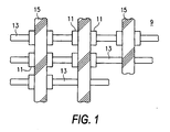
- An MRAM device typically includes an array of magnetic memory elements 11 located at the intersections of row line 13 and column line 15 conductors as illustrated in Figure 1 .
- a simple magnetic memory element has a structure which is shown in more detail in Figure 2 .
- the magnetic memory element includes ferromagnetic layers 17 and 19 separated by a nonmagnetic layer 21.
- the magnetization in one ferromagnetic layer 17, typically referred to as the pinned layer is fixed in one direction.
- the magnetization of the other ferromagnetic layer 19, often referred to as the sense layer is not pinned, so its magnetization is free to switch between "parallel” and "anti-parallel” states relative to the magnetization of the pinned layer.
- the sense layer may also be referred to as the "free” layer or storage layer, thus it should be understood that when the term “sense layer” is used, the meaning of this term should not be limited to this terminology but rather the function the layer performs.
- the logical value or bit stored in an MRAM memory element is associated with a resistance value, and the resistance of the memory element is determined by the relative orientation of the sense layer magnetization with respect to the pinned layer magnetization orientation. A parallel orientation of the magnetization of the sense layer with respect to the pinned layer magnetization results in a low resistance. Conversely, in response to the anti-parallel orientation, the magnetic memory element will show a high resistance. Referring to Figure 2 , the manner in which the resistance of the memory element is read is dependent on the type of material used to form the nonmagnetic spacer layer 21 separating the pinned layer 17 from the sense layer 19.
- the resistance value of the memory element can be sensed via the giant magnetoresistance effect, which usually involves running a current parallel to the long axis 20 of the memory element. If the nonmagnetic spacer layer is composed of an insulating material, such as alumina, then the resistance value can be sensed using the tunneling magnetoresistance effect, and this is accomplished by running a current perpendicular to the plane of the nonmagnetic spacer layer 21 from the sense layer 19 to the pinned layer 17.
- a logical "0" or “1” is usually written into the magnetic memory element by applying external magnetic fields (via an electrical current) that rotate the magnetization direction of the sense layer.
- an MRAM memory element is designed so that the magnetization of the sense layer and the pinned layer aligns along an axis known as the easy axis 27.
- External magnetic fields are applied to flip the orientation of the sense layer along its easy axis to either the parallel or anti-parallel orientation with respect to the orientation of the magnetization of the pinned layer, depending on the logic state to be stored.
- MRAM devices typically include an orthogonal array of row and column lines (electrical conductors) that are used to apply external magnetic fields to the magnetic memory elements during writing and may also be used to sense the resistance of a memory element during reading. Additional write and read conductors may also be present in the array. In the two conductor level implementation shown in figure 1 , the magnetic memory elements are located at the intersections of the row 13 and column 15 lines.
- the magnetic field that is generated by running a current through the column line 15 is referred to herein as the easy-axis write field.
- the easy-axis write field is collinear with the easy axis 23 of the MRAM bit 11 ( Fig. 2a ).
- the magnetic field that is generated when a current is run through the row conductive line 13 is referred to as the hard-axis write field.
- the hard-axis write field generated by the row conductive line 13 runs parallel to the hard axis 25 of the MRAM bit 11.
- a memory element is selected for writing when it is exposed to both a hard-axis and an easy-axis write field.
- Each write field, by itself and when generated with only one of the two conductive lines, is therefore commonly referred to as a half-select field because a single field by itself should not be of sufficient magnitude to switch the magnetization orientation of the sense layer of a memory element.
- the hard-axis write field is often referred to as the half-select field
- the easy-axis write field is often referred to as the switching field.
- These two fields are used to perform write operations on a specific memory element when applied in conjunction with each other by passing current through conductors 13, 15 ( Fig. 1 ) intersecting at the selected element.
- the bit stored at the selected memory element being accessed for a read or write operation is referred to herein as a "selected bit".
- This method for selecting a bit for writing is not ideal.
- the unselected memory elements coupled to the particular column line 15 are exposed to the easy-axis write field.
- the unselected memory elements 11 coupled to the particular row line 13 are exposed to the hard-axis write field. It is thus important to limit stray magnetic fields in the array of MRAM memory elements to a value that cannot cause half-selected bits to be written.
- Some sources of stray fields include fields from neighboring write conductors, stray fields emanating from the ferromagnetic layers of neighboring memory elements, and fields generated by sources external to the MRAM device.
- stray fields may also inhibit a selected memory element from being written, if the combined value of the stray, hard-axis, and easy-axis fields is too small for a bit to be written.
- Another source of non-ideal behavior that manifests itself in the write current required to write a memory element results from the difficulty in making an array of MRAM memory elements that respond identically to the applied write fields.
- the particular value of the hard and easy-axis write fields, and thus the row and column line write currents, is a compromise such that selected memory elements are selected with enough margin that they are always written and unselected memory elements are never exposed to a field large enough that they are unintentionally written.
- Thermal fluctuation in a seemingly unfluctuating macroscopic observable quantity such as the magnetization of a ferromagnetic material
- the orientation and magnitude of the magnetization of a ferromagnetic material are in actuality statistical quantities.
- fluctuations in thermal energy are continually occurring on a microscopic scale, where the magnitude of the thermal fluctuations is determined by the temperature T of the material. These fluctuations when averaged over the entire volume of the specimen in question determine the macroscopically observable property of the system.
- the probability for any atom in a ferromagnetic material to have a magnetic moment oriented in a particular direction is proportional to the Boltzmann factor, e -U/ KbT .
- U is the energy associated with, in this case, a particular magnetic moment orientation
- K b is Boltzman's constant.
- U sw U v V.
- U sw / K b T the orientation of the sense layer's magnetization is unstable to thermal fluctuations.
- Memory bits that are characterized by low values of U sw / K b T tend to have poor data retention times. Wait long enough and a fluctuation can spontaneously reverse the magnetization.
- a magnetic memory element that can spontaneously reverse its magnetization on a time scale short compared to the required data retention time is said to have hit the superparamagnetic limit.
- magnetic memory elements also become more susceptible to half-select write events or the occasional inability to write a selected memory element, as a thermal fluctuation may inhibit a bit from writing in a specified time interval, or it may write a half-selected bit in a specified time interval.
- increasing MRAM memory density necessitates a decrease in the volume of an MRAM bit and thus pushes the technology closer to the superparamagnetic limit or to the regime where thermal fluctuation becomes a problem.
- MRAM memory elements also suffer from inter-bit interactions resulting from stray magnetic fields that emanate from the magnetic memory element 11 sense layers.
- the sense layer of an MRAM memory element 11 produces stray fields because it is not a closed magnetic flux structure. It thus forms poles at the edges of the sense layer in response to the orientation of the sense layer magnetization. The orientation of the stray field therefore changes with the orientation of the magnetization of a sense layer in a memory element.
- the stray fields produced by these poles decrease in value with increasing distance from the sense layer.
- the stray fields from the neighboring bits may, however, be significant compared to the field required to switch the bit. In future MRAM designs, memory elements will need to be packed together more closely, which will compound this problem.
- EP-A-1182713 discloses a sense layer according to the precharacterising portion of claim 1.
- the invention provides a sense layer and a method of manufacture as defined in Claims 1 and 19.
- the present invention can minimize problems associated with increased MRAM memory density due to thermal fluctuation instability and stray field interactions, through the use of an improved sense layer.
- the stack of the modified MRAM bit 11 is constructed with a synthetic ferrimagnet as the sense layer.
- the sense layer is designed so that the synthetic ferrimagnet's ferromagnetic layers are both stray field coupled and antiferromagnetically exchange coupled via an RKKY interaction through a spacer layer composed of a metallic compound, such as Ru or Cu.
- Fig. 1 illustrates a top view of a simplified portion of an array 9 of magnetic tunnel junction memory elements 11.
- a plurality of column conductive lines 15, also called column lines, is each respectively formed over a plurality of memory elements 11 in each column of the array 9.
- a plurality of row conductive lines 13, also called a row lines, is each respectively formed beneath the memory elements 11 in each row of the array 9.
- the row lines 13 supply the hard-axis magnetic field, also known as a half-select field to the memory elements 11, while the column lines 15 supply the easy-axis switching field to the memory elements 11.
- the row 13 and column 15 lines can also be used to read magnetic memory elements 11 in addition to writing the memory elements 11.
- the array 9 can also be constructed with row line 13 above and the column line 15 below each memory element 11.
- Fig. 1 depicts one arrangement for an MRAM array, others are also possible.
- a plurality of arrays 9 of memory elements 11 may be provided in an MRAM memory device stacked one over the other.
- reading of the magnetic memory elements 11 can be accomplished using a variety of conductors as well as conductor arrangements including additional or different conductors situated above, below or in the same layer as the sense layer.
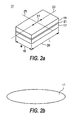
- Fig. 2a shows a perspective view of a magnetic tunnel junction memory bit 11, which is simplified for illustration purposes.
- the width (W) of the memory element 18 is defined as the distance along the hard-axis 25 of the memory element's sense layer.
- the length (L) of the memory element 20 is defined as the distance along the easy magnetic axis 23 of the memory element's sense layer.
- the length (L) dimension 20 of the memory element 11 is normally larger than the memory element's width dimension (W) 18.
- the aspect ratio of the sense layer may be defined as L/W.
- the sense layer 19 is manufactured to have a preferred axis for the two equilibrium magnetization moment orientations 27 of the sense layer 19 in the absence of an applied magnetic field (H).
- H an applied magnetic field
- the pinned layer 17 may be fabricated to only have one equilibrium or preferred magnetic moment direction of magnetization and this direction is usually parallel to the easy axis 23 of the sense layer 19.
- the magnetic moment 27 of the sense layer 17 prefers to align along the L dimension 20, or easy axis 23, of the magnetic memory element 11.
- Figs. 1 and 2a show a memory element 11 which is rectangular in shape, it must be understood that the memory elements 11 may be formed in any desired shape, including in an ellipsoid shape, such as shown in Fig. 2b .
- Bit shapes other than a rectangle may be used to improve the magnetic characteristics of an array of memory elements. This invention is applicable to memory elements of various shapes, and is thus not restricted to the rectangular bit shape shown in Figure 2a .
- Fig. 3 shows an exemplary improved magnetic tunnel junction memory element stack 11 constructed in accordance with the invention.
- the memory element 11 is formed of a series of layers of materials formed one on top of the other between a word line conductor 13 and a column line conductor 15.
- a substrate 31 an insulator layer 33, the non-ferromagnetic metal conductive row line 13, a non-magnetic metal layer 35, a seed layer 37 for growth of an antiferromagnetic (AF) material layer 39, a first ferromagnetic layer 41, the antiferromagnetic layer 39 and first ferromagnetic layers 41 comprising a pinned layer 43, a non-magnetic tunnel barrier layer 45, a second ferromagnetic layer 47, a conductive spacer layer 49, a third ferromagnetic layer 51, a non-ferromagnetic metal layer 55, and the conductive column line 15.
- AF antiferromagnetic
- a synthetic ferrimagnet is provided as sense layer 53 comprising the second ferromagnetic layer 47, spacer layer 49 and third ferromagnetic layer 51.
- the second ferromagnetic layer 47, spacer layer 49 and the third ferromagnetic layer 51 are constructed so that the second ferromagnetic layer 47 and the third ferromagnetic layer 51 are both antiferromagnetically exchange coupled via an RKKY interaction through the conductive spacer layer 49 and stray field coupled as further explained below.
- RKKY interaction also known as the Ruderman-Kittel-Kasuya-Yosida theory, is a model of effective interaction of spins in a metal.
- a ferromagnetic material can be considered to be a material composed of atoms, with magnetic moments or more accurately, "spins", that tend to align parallel to each other in equilibrium. Because the spins of the atoms align parallel to each other, the material has what is known as a spontaneous magnetization, that is, it has a net magnetic moment in the absence of an applied field. This is strictly only true on small length scales. When ferromagnetic substances are large enough, they break up into magnetic domains which reduces the energy associated with stray fields emanating from the material and is thus energetically favorable.
- exchange interaction In order for the spins of neighboring atoms in a material to align parallel to each other there must be some sort of interaction between the atoms. This interaction is a quantum mechanical effect, known as exchange interaction.
- the exchange interaction alternatively may be described in terms of an exchange field.
- a positive value of the exchange field denotes a ferromagnetic coupling between neighboring spins.
- Some common ferromagnetic materials include the elements Ni, Fe, and Co, and various alloys, the most common of which is NiFe.
- Antiferromagnetism is type of magnetism in solids, such as manganese oxide (MnO) in which adjacent ions that behave as tiny magnets (e.g. manganese ions, Mn2 +) spontaneously align themselves at relatively low temperatures into opposite, or antiparallel, arrangements throughout the material so that the material exhibits almost no gross external magnetism.
- MnO manganese oxide
- antiferromagnetic materials which include certain metals and alloys in addition to some ionic solids, the magnetism from magnetic atoms or ions oriented in one direction is canceled out by the set of magnetic atoms or ions that are aligned in the opposite direction.
- antiferromagnetic exchange coupling will denote a negative value of the exchange field.
- Antiferromagnetic materials are known and can be constructed or found in nature. Examples of relevant antiferromagnetic materials that are often used to pin the pinned layer of an MRAM memory element include FeMn, NiMn, PtMn, and IrMn.
- a simple ferrimagnetic material would be one which is composed of magnetic atoms with different spin values on intermeshing arrays.
- the exchange coupling between neighboring atoms is antiferromagnetic so that the different sub lattices are oriented in opposite directions. Because the spins associated with the different sub lattices are different, a net magnetization exists in equilibrium. Ferrimagnets thus can exhibit a spontaneous magnetization.
- the most commonly observed class of materials that are ferrimagnets are ferrites.
- a paramagnet is a magnetic material where thermal fluctuation energy is so strong that it overwhelms the exchange interaction between neighboring spins.
- the random orientation of the atomic spins results in zero net magnetization in the absence of an applied magnetic field.
- the magnetization of the paramagnet increases.
- Common paramagnetic materials include Al and K. Note also that ferromagnetic materials become paramagnetic at high temperatures, where the effect of thermal fluctuation overwhelms the exchange interaction. This temperature is known as the Curie temperature.
- Two ferromagnetic layers can be exchange coupled to each other through a non-ferromagnetic material, and this effect is of great importance in MRAM technology.
- Two ferromagnetic layers can be antiferromagnetically coupled, that is forced to align in opposite directions, by stacking one layer, e.g. the third ferromagnetic layer 51, on top of the other layer, e.g. the second ferromagnetic layer 47, with a thin conductive spacer layer, e.g. layer 49, between the two layers 47, 51.
- the stack of two antiferromagnetically coupled ferromagnetic layers is often referred to as a synthetic ferrimagnet if the net moment of ferromagnetic layers does not cancel and as a synthetic antiferromagnet if the net moment of the stack is zero.
- the relevant exchange coupling occurring across the conducting spacer layer 49 is antiferromagnetic and is often called RKKY coupling.
- the Ruderman-Kittel-Yasuya-Yoshida (RKKY) interaction between localized magnetic moments is an exchange interaction mediated by conduction electrons of a host metal.
- this exchange coupling decreases in magnitude and oscillates between ferromagnetic coupling and antiferromagnetic coupling with increasing spacer layer 49 thickness.
- the oscillation of the magnetic coupling between ferromagnetic and antiferromagnetic alignment, as a function of interlayer thickness, is a general phenomenon of transition metal ferromagnets separated by a nonmagnetic conductive interlayer.
- the spacer layer, e.g. 49, of a synthetic ferrimagnet or antiferromagnet must be of suitable thickness and composed of a suitable material (e.g. Ru Cu, or various alloys) so that the exchange coupling produced between the two ferromagnetic layers is antiferromagnetic and of the desired magnitude.
- a suitable material e.g. Ru Cu, or various alloys
- Two mechanisms for antiferromagnetic coupling are used in this invention. They are stray field coupling, which is a result of the fields emanating from the edges of layers 47 and 51, and exchange coupling, which is an interaction that occurs through the spacer layer 49. For all intents and purposes, stray field coupling is not relevant until the magnetic memory element has been patterned.
- Exchange coupling through the spacer layer 49 exists immediately after the magnetic films are deposited. Stray field coupling is dependent on magnetic memory element size, and the exchange coupling through the spacer layer 49 is independent of the memory element's L and W dimensions.
- Figure 4 shows a schematic representation of a cross-section of a synthetic ferrimagnetic sense layer portion 53 of an MRAM device, which will be used to define dimensions and parameters essential for describing the invention.
- the synthetic ferrimagnetic sense layer 53 is composed of two ferromagnetic layers 47 and 51, separated by a conducting metal spacer 49, that is neither ferromagnetic nor antiferromagnetic.
- the three layers of the synthetic ferrimagnetic sense layer 53 are patterned into a shape with a length L and width W. It is assumed for the purpose of disclosing the synthetic ferrimagnetic sense layer that the shape is an ellipse, but it need not be restricted to an ellipse in order to practice the invention.
- Layer 47 is composed of a ferromagnetic material with magnetization M1, saturation magnetization Msat1, and a thickness tl such that if layer 47 was magnetically isolated from the rest of the stack, it would have a coercivity of Hcl. In the absence of an applied magnetic field, M1 will orient in one of two possible directions along an easy axis.
- layer 51 is composed of a ferromagnetic material with magnetization M2, saturation magnetization Msat2 and thickness t2, such that if layer 51 was magnetically isolated from the stack, it would have a coercivity of Hc2. In the absence of an external magnetic field, M2 will orient along an easy axis in one of two possible directions.
- layer 47 Because layer 47 is patterned into a shape of finite spatial extent, it produces a stray magnetic field 73 that passes through the volume of layer 51.
- the stray magnetic field 73 is defined as Hd12. Within the volume of layer 51, Hd12 points in a direction opposite to the direction of M1.
- Layer 51 being similarly patterned into a shape of finite spatial extent also produces a stray magnetic field 71 that passes through the volume of layer 47.
- the stray magnetic field 71 is defined as Hd21. Within the volume of layer 47, Hd21 points in a direction opposite to the orientation of M2. If composed of an appropriate material and deposited with thickness, ts, the spacer layer 49 will mediate an antiferromagnetic exchange coupling between ferromagnetic layers 47 and 51.
- the exchange coupling is represented as a magnetic field that is of the same magnitude, Hexc, in layers 47 and 51.
- Hexc the same magnitude
- the exchange field Hexc is intended to be antiferromagnetic. Therefore in layer 47, Hexc will point in a direction opposite to M2, and the exchange field in layer 51 will point in a direction opposite to M1.
- Msatl * t ⁇ 1 ⁇ Msat ⁇ 2 * t ⁇ 2 which ensures that there is sufficient net moment in the sense layer that it can be written at a reasonable write field value.
- M1 must remain oppositely oriented to M2 at all times. In a real device, however, there will be some deviation from colinearity, the greater the deviation from colinearity, the poorer the device performance.
- An embodiment of the invention can also be implemented using giant magnetoresistive (GMR) sensors.
- GMR giant magnetoresistive
- the insulating tunnel barrier 45 will be replaced with a conductor such as copper.
- Writing would be performed in exactly the same manner that is performed for MRAM bits 11 using a TMR sense layer 53, but reading would be performed by running a current parallel to the plane of the bit 11 (as opposed to perpendicular as in the TMR MRAM bit 11 case).
- a different arrangement of row 13 and column 15 conductive lines or additional conductive lines may be required to read a MRAM bit with a GMR sensor.
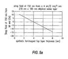
- Fig. 5a shows a calculation of the inter-bit stray field, Hib, at 150 nm emanating from an elliptical synthetic ferrimagnet sense layer 53 as a function of thickness if the bottom layer of the second ferromagnetic layer 47 is 4 nm thick.
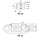
- the inter-bit stray field Hib is shown schematically in figure 5c .
- the sense layer 53 embodiment modeled in Fig. 5a comprises a ferromagnetic layer 55 formed from NiFe(6nm), a spacer layer 49 and a ferromagnetic layer 51 formed of NiFe(4nm).
- the spacer 49 material is a conducting metallic layer of between 0.5 and 2 nm thick and can be formed from Cu, Ru or alloys of various metals.
- a synthetic ferrimagnetic sense layer would produce a smaller stray field at the location of a neighboring bit.
- a 4 nm thick single layer bit would produce an interaction field at 150 nm from the bit end of 15 Oe.
- the stray field at the neighboring bit location decreases and then changes sign.
- the interactions fields again become too large.
- stray fields at the location of neighboring bits are greatly reduced when the top ferromagnetic layer 51 is deposited in the range of 2 nm to 6 nm.
- Fig. 5a shows that the resulting reduction in neighboring bit stray fields would allow magnetic memory bits to be spaced closer in an array 9 with reduced stray field interactions between neighboring bits 11.
- Using only Hd12 and Hd21 to antiferromagnetically couple layers 47 and 51 limits the range of relative layer thickness, which makes it difficult to produce a working sense layer that shows reduced inter-bit interactions.
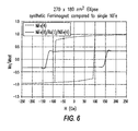
- FIG. 6 shows a comparison of a hysteresis loop for a single 4 nm thick NiFe elliptically patterned sense layer (270 nm x 180 nm) with a hysteresis loop for a synthetic ferrimagnet sense layer 53, similar to that shown in figure 5b , of the same dimension and shape computed using a micromagnetic calculation based on the Landau-Lifshitz-Gilbert equation.
- the coercive magnetic field (Hc) value of the synthetic ferrimagnet sense layer 53 is about 35% higher than the Hc value for the single layer film, and that the magnetic volume of the synthetic ferrimagnet is three times that of the single layer's magnetic volume.
- the required coercive field is not so large that it would require excessively high current to write a magnetic bit 11 sense layer 53.
- the vertical axis in figure 7 refers to the normalized magnetic moment of the synthetic ferrimagnetic sense layer, and the horizontal axis refers to the easy-axis write field.
- This type of plot is often referred to as a hysteresis or M(H) loop. Three H field values of interest are evident in each of the M(H) loops.
- the jump in the M(H) loops that occurs at the field H02 results when both layers 47 and 51 reverse directions simultaneously and thus remain oriented in opposite directions.
- the jump in M that occurs at the fields H01 and H03 results when one of the layers 47 or 51 changes direction independently of the other layer.
- the existence of the jumps at H01 and H03 imply that M1 and M2 can orient in the same direction when the sense layer is written with too strong a write field.
- the synthetic ferrimagnetic sense layer 53 will thus produce larger than desired stray fields Hib. Writing the bit at fields greater than H03 is therefore not desired.
- H01 may approach 0 Oe, in this case the synthetic ferrimagnetic sense layer is unstable, and can magnetize into several undesired states.
- H01, H02, and H03 all depend critically on the values of the parameters Msat1, Msat2, t1, t2, ts, Hc1, and Hc2. It should be noted that all other device parameters being the same, the inclusion of an antiferromagnetic exchange field increases the separation between fields H01 and H02 by moving the fields H01 and H03 to higher values. The antiferromagnetic exchange field also reduces the difference between H01 and H03, an effect which results in a more magnetically stable sense layer. Hexc thus allows greater freedom in synthetic sense layer optimization. If the condition H02 ⁇ H01 is obeyed, it can be shown that a minimum value of Hexc that results in antiparallel orientation of M1 and M2 for all relevant write fields exists.
- Hexc can be used to stabilize an unstable synthetic ferrimagnetic sense layer design, a wider variation in the choice of Msat1, Msat2, t1, and t2 can be accommodated, resulting in the capability to build a sense layer with both improved thermal stability and reduced stray field, Hib.
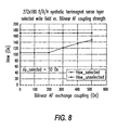
- Figure 8 is used to demonstrate the effect of varying Hexc.
- Figure 8 is a plot of the write field Hsw for a 272 nm by 180 nm elliptical synthetic ferrimagnetic sense layer as a function of Hexc and the hard-axis bias field Hy_selected.
- write margin may be defined as the vertical distance between the Hsw_selected and Hsw_unselected curves. It is desirable to have a large write margin, since this allows the sense layer to be written at a field value that can be chosen to maximize bit yield in an MRAM array. It is evident from figure 8 , that when Hexc ⁇ 200 Oe, there is no change in write margin. As Hexc is increased above 200 Oe, write margin slowly decreases. At some large value of Hexc, write margin becomes zero, and the sense layer cannot be selected for writing without writing all bits located on the same column line.
- Hexc The upper limit in Hexc is strongly dependent on the parameters Msat1, Msat2, t1, t2, ts, Hc1, and Hc2, and it should be determined empirically for each device design. Hexc can be set by proper choice of spacer material, spacer thickness, Msat1, Msat2, t1, and t2.
- the layers in the stack can also be inverted, which may result in a change in the process steps and possibly methods.
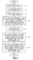
- the pinned or reference layer 43 is deposited at processing segment 113.
- the pinned layer 43 can be a coupled antiferromagnetic and ferromagnetic layer structure, a synthetic ferrimagnet, or an antiferromagnetic layer coupled to a synthetic ferrimagnetic stack.
- the pinned layer 43 materials can be selected from known materials, which are used for pinned layer 43 construction including FeMn, IrMn, PtMn, NiMn, or NiO.
- the pinned layer 43 is smoothed sufficiently by, for example, by sputtering etching or other technique to reduce the magnetic field coupling caused by layer surface irregularities (Neel coupling).
- a thin tunnel barrier layer 45 is deposited.
- the tunnel barrier may be selected from known materials including alumina (Al 2 O 3 ).
- the second ferromagnetic layer 47 is formed from ferromagnetic materials, such as NiFe, so that sufficient antiferromagnetic exchange coupling and stray field 71, 73 coupling is present between the second ferromagnetic layer 47 and the desired third ferromagnetic layer 51 which will be subsequently deposited. Finally, and depending on the choice of materials, the entire stack should be annealed in the presence of a magnetic field, in order to set the correct magnetization orientations for the various layers.
- ferromagnetic materials such as NiFe
- Sufficient antiferromagnetic exchange coupling refers to a sense layer 53 design which provides for antiferromagnetic exchange coupling between the second ferromagnetic layer 47 and the desired third ferromagnetic layer 51 (subsequently formed) such that the antiferromagnetic exchange coupling is more than zero and less than a value which requires a significantly increased magnetic switching field intensity (Hsw) after a certain point of antiferromagnetic exchange coupling of layers 47 and 51 across spacer layer 47.
- Hsw magnetic switching field intensity
- Fig. 8 indicates, given a specified synthetic ferrimagnet dimension and materials, after a certain point of antiferromagnetic exchange coupling (e.g., - 200 Oe), the applied magnetic field (Hx) required to perform a write operation must be increased thereby increasing the current required to perform switching of the sense layer 53 magnetic moment 75, 77 orientations. At some point, when Hexc is too strong, a hard-axis bias (at 90 degrees to the easy axis 19) will not be sufficient to write the magnetic memory bit (11) sense layer 53 (switch the orientation of the sense layer 53 magnetic moments 77, 75).
- Hx antiferromagnetic exchange coupling
- the second ferromagnetic layer 47 may be smoothed to reduce Neel coupling (magnetic coupling between layers 47 and 51 caused by interfacial irregularities) in processing segment 121.
- the spacer element 49 is formed from materials for spacer layers which permit antiferromagnetic exchange coupling including Ru, Cr or Cu, such that sufficient antiferromagnetic exchange coupling and stray field coupling is present across spacer layer 49 between the second ferromagnetic layer 47 and the desired third ferromagnetic layer 51.
- the third ferromagnetic layer 51 is formed from ferromagnetic materials, e.g.
- the antiferromagnetic exchange coupling attribute is dependent upon magnetic memory bit 11 design including sense layer design, bit size and materials and thus may be varied to achieve the desired effect of sufficient antiferromagnetic exchange coupling and magnetic moment switching point separation in the sense layer 53.
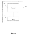
- Fig. 10 shows a processor system 151 comprising a MRAM memory array 9 comprised of magnetic memory bits 11 constructed in accordance with an embodiment of the present invention, coupled with a processor, e.g., a central processor unit 153 for data exchange.
- the magnetic memory bits 11 are electrically coupled to the processor 151 so as to permit reading and writing data to and from the memory bits 11.
- the magnetic memory bits 11 may be coupled to the processor 151 through a memory controller and bus system not pictured or coupled with other components through another data transfer architecture.
Landscapes
- Engineering & Computer Science (AREA)
- Computer Hardware Design (AREA)
- Chemical & Material Sciences (AREA)
- Crystallography & Structural Chemistry (AREA)
- Nanotechnology (AREA)
- Power Engineering (AREA)
- Hall/Mr Elements (AREA)
- Mram Or Spin Memory Techniques (AREA)
- Semiconductor Memories (AREA)
- Luminescent Compositions (AREA)
- Thin Magnetic Films (AREA)
- Magnetic Heads (AREA)
Claims (37)
- Couche de détection pour un élément de mémoire magnétique (11), ladite couche de détection comprenant:une première couche magnétisable (17) avec un moment magnétique orienté dans une première direction;une seconde couche magnétisable (19) avec un moment magnétique orienté dans une seconde direction opposée à ladite première direction;une couche d'espacement (21) formée entre lesdites première et seconde couches magnétisables;lesdites couches étant formées d'un matériau et d'une épaisseur suffisante pour fournir un couplage de champs de dispersion entre lesdites première et seconde couches à travers ladite couche d'espacement de sorte que les première et seconde couches ont des moments magnétiques orientés de manière antiparallèle l'un par rapport à l'autre, caractérisée en ce que:lesdites couches sont formées d'un matériau et d'une épaisseur suffisantes pour fournir un couplage d'échange antiferromagnétique entre les première et seconde couches à travers ladite couche d'espacement de sorte que les moments magnétiques des premier et seconde couches puissent tourner substantiellement simultanément en présence d'un champ magnétique appliqué de sorte que les premier et second moments magnétiques des couches magnétisables puissent être orientés dans l'autre desdites première et seconde directions.
- Couche de détection selon la revendication 1, comprenant en outre :une couche plus mince, par rapport à la première couche magnétisable, de Co interposée entre la couche d'espacement et la première couche magnétisable, etune couche plus fine, par rapport à la seconde couche magnétisable, de Co interposée entre la couche d'espacement et la seconde couche magnétisable.
- Couche de détection selon la revendication 1, comprenant en outre :une couche plus mince, par rapport à la première couche magnétisable, de CoFe interposée entre la couche d'espacement et la première couche magnétisable ; etune couche plus mince, par rapport à la seconde couche magnétisable, de CoFe interposée entre la couche d'espacement et la seconde couche magnétisable.
- Couche de détection selon la revendication 1, dans laquelle les première et seconde couches magnétisables comprennent au moins une couche de NiFe.
- Couche de détection selon la revendication 1, dans laquelle les première et seconde couches magnétisables comprennent au moins une couche de CoFe.
- Couche de détection selon la revendication 1, dans laquelle les première et seconde couches magnétisables comprennent au moins une couche de Co.
- Couche de détection selon la revendication 1, dans laquelle les première et seconde couches magnétisables comprennent au moins une couche de Fe.
- Couche de détection selon la revendication 1, dans laquelle les première et seconde couches magnétisables comprennent au moins une couche de Ni.
- Couche de détection selon la revendication 1, dans laquelle la première et seconde couches magnétisables comprennent au moins une couche de NiFeCo.
- Couche de détection selon la revendication 1, dans laquelle l'épaisseur de la couche d'espacement est telle que le couplage d'échange antiferromagnétique entre les première et seconde couches magnétisables a une valeur de champ magnétique qui est moindre que la valeur du champ coercitif de celle des première et seconde couches magnétisables ayant la valeur de champ coercitif la plus grande.
- Couche de détection selon la revendication 1, dans laquelle la première couche magnétisable a un produit de la saturation magnétique par l'épaisseur de la première couche qui n'est pas égal au produit de la saturation magnétique par l'épaisseur de seconde couche de la seconde couche magnétisable.
- Couche de détection selon la revendication 1, dans laquelle la couche d'espacement est un matériau conducteur.
- Couche de détection selon la revendication 1, dans laquelle la couche d'espacement comprend une couche de Ru.
- Couche de détection selon la revendication 1, dans laquelle la couche d'espacement comprend une couche de Cu.
- Procédé de détection selon la revendication 1, dans lequel ladite couche d'espacement est un conducteur qui n'est pas ferromagnétique ou antiferromagnétique.
- Couche de détection selon la revendication 1, dans laquelle les première et seconde couches magnétisables sont formées de matériaux différents ayant la même épaisseur.
- Couche de détection selon la revendication 1, dans laquelle les première et seconde couches magnétisables sont formées d'un matériau différent, chacun ayant une épaisseur différente de l'autre.
- Couche de détection selon la revendication 1, dans laquelle lesdites couches sont formées selon un modèle elliptique.
- Procédé pour fabriquer un élément de mémoire magnétique, comprenant :la formation d'une couche fixée ou de référence avec une magnétisation dans une première direction supportée par un substrat;la formation d'une couche de barrière de tunnel adjacente à la couche fixée ; etla formation d'une couche de détection adjacente à un côté de la couche de barrière de tunnel faisant face à la couche fixée, ladite couche de détection ayant une première couche ferromagnétique et une seconde couche ferromagnétique séparées mutuellement par une couche d'espacement conductrice et une caractéristique résultant en un couplage de champs de dispersion entre lesdites première et seconde couches ferromagnétiques ;caractérisé en ce que la caractéristique est en outre telle qu'elle résulte en un couplage d'échange antiferromagnétique entre lesdites première et seconde couches ferromagnétiques.
- Procédé selon la revendication 19, dans lequel l'action de former ladite couche de détection comprend en outre : la formation de ladite couche ferromagnétique sur la couche de barrière de tunnel ;
la formation de ladite couche d'espacement conductrice sur la première couche ferromagnétique ; et la formation de la seconde couche ferromagnétique sur la couche d'espacement conductrice. - Procédé selon la revendication 20, comprenant en outre le lissage d'une surface de la couche fixée avant de former une autre couche sur ladite couche fixée.
- Procédé selon la revendication 20, comprenant en outre le lissage de la première couche ferromagnétique avant de former ladite couche d'espacement conductrice.
- Procédé selon la revendication 20, dans lequel lesdites première et seconde couches ferromagnétiques sont formées d'un matériau comprenant du NiFe.
- Procédé selon la revendication 20, dans lequel lesdites première et seconde couches ferromagnétiques sont formées d'un matériau comprenant du CoFe.
- Procédé selon la revendication 20, dans lequel lesdites première et seconde couches ferromagnétiques sont formées d'un matériau comprenant du Co.
- Procédé selon la revendication 20, dans lequel lesdites première et seconde couches ferromagnétiques sont formées d'un matériau comprenant du Fe.
- Procédé selon la revendication 20, dans lequel lesdites première et seconde couches ferromagnétiques sont formées d'un matériau comprenant du Ni.
- Procédé selon la revendication 20, dans lequel lesdites première et seconde couches ferromagnétiques sont formées d'un matériau comprenant du NiFeCo.
- Procédé selon la revendication 20, dans lequel ladite couche d'espacement conductrice comprend une couche de Ru.
- Procédé selon la revendication 20, dans lequel ladite couche d'espacement conductrice comprend une couche de Cu.
- Procédé selon la revendication 20, dans lequel ladite couche d'espacement est un conducteur qui n'est pas ferromagnétique ou antiferromagnétique.
- Procédé selon la revendication 20, dans lequel ladite couche d'espacement conductrice a une épaisseur telle que le couplage d'échange antiferromagnétique entre lesdites première et seconde couches ferromagnétiques est moindre que la valeur de champ coercitif (H) de celle des première et seconde couches ferromagnétiques qui a la valeur de champ coercitif la plus grande.
- Procédé selon la revendication 20, dans lequel la formation desdites couches est telle que les couches sont formées d'un matériau et d'une épaisseur suffisantes pour fournir un couplage de champs de dispersion et un couplage d'échange antiferromagnétique, ledit couplage d'échange antiferromagnétique est dans la plage de 0 à ≤200 Oe entre les première et seconde couches ferromagnétiques à travers ladite couche d'espacement conductrice.
- Procédé selon la revendication 20, dans lequel ladite étape consistant à former les première et seconde couches ferromagnétiques inclut la formation desdites première et seconde couches incluant le NiFe.
- Procédé selon la revendication 20, dans lequel la seconde couche est formée avec une épaisseur t et la première couche est formée avec une épaisseur plus grande que t.
- Procédé selon la revendication 20, comprenant en outre :la formation d'une couche plus mince, par rapport à la première couche ferromagnétique, de Co interposée entre la couche d'espacement conductrice et la première couche ferromagnétique ; etla formation d'une couche plus mince, par rapport à la seconde couche ferromagnétique, de Co interposée entre la couche d'espacement conductrice et la seconde couche ferromagnétique.
- Procédé selon la revendication 20, comprenant en outre :la formation d'une couche plus mince, par rapport à la première couche ferromagnétique, de CoFe interposée entre la couche d'espacement conductrice et la première couche ferromagnétique; etla formation d'une couche plus mince, par rapport à la seconde couche ferromagnétique, de CoFe interposée entre la couche d'espacement conductrice et la seconde couche ferromagnétique.
Priority Applications (1)
| Application Number | Priority Date | Filing Date | Title |
|---|---|---|---|
| EP08019584A EP2053613A1 (fr) | 2002-04-03 | 2003-03-14 | Couche de détection synthétique-ferrimagnétique pour applications MRAM haute densité |
Applications Claiming Priority (3)
| Application Number | Priority Date | Filing Date | Title |
|---|---|---|---|
| US114249 | 2002-04-03 | ||
| US10/114,249 US6728132B2 (en) | 2002-04-03 | 2002-04-03 | Synthetic-ferrimagnet sense-layer for high density MRAM applications |
| PCT/US2003/007843 WO2003085674A2 (fr) | 2002-04-03 | 2003-03-14 | Couche de detection ferrimagnetique synthetique pour applications magnetiques a acces aleatoire (mram) |
Related Child Applications (1)
| Application Number | Title | Priority Date | Filing Date |
|---|---|---|---|
| EP08019584A Division EP2053613A1 (fr) | 2002-04-03 | 2003-03-14 | Couche de détection synthétique-ferrimagnétique pour applications MRAM haute densité |
Publications (2)
| Publication Number | Publication Date |
|---|---|
| EP1490877A2 EP1490877A2 (fr) | 2004-12-29 |
| EP1490877B1 true EP1490877B1 (fr) | 2009-01-21 |
Family
ID=28673684
Family Applications (2)
| Application Number | Title | Priority Date | Filing Date |
|---|---|---|---|
| EP03746039A Expired - Lifetime EP1490877B1 (fr) | 2002-04-03 | 2003-03-14 | Couche de detection ferrimagnetique synthetique pour applications magnetiques a acces aleatoire (mram) |
| EP08019584A Ceased EP2053613A1 (fr) | 2002-04-03 | 2003-03-14 | Couche de détection synthétique-ferrimagnétique pour applications MRAM haute densité |
Family Applications After (1)
| Application Number | Title | Priority Date | Filing Date |
|---|---|---|---|
| EP08019584A Ceased EP2053613A1 (fr) | 2002-04-03 | 2003-03-14 | Couche de détection synthétique-ferrimagnétique pour applications MRAM haute densité |
Country Status (10)
| Country | Link |
|---|---|
| US (2) | US6728132B2 (fr) |
| EP (2) | EP1490877B1 (fr) |
| JP (1) | JP2005522044A (fr) |
| KR (1) | KR100624762B1 (fr) |
| CN (1) | CN100576344C (fr) |
| AT (1) | ATE421756T1 (fr) |
| AU (1) | AU2003225795A1 (fr) |
| DE (1) | DE60325948D1 (fr) |
| TW (1) | TWI287871B (fr) |
| WO (1) | WO2003085674A2 (fr) |
Families Citing this family (27)
| Publication number | Priority date | Publication date | Assignee | Title |
|---|---|---|---|---|
| DE10214159B4 (de) * | 2002-03-28 | 2008-03-20 | Qimonda Ag | Verfahren zur Herstellung einer Referenzschicht für MRAM-Speicherzellen |
| US7054118B2 (en) * | 2002-03-28 | 2006-05-30 | Nve Corporation | Superparamagnetic field sensing devices |
| US6724652B2 (en) | 2002-05-02 | 2004-04-20 | Micron Technology, Inc. | Low remanence flux concentrator for MRAM devices |
| US6885576B2 (en) * | 2002-08-13 | 2005-04-26 | Micron Technology, Inc. | Closed flux magnetic memory |
| JP2004111437A (ja) * | 2002-09-13 | 2004-04-08 | Toshiba Corp | 磁気記憶装置 |
| JP2004179483A (ja) * | 2002-11-28 | 2004-06-24 | Hitachi Ltd | 不揮発性磁気メモリ |
| US7002228B2 (en) | 2003-02-18 | 2006-02-21 | Micron Technology, Inc. | Diffusion barrier for improving the thermal stability of MRAM devices |
| US7020009B2 (en) * | 2003-05-14 | 2006-03-28 | Macronix International Co., Ltd. | Bistable magnetic device using soft magnetic intermediary material |
| US6865105B1 (en) * | 2003-09-22 | 2005-03-08 | Hewlett-Packard Development Company, L.P. | Thermal-assisted switching array configuration for MRAM |
| JP5015600B2 (ja) * | 2003-10-14 | 2012-08-29 | エージェンシー フォー サイエンス,テクノロジー アンド リサーチ | 磁気メモリデバイス |
| US7045838B2 (en) * | 2003-10-31 | 2006-05-16 | International Business Machines Corporation | Techniques for coupling in semiconductor devices and magnetic device using these techniques |
| US7053430B2 (en) * | 2003-11-12 | 2006-05-30 | Honeywell International Inc. | Antiferromagnetic stabilized storage layers in GMRAM storage devices |
| US7602000B2 (en) * | 2003-11-19 | 2009-10-13 | International Business Machines Corporation | Spin-current switched magnetic memory element suitable for circuit integration and method of fabricating the memory element |
| US7072209B2 (en) * | 2003-12-29 | 2006-07-04 | Micron Technology, Inc. | Magnetic memory having synthetic antiferromagnetic pinned layer |
| US7105372B2 (en) * | 2004-01-20 | 2006-09-12 | Headway Technologies, Inc. | Magnetic tunneling junction film structure with process determined in-plane magnetic anisotropy |
| US7183893B2 (en) * | 2004-02-04 | 2007-02-27 | Seagate Technology Llc | TMR sensor with oxidized alloy barrier layer and method for forming the same |
| TWI283477B (en) * | 2004-11-16 | 2007-07-01 | Ind Tech Res Inst | Magnetic random access memory with lower switching field |
| TWI278989B (en) * | 2004-12-29 | 2007-04-11 | Ind Tech Res Inst | Magnetic random access memory with lower switching field through indirect exchange coupling |
| TWI277761B (en) * | 2006-03-20 | 2007-04-01 | Univ Nat Yunlin Sci & Tech | Method for measuring hysteresis curve and anisotropic energy of magnetic memory units |
| JP5146836B2 (ja) * | 2006-12-06 | 2013-02-20 | 日本電気株式会社 | 磁気ランダムアクセスメモリ及びその製造方法 |
| US7486551B1 (en) * | 2007-04-03 | 2009-02-03 | Grandis, Inc. | Method and system for providing domain wall assisted switching of magnetic elements and magnetic memories using such magnetic elements |
| CN102270736B (zh) * | 2010-06-01 | 2014-02-05 | 中国科学院物理研究所 | 一种用于磁敏传感器的磁性纳米多层膜及其制造方法 |
| JP5786341B2 (ja) * | 2010-09-06 | 2015-09-30 | ソニー株式会社 | 記憶素子、メモリ装置 |
| JP2012209358A (ja) * | 2011-03-29 | 2012-10-25 | Renesas Electronics Corp | 磁気記憶素子および磁気記憶装置 |
| EP2775480B1 (fr) * | 2013-03-07 | 2018-11-14 | Crocus Technology S.A. | Cellule de mémoire TAS-MRAM autoréférencée qui peut être lue avec une consommation d'énergie réduite |
| EP3104187A1 (fr) * | 2015-06-09 | 2016-12-14 | International Iberian Nanotechnology Laboratory | Capteur magnéto-résistant |
| KR102433703B1 (ko) * | 2015-11-30 | 2022-08-19 | 에스케이하이닉스 주식회사 | 전자 장치 |
Family Cites Families (21)
| Publication number | Priority date | Publication date | Assignee | Title |
|---|---|---|---|---|
| US5173873A (en) | 1990-06-28 | 1992-12-22 | The United States Of America As Represented By The Administrator Of The National Aeronautics And Space Administration | High speed magneto-resistive random access memory |
| US5764567A (en) * | 1996-11-27 | 1998-06-09 | International Business Machines Corporation | Magnetic tunnel junction device with nonferromagnetic interface layer for improved magnetic field response |
| US5650958A (en) | 1996-03-18 | 1997-07-22 | International Business Machines Corporation | Magnetic tunnel junctions with controlled magnetic response |
| US5768181A (en) | 1997-04-07 | 1998-06-16 | Motorola, Inc. | Magnetic device having multi-layer with insulating and conductive layers |
| US6028786A (en) * | 1997-04-28 | 2000-02-22 | Canon Kabushiki Kaisha | Magnetic memory element having coupled magnetic layers forming closed magnetic circuit |
| US5966012A (en) | 1997-10-07 | 1999-10-12 | International Business Machines Corporation | Magnetic tunnel junction device with improved fixed and free ferromagnetic layers |
| US5982658A (en) | 1997-10-31 | 1999-11-09 | Honeywell Inc. | MRAM design to reduce dissimilar nearest neighbor effects |
| US6252796B1 (en) * | 1998-08-14 | 2001-06-26 | U.S. Philips Corporation | Device comprising a first and a second ferromagnetic layer separated by a non-magnetic spacer layer |
| US6219212B1 (en) | 1998-09-08 | 2001-04-17 | International Business Machines Corporation | Magnetic tunnel junction head structure with insulating antiferromagnetic layer |
| US6365286B1 (en) * | 1998-09-11 | 2002-04-02 | Kabushiki Kaisha Toshiba | Magnetic element, magnetic memory device, magnetoresistance effect head, and magnetic storage system |
| US6436526B1 (en) * | 1999-06-17 | 2002-08-20 | Matsushita Electric Industrial Co., Ltd. | Magneto-resistance effect element, magneto-resistance effect memory cell, MRAM and method for performing information write to or read from the magneto-resistance effect memory cell |
| US6166948A (en) | 1999-09-03 | 2000-12-26 | International Business Machines Corporation | Magnetic memory array with magnetic tunnel junction memory cells having flux-closed free layers |
| JP2001156357A (ja) * | 1999-09-16 | 2001-06-08 | Toshiba Corp | 磁気抵抗効果素子および磁気記録素子 |
| JP3891540B2 (ja) * | 1999-10-25 | 2007-03-14 | キヤノン株式会社 | 磁気抵抗効果メモリ、磁気抵抗効果メモリに記録される情報の記録再生方法、およびmram |
| US6233172B1 (en) * | 1999-12-17 | 2001-05-15 | Motorola, Inc. | Magnetic element with dual magnetic states and fabrication method thereof |
| JP2001196658A (ja) * | 2000-01-07 | 2001-07-19 | Fujitsu Ltd | 磁気素子及び磁気記憶装置 |
| US6590806B1 (en) * | 2000-03-09 | 2003-07-08 | Hewlett-Packard Development Company, L.P. | Multibit magnetic memory element |
| US6469926B1 (en) * | 2000-03-22 | 2002-10-22 | Motorola, Inc. | Magnetic element with an improved magnetoresistance ratio and fabricating method thereof |
| EP1187103A3 (fr) * | 2000-08-04 | 2003-01-08 | Matsushita Electric Industrial Co., Ltd. | Dispositif à effet magnétorésistif, tête et élément de mémoire |
| US6767655B2 (en) * | 2000-08-21 | 2004-07-27 | Matsushita Electric Industrial Co., Ltd. | Magneto-resistive element |
| US6404674B1 (en) * | 2001-04-02 | 2002-06-11 | Hewlett Packard Company Intellectual Property Administrator | Cladded read-write conductor for a pinned-on-the-fly soft reference layer |
-
2002
- 2002-04-03 US US10/114,249 patent/US6728132B2/en not_active Expired - Lifetime
-
2003
- 2003-03-14 JP JP2003582772A patent/JP2005522044A/ja active Pending
- 2003-03-14 CN CN03807585A patent/CN100576344C/zh not_active Expired - Lifetime
- 2003-03-14 AT AT03746039T patent/ATE421756T1/de not_active IP Right Cessation
- 2003-03-14 AU AU2003225795A patent/AU2003225795A1/en not_active Abandoned
- 2003-03-14 EP EP03746039A patent/EP1490877B1/fr not_active Expired - Lifetime
- 2003-03-14 KR KR1020047015785A patent/KR100624762B1/ko not_active Expired - Lifetime
- 2003-03-14 EP EP08019584A patent/EP2053613A1/fr not_active Ceased
- 2003-03-14 WO PCT/US2003/007843 patent/WO2003085674A2/fr not_active Ceased
- 2003-03-14 DE DE60325948T patent/DE60325948D1/de not_active Expired - Lifetime
- 2003-03-28 TW TW092107109A patent/TWI287871B/zh not_active IP Right Cessation
-
2004
- 2004-01-23 US US10/762,478 patent/US6946302B2/en not_active Expired - Lifetime
Also Published As
| Publication number | Publication date |
|---|---|
| CN100576344C (zh) | 2009-12-30 |
| TWI287871B (en) | 2007-10-01 |
| AU2003225795A1 (en) | 2003-10-20 |
| CN1647208A (zh) | 2005-07-27 |
| TW200306004A (en) | 2003-11-01 |
| EP1490877A2 (fr) | 2004-12-29 |
| WO2003085674A3 (fr) | 2004-02-12 |
| JP2005522044A (ja) | 2005-07-21 |
| KR100624762B1 (ko) | 2006-09-19 |
| US6946302B2 (en) | 2005-09-20 |
| WO2003085674A2 (fr) | 2003-10-16 |
| AU2003225795A8 (en) | 2003-10-20 |
| DE60325948D1 (de) | 2009-03-12 |
| KR20040101391A (ko) | 2004-12-02 |
| EP2053613A1 (fr) | 2009-04-29 |
| US20030189842A1 (en) | 2003-10-09 |
| ATE421756T1 (de) | 2009-02-15 |
| US6728132B2 (en) | 2004-04-27 |
| US20040152218A1 (en) | 2004-08-05 |
Similar Documents
| Publication | Publication Date | Title |
|---|---|---|
| EP1490877B1 (fr) | Couche de detection ferrimagnetique synthetique pour applications magnetiques a acces aleatoire (mram) | |
| US6833278B2 (en) | Low remanence flux concentrator for MRAM devices | |
| US7881099B2 (en) | Multibit magnetic random access memory device | |
| US7227773B1 (en) | Magnetic element utilizing spin-transfer and half-metals and an MRAM device using the magnetic element | |
| US5966323A (en) | Low switching field magnetoresistive tunneling junction for high density arrays | |
| US7072208B2 (en) | Vortex magnetic random access memory | |
| US20040090844A1 (en) | Multi-bit magnetic memory cells | |
| US8198660B2 (en) | Multi-bit STRAM memory cells | |
| US7799581B2 (en) | Methods of forming magnetic memory devices | |
| US20050167657A1 (en) | Multi-bit magnetic memory cells | |
| US7630231B2 (en) | Hybrid memory cell for spin-polarized electron current induced switching and writing/reading process using such memory cell | |
| US8482970B2 (en) | Multi-bit STRAM memory cells | |
| US6735112B2 (en) | Magneto-resistive memory cell structures with improved selectivity |
Legal Events
| Date | Code | Title | Description |
|---|---|---|---|
| PUAI | Public reference made under article 153(3) epc to a published international application that has entered the european phase |
Free format text: ORIGINAL CODE: 0009012 |
|
| 17P | Request for examination filed |
Effective date: 20040927 |
|
| AK | Designated contracting states |
Kind code of ref document: A2 Designated state(s): AT BE BG CH CY CZ DE DK EE ES FI FR GB GR HU IE IT LI LU MC NL PT RO SE SI SK TR |
|
| AX | Request for extension of the european patent |
Extension state: AL LT LV MK |
|
| RIN1 | Information on inventor provided before grant (corrected) |
Inventor name: DEAK, JAMES, G. |
|
| 17Q | First examination report despatched |
Effective date: 20061222 |
|
| GRAP | Despatch of communication of intention to grant a patent |
Free format text: ORIGINAL CODE: EPIDOSNIGR1 |
|
| GRAS | Grant fee paid |
Free format text: ORIGINAL CODE: EPIDOSNIGR3 |
|
| GRAA | (expected) grant |
Free format text: ORIGINAL CODE: 0009210 |
|
| AK | Designated contracting states |
Kind code of ref document: B1 Designated state(s): AT BE BG CH CY CZ DE DK EE ES FI FR GB GR HU IE IT LI LU MC NL PT RO SE SI SK TR |
|
| REG | Reference to a national code |
Ref country code: GB Ref legal event code: FG4D |
|
| REG | Reference to a national code |
Ref country code: CH Ref legal event code: EP |
|
| REG | Reference to a national code |
Ref country code: IE Ref legal event code: FG4D |
|
| REF | Corresponds to: |
Ref document number: 60325948 Country of ref document: DE Date of ref document: 20090312 Kind code of ref document: P |
|
| PG25 | Lapsed in a contracting state [announced via postgrant information from national office to epo] |
Ref country code: NL Free format text: LAPSE BECAUSE OF FAILURE TO SUBMIT A TRANSLATION OF THE DESCRIPTION OR TO PAY THE FEE WITHIN THE PRESCRIBED TIME-LIMIT Effective date: 20090121 |
|
| NLV1 | Nl: lapsed or annulled due to failure to fulfill the requirements of art. 29p and 29m of the patents act | ||
| PG25 | Lapsed in a contracting state [announced via postgrant information from national office to epo] |
Ref country code: ES Free format text: LAPSE BECAUSE OF FAILURE TO SUBMIT A TRANSLATION OF THE DESCRIPTION OR TO PAY THE FEE WITHIN THE PRESCRIBED TIME-LIMIT Effective date: 20090502 Ref country code: SI Free format text: LAPSE BECAUSE OF FAILURE TO SUBMIT A TRANSLATION OF THE DESCRIPTION OR TO PAY THE FEE WITHIN THE PRESCRIBED TIME-LIMIT Effective date: 20090121 Ref country code: FI Free format text: LAPSE BECAUSE OF FAILURE TO SUBMIT A TRANSLATION OF THE DESCRIPTION OR TO PAY THE FEE WITHIN THE PRESCRIBED TIME-LIMIT Effective date: 20090121 |
|
| PG25 | Lapsed in a contracting state [announced via postgrant information from national office to epo] |
Ref country code: SE Free format text: LAPSE BECAUSE OF FAILURE TO SUBMIT A TRANSLATION OF THE DESCRIPTION OR TO PAY THE FEE WITHIN THE PRESCRIBED TIME-LIMIT Effective date: 20090421 Ref country code: PT Free format text: LAPSE BECAUSE OF FAILURE TO SUBMIT A TRANSLATION OF THE DESCRIPTION OR TO PAY THE FEE WITHIN THE PRESCRIBED TIME-LIMIT Effective date: 20090622 Ref country code: AT Free format text: LAPSE BECAUSE OF FAILURE TO SUBMIT A TRANSLATION OF THE DESCRIPTION OR TO PAY THE FEE WITHIN THE PRESCRIBED TIME-LIMIT Effective date: 20090121 |
|
| PG25 | Lapsed in a contracting state [announced via postgrant information from national office to epo] |
Ref country code: BE Free format text: LAPSE BECAUSE OF FAILURE TO SUBMIT A TRANSLATION OF THE DESCRIPTION OR TO PAY THE FEE WITHIN THE PRESCRIBED TIME-LIMIT Effective date: 20090121 |
|
| PG25 | Lapsed in a contracting state [announced via postgrant information from national office to epo] |
Ref country code: EE Free format text: LAPSE BECAUSE OF FAILURE TO SUBMIT A TRANSLATION OF THE DESCRIPTION OR TO PAY THE FEE WITHIN THE PRESCRIBED TIME-LIMIT Effective date: 20090121 Ref country code: CZ Free format text: LAPSE BECAUSE OF FAILURE TO SUBMIT A TRANSLATION OF THE DESCRIPTION OR TO PAY THE FEE WITHIN THE PRESCRIBED TIME-LIMIT Effective date: 20090121 Ref country code: MC Free format text: LAPSE BECAUSE OF NON-PAYMENT OF DUE FEES Effective date: 20090331 Ref country code: DK Free format text: LAPSE BECAUSE OF FAILURE TO SUBMIT A TRANSLATION OF THE DESCRIPTION OR TO PAY THE FEE WITHIN THE PRESCRIBED TIME-LIMIT Effective date: 20090121 |
|
| REG | Reference to a national code |
Ref country code: CH Ref legal event code: PL |
|
| PLBE | No opposition filed within time limit |
Free format text: ORIGINAL CODE: 0009261 |
|
| STAA | Information on the status of an ep patent application or granted ep patent |
Free format text: STATUS: NO OPPOSITION FILED WITHIN TIME LIMIT |
|
| PG25 | Lapsed in a contracting state [announced via postgrant information from national office to epo] |
Ref country code: RO Free format text: LAPSE BECAUSE OF FAILURE TO SUBMIT A TRANSLATION OF THE DESCRIPTION OR TO PAY THE FEE WITHIN THE PRESCRIBED TIME-LIMIT Effective date: 20090121 Ref country code: SK Free format text: LAPSE BECAUSE OF FAILURE TO SUBMIT A TRANSLATION OF THE DESCRIPTION OR TO PAY THE FEE WITHIN THE PRESCRIBED TIME-LIMIT Effective date: 20090121 |
|
| REG | Reference to a national code |
Ref country code: FR Ref legal event code: ST Effective date: 20091130 |
|
| 26N | No opposition filed |
Effective date: 20091022 |
|
| PG25 | Lapsed in a contracting state [announced via postgrant information from national office to epo] |
Ref country code: IE Free format text: LAPSE BECAUSE OF NON-PAYMENT OF DUE FEES Effective date: 20090314 Ref country code: LI Free format text: LAPSE BECAUSE OF NON-PAYMENT OF DUE FEES Effective date: 20090331 Ref country code: BG Free format text: LAPSE BECAUSE OF FAILURE TO SUBMIT A TRANSLATION OF THE DESCRIPTION OR TO PAY THE FEE WITHIN THE PRESCRIBED TIME-LIMIT Effective date: 20090421 Ref country code: CH Free format text: LAPSE BECAUSE OF NON-PAYMENT OF DUE FEES Effective date: 20090331 |
|
| PG25 | Lapsed in a contracting state [announced via postgrant information from national office to epo] |
Ref country code: FR Free format text: LAPSE BECAUSE OF NON-PAYMENT OF DUE FEES Effective date: 20091123 |
|
| PG25 | Lapsed in a contracting state [announced via postgrant information from national office to epo] |
Ref country code: GR Free format text: LAPSE BECAUSE OF FAILURE TO SUBMIT A TRANSLATION OF THE DESCRIPTION OR TO PAY THE FEE WITHIN THE PRESCRIBED TIME-LIMIT Effective date: 20090422 |
|
| PG25 | Lapsed in a contracting state [announced via postgrant information from national office to epo] |
Ref country code: LU Free format text: LAPSE BECAUSE OF NON-PAYMENT OF DUE FEES Effective date: 20090314 |
|
| PG25 | Lapsed in a contracting state [announced via postgrant information from national office to epo] |
Ref country code: HU Free format text: LAPSE BECAUSE OF FAILURE TO SUBMIT A TRANSLATION OF THE DESCRIPTION OR TO PAY THE FEE WITHIN THE PRESCRIBED TIME-LIMIT Effective date: 20090722 |
|
| PG25 | Lapsed in a contracting state [announced via postgrant information from national office to epo] |
Ref country code: TR Free format text: LAPSE BECAUSE OF FAILURE TO SUBMIT A TRANSLATION OF THE DESCRIPTION OR TO PAY THE FEE WITHIN THE PRESCRIBED TIME-LIMIT Effective date: 20090121 |
|
| PG25 | Lapsed in a contracting state [announced via postgrant information from national office to epo] |
Ref country code: CY Free format text: LAPSE BECAUSE OF FAILURE TO SUBMIT A TRANSLATION OF THE DESCRIPTION OR TO PAY THE FEE WITHIN THE PRESCRIBED TIME-LIMIT Effective date: 20090121 |
|
| PGFP | Annual fee paid to national office [announced via postgrant information from national office to epo] |
Ref country code: GB Payment date: 20130313 Year of fee payment: 11 |
|
| GBPC | Gb: european patent ceased through non-payment of renewal fee |
Effective date: 20140314 |
|
| PG25 | Lapsed in a contracting state [announced via postgrant information from national office to epo] |
Ref country code: GB Free format text: LAPSE BECAUSE OF NON-PAYMENT OF DUE FEES Effective date: 20140314 |
|
| PGFP | Annual fee paid to national office [announced via postgrant information from national office to epo] |
Ref country code: DE Payment date: 20220329 Year of fee payment: 20 |
|
| PGFP | Annual fee paid to national office [announced via postgrant information from national office to epo] |
Ref country code: IT Payment date: 20220322 Year of fee payment: 20 |
|
| REG | Reference to a national code |
Ref country code: DE Ref legal event code: R071 Ref document number: 60325948 Country of ref document: DE |