EP1492076A2 - Ansteuerschaltung und Verfahren für eine Plasmaanzeigetafel - Google Patents
Ansteuerschaltung und Verfahren für eine Plasmaanzeigetafel Download PDFInfo
- Publication number
- EP1492076A2 EP1492076A2 EP20040090250 EP04090250A EP1492076A2 EP 1492076 A2 EP1492076 A2 EP 1492076A2 EP 20040090250 EP20040090250 EP 20040090250 EP 04090250 A EP04090250 A EP 04090250A EP 1492076 A2 EP1492076 A2 EP 1492076A2
- Authority
- EP
- European Patent Office
- Prior art keywords
- voltage
- capacitor
- transistor
- driving device
- coupled
- Prior art date
- Legal status (The legal status is an assumption and is not a legal conclusion. Google has not performed a legal analysis and makes no representation as to the accuracy of the status listed.)
- Granted
Links
Images







Classifications
-
- G—PHYSICS
- G09—EDUCATION; CRYPTOGRAPHY; DISPLAY; ADVERTISING; SEALS
- G09G—ARRANGEMENTS OR CIRCUITS FOR CONTROL OF INDICATING DEVICES USING STATIC MEANS TO PRESENT VARIABLE INFORMATION
- G09G3/00—Control arrangements or circuits, of interest only in connection with visual indicators other than cathode-ray tubes
- G09G3/20—Control arrangements or circuits, of interest only in connection with visual indicators other than cathode-ray tubes for presentation of an assembly of a number of characters, e.g. a page, by composing the assembly by combination of individual elements arranged in a matrix no fixed position being assigned to or needed to be assigned to the individual characters or partial characters
- G09G3/22—Control arrangements or circuits, of interest only in connection with visual indicators other than cathode-ray tubes for presentation of an assembly of a number of characters, e.g. a page, by composing the assembly by combination of individual elements arranged in a matrix no fixed position being assigned to or needed to be assigned to the individual characters or partial characters using controlled light sources
- G09G3/28—Control arrangements or circuits, of interest only in connection with visual indicators other than cathode-ray tubes for presentation of an assembly of a number of characters, e.g. a page, by composing the assembly by combination of individual elements arranged in a matrix no fixed position being assigned to or needed to be assigned to the individual characters or partial characters using controlled light sources using luminous gas-discharge panels, e.g. plasma panels
- G09G3/288—Control arrangements or circuits, of interest only in connection with visual indicators other than cathode-ray tubes for presentation of an assembly of a number of characters, e.g. a page, by composing the assembly by combination of individual elements arranged in a matrix no fixed position being assigned to or needed to be assigned to the individual characters or partial characters using controlled light sources using luminous gas-discharge panels, e.g. plasma panels using AC panels
- G09G3/296—Driving circuits for producing the waveforms applied to the driving electrodes
-
- G—PHYSICS
- G09—EDUCATION; CRYPTOGRAPHY; DISPLAY; ADVERTISING; SEALS
- G09G—ARRANGEMENTS OR CIRCUITS FOR CONTROL OF INDICATING DEVICES USING STATIC MEANS TO PRESENT VARIABLE INFORMATION
- G09G3/00—Control arrangements or circuits, of interest only in connection with visual indicators other than cathode-ray tubes
- G09G3/20—Control arrangements or circuits, of interest only in connection with visual indicators other than cathode-ray tubes for presentation of an assembly of a number of characters, e.g. a page, by composing the assembly by combination of individual elements arranged in a matrix no fixed position being assigned to or needed to be assigned to the individual characters or partial characters
- G09G3/22—Control arrangements or circuits, of interest only in connection with visual indicators other than cathode-ray tubes for presentation of an assembly of a number of characters, e.g. a page, by composing the assembly by combination of individual elements arranged in a matrix no fixed position being assigned to or needed to be assigned to the individual characters or partial characters using controlled light sources
- G09G3/28—Control arrangements or circuits, of interest only in connection with visual indicators other than cathode-ray tubes for presentation of an assembly of a number of characters, e.g. a page, by composing the assembly by combination of individual elements arranged in a matrix no fixed position being assigned to or needed to be assigned to the individual characters or partial characters using controlled light sources using luminous gas-discharge panels, e.g. plasma panels
- G09G3/288—Control arrangements or circuits, of interest only in connection with visual indicators other than cathode-ray tubes for presentation of an assembly of a number of characters, e.g. a page, by composing the assembly by combination of individual elements arranged in a matrix no fixed position being assigned to or needed to be assigned to the individual characters or partial characters using controlled light sources using luminous gas-discharge panels, e.g. plasma panels using AC panels
- G09G3/291—Control arrangements or circuits, of interest only in connection with visual indicators other than cathode-ray tubes for presentation of an assembly of a number of characters, e.g. a page, by composing the assembly by combination of individual elements arranged in a matrix no fixed position being assigned to or needed to be assigned to the individual characters or partial characters using controlled light sources using luminous gas-discharge panels, e.g. plasma panels using AC panels controlling the gas discharge to control a cell condition, e.g. by means of specific pulse shapes
- G09G3/292—Control arrangements or circuits, of interest only in connection with visual indicators other than cathode-ray tubes for presentation of an assembly of a number of characters, e.g. a page, by composing the assembly by combination of individual elements arranged in a matrix no fixed position being assigned to or needed to be assigned to the individual characters or partial characters using controlled light sources using luminous gas-discharge panels, e.g. plasma panels using AC panels controlling the gas discharge to control a cell condition, e.g. by means of specific pulse shapes for reset discharge, priming discharge or erase discharge occurring in a phase other than addressing
- G09G3/2927—Details of initialising
-
- G—PHYSICS
- G09—EDUCATION; CRYPTOGRAPHY; DISPLAY; ADVERTISING; SEALS
- G09G—ARRANGEMENTS OR CIRCUITS FOR CONTROL OF INDICATING DEVICES USING STATIC MEANS TO PRESENT VARIABLE INFORMATION
- G09G2310/00—Command of the display device
- G09G2310/06—Details of flat display driving waveforms
- G09G2310/066—Waveforms comprising a gently increasing or decreasing portion, e.g. ramp
Definitions
- the present invention relates to a driving device and method for a plasma display panel (PDP).
- PDP plasma display panel
- a PDP is a flat panel display for displaying characters or images using the plasma generated by gas discharge, and several tens to several millions of pixels are arranged in a matrix format on the PDP depending on the PDP size.
- the PDP is classified as a DC PDP or an AC PDP depending on the waveforms of applied driving voltages and the configurations of discharge cells.
- the AC PDP driving method uses a reset period, an address period, and a sustain period sequentially.
- wall charges formed during a previous sustain period are erased, and cells are reset so as to readily perform the next address operation.
- the address period cells that are turned on and those that are not turned on are selected, and wall charges are accumulated on the turned-on cells (i.e., addressed cells).
- the sustain period a discharge is created in the addressed cells that allows the addressed cells to take part in image display.
- sustain pulses are alternately applied to the scan electrodes and sustain electrodes to sustain the discharge and display the images.
- wall charges refers to charges that accumulate on the electrodes and are formed proximate to the electrodes on the wall (e.g., dielectric layer) of the discharge DCis.
- the wall charges typically do not actually touch the electrodes themselves because a dielectric layer covers the electrodes. However, for simplicity in description, the charges will be described herein as being “formed on”, “stored on” and/or “accumulated on” the electrodes. Furthermore, the term wall voltage, as used herein, refers to a voltage potential that exists on the wall of discharge cells. The wall voltage is caused by the wall charges.
- a ramp waveform is applied to a scan electrode so as to establish wall charges in the reset period, as disclosed in US Patent No. 5,745,086. Specifically, a rising ramp waveform which gradually rises is applied to the scan electrode, followed by a falling ramp waveform which gradually falls. Since precise control of the wall charges greatly depends on the gradient of the ramp if ramp waveforms are applied, the wall charges are typically not controlled precisely during any given time frame.
- Embodiments of the present invention provide PDP driving devices and methods for precisely controlling wall charges.
- Embodiments according to one aspect of the present invention provide a driving device for a plasma display panel.
- the plasma display panel has a capacitive load formed by at least two electrodes.
- the driving device comprises a transistor and a capacitor.
- the transistor has a first main end coupled to the capacitive load, a second main end coupled to a power source for supplying a first voltage, and a control end, and is turned on in response to a first level of a control signal applied to the control end.
- the capacitor is provided in a path including the capacitive load, the transistor, and the voltage source.
- the voltage of the capacitive load is changed by the voltage difference between the voltage source and the capacitive ioad when the transistor is turned on.
- the transistor is turned off when the capacitor is charged to a second voltage while the voltage of the capacitive load is changed.
- Embodiments according to another aspect of the present invention provide a driving device for a plasma display panel.
- the plasma display panel has a capacitive load formed by at least two electrodes.
- the driving device comprises a transistor, a capacitor, a control voltage source, and a discharge path.
- the transistor has a first main end coupled to the capacitive load.
- the capacitor has a first end coupled to a second main end of the transistor and a second end coupled to a voltage source supplying a first voltage.
- the control voltage source supplies a control voltage to a control end of the transistor.
- the discharge path has a first end coupled to the first end of the capacitor. The state of the transistor is determined by the first end voltage of the capacitor.
- Embodiments according to still another aspect of the present invention provide a driving device of a plasma display panel.
- the plasma display panel has a capacitive load formed by at least two electrodes.
- the driving device comprises a transistor, a capacitor, a control voltage source, and a discharge path.
- the transistor has a first main end coupled to a voltage source supplying a first voltage.
- the capacitor has a first end coupled to a second main end of the transistor and a second end coupled to the capacitive load.
- the control voltage source supplies a control voltage to a control end of the transistor.
- the discharge path has a first end coupled to the first end of the capacitor. The state of the transistor is determined by the first end voltage of the capacitor.
- Embodiments according to further aspects of the invention provide a driving method for a plasma display panel.
- the plasma display panel has a capacitive load formed by at least two etectrodes.
- the driving method comprises turning on a transistor having a first main end coupled to the capacitive load to discharge the capacitive load and turning off the transistor when the capacitive load is discharged of a first amount of charges.
- Embodiments according to yet further aspects of the present invention provide a driving method for a plasma display panel.
- the plasma display panel has a capacitive load formed by at least two electrodes.
- the driving method comprises changing a voltage of the capacitive load by using a first level of a control signal, floating the capacitive load when the voltage of the capacitive load is changed by a predetermined voltage, and maintaining the floating state of the capacitive load by using a second level of the control signal.
- Fig. 1 is a schematic diagram of a PDP according to an exemplary embodiment of the present invention.
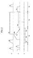
- Fig. 2 is a waveform diagram illustrating a driving waveform of the PDP according to an exemplary embodiment of the present invention.
- Fig. 3 is a waveform diagram illustrating a falling scan electrode voltage waveform and a discharge current waveform according to an exemplary embodiment of the present invention.
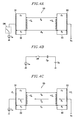
- Fig. 4A is a schematic diagram of a discharge cell formed by a sustain electrode and a scan electrode.
- Fig. 4B is a schematic diagram illustrating an equivalent circuit of Fig. 4A.
- Fig. 4C is a schematic diagram similar to that of Fig. 4A illustrating a case when no discharge occurs in the discharge cell of Fig. 4A.
- Fig. 4D is a schematic diagram similar to that of Fig. 4A illustrating a state in which a voltage is applied such that a discharge occurs in the discharge cell.
- Fig. 4E is a schematic diagram similar to that of Fig. 4A illustrating a floated state when a discharge occurs in the discharge cell.
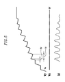
- Fig. 5 is a waveform diagram illustrating a rising waveform and a discharge current according to an exemplary embodiment of the present invention.
- Fig. 6 is a circuit diagram of a driving circuit according to a first exemplary embodiment of the present invention.
- Fig. 7 a waveform diagram illustrating a driving waveform of the driving circuit of Fig. 5.
- Figs. 8, 9, 10, 11, 12, 13, 14, 15, and 16 are circuit diagrams of driving circuits according to second, third, fourth, fifth, sixth, seventh, eighth, ninth, and tenth exemplary embodiments of the present invention, respectively.
- Fig. 1 is a schematic diagram of a PDP according to an exemplary embodiment of the present invention.
- the PDP comprises a plasma panel 100, a controller 200, an address driver 300, a sustain electrode driver (referred to as an X electrode driver hereinafter) 400, and a scan electrode driver (referred to as a Y electrode driver hereinafter) 500.
- the plasma panel 100 includes a plurality of address electrodes A 1 to A m arranged in the column direction, a plurality of sustain electrodes (referred to as X electrodes hereinafter) X 1 to X n arranged in the row direction, and a plurality of scan electrodes (referred to as Y electrodes hereinafter) Y 1 to Y n arranged in the row direction.
- the X electrodes X 1 to X n are formed corresponding to the respective Y electrodes Y 1 to Y n , and their ends are connected in common.
- the plasma panel 100 includes a glass substrate (not shown) on which the X and Y electrodes X 1 to X n and Y 1 to Y n are arranged, and a glass substrate (not shown) on which the address electrodes A 1 to A m are arranged.
- the two glass substrates face each other with a discharge space therebetween so that the Y electrodes Y 1 to Y n may cross the address electrodes A 1 to A m and the X electrodes X 1 to X n may cross the address electrodes A 1 to A m .
- discharge spaces on the crossing points of the address electrodes A 1 to A m and the X and Y electrodes X 1 to X n and Y 1 to Y n form discharge cells.
- the controller 200 externally receives video signals, and outputs address driving control signals, X electrode driving control signals, and Y electrode driving control signals. Additionally, the controller 200 divides a single frame into a plurality of subfields and drives them. Each subfield includes, sequentially, a reset period, an address period, and a sustain period.
- the address driver 300 receives address driving control signals from the controller 200, and applies display data signals to the respective address electrodes A 1 to A m for selecting desired discharge cells.
- the X electrode driver 400 receives X electrode driving control signals from the controller 200 and applies driving voltages to the X electrodes X 1 to X n .
- the Y electrode driver 500 receives Y electrode driving control signals from the controller 200, and applies driving voltages to the Y electrodes Y 1 to Y n .
- Driving waveforms applied to the address electrodes A 1 to A m , the X electrodes X 1 to X n , and the Y electrodes Y 1 to Y n for each subfield will be described with reference to Figs. 2 and 3.
- a discharge cell formed by an address electrode, an X electrode, and a Y electrode will be described below.
- Fig. 2 is a waveform diagram illustrating a driving waveform of the PDP according to one exemplary embodiment of the present invention
- Fig. 3 is a waveform diagram illustrating a falling Y electrode voltage waveform and a discharge current waveform according to an exemplary embodiment of the present invention.
- a single subfield includes a reset period P r , an address period P a , and a sustain period P s .
- the reset period P r includes an erase period P r1 , a rising period P r2 , and a falling period P r3 .
- positive charges are formed at the X electrode, and negative charges are formed at the Y electrode when the last sustaining discharge of a sustain period is finished.
- a waveform rising from a reference voltage to a voltage of V e is applied to the X electrode while the Y electrode is maintained at the reference voltage after the sustain period is finished in the erase period P r1 of the reset period P r , assuming that the reference voltage is 0V (volts).
- the charges accumulated at the X and Y electrodes are gradually erased.
- a waveform rising from a voltage of V s to a voltage of V set is applied to the Y electrode while the X electrode is maintained at 0V in the rising period P r2 of the reset period P r . Because of this, weak resetting discharges are generated between the Y electrode and the address electrode and between the X electrode and the Y electrode, and the negative charges are accumulated at the Y electrode. Positive charges are accumulated at the address electrode and the X electrode.
- a process is repeated in which the voltage applied to the Y electrode is reduced by a predetermined voltage and the Y electrode is floated by stopping the voltage applied to the Y electrode during the period of T f , while the X electrode is maintained at the voltage of V e in the falling period P r3 of the reset period P r .
- Fig. 3 also shows the firing period T r , during which voltage is applied to the Y electrode.
- the interval voltage of the discharge space is rapidly reduced by the wall charges formed on the X and Y electrodes so that an intense discharge quenching occurs in the discharge space.
- the wall charges are reduced and intense discharge quenching occurs within the discharge space.
- the exemplary embodiment quenches the discharge with a much smaller amount of wall charges to allow precise control over the wall charges, as compared with the prior art.
- the conventional reset method of applying a ramp voltage slowly increases the voltage applied to the discharge space with a constant voltage variation to prevent an intense discharge and control the wall charge.
- This conventional method of using the ramp voltage controls the intensity of the discharge using the slope of the ramp voltage and restricts the slope of the ramp to certain acceptable slope values in order to control the wall charges properly. Often, the restricted number of acceptable slope values causes the reset operation to take too long, because the ramping operation takes too long to complete.
- a reset method using a floating state T f controls the intensity of the discharge using a voltage drop based on the wall charges, thereby reducing the time required to complete the reset period.
- the falling time of the Y electrode voltage in embodiments of the invention is generally not long because an excessively intense discharge may occur if the voltage-applying time of the Y electrode is long.
- Fig. 4A is a schematic diagram of a discharge cell formed by a sustain electrode and a scan electrode.
- Fig. 4B is a schematic diagram of an equivalent circuit of Fig. 4A.
- Fig. 4C is a schematic diagram similar to that of Fig. 4A, illustrating a case when no discharge occurs in the cell.
- Fig. 4D is a schematic diagram similar to that of Fig. 4A, illustrating a state in which a voltage is applied when a discharge occurs in the discharge cell.
- Fig. 4E is a schematic diagram similar to that of Fig. 4A, illustrating a floated state when a discharge occurs in the discharge cell of Fig. 4A.
- charges - ⁇ w and + ⁇ w are formed at the Y and X electrodes 10 and 20, respectively, in an earlier stage than that depicted in Fig. 4A.
- the charges are formed on a dielectric layer of an electrode, but for ease of explanation, the charges will be described as having been formed on the electrodes.
- the Y electrode 10 is connected to a current source I in through a switch SW, and the X electrode 20 is connected to the voltage of V e .
- Dielectric layers 30 and 40 are respectively formed within the Y and X electrodes 10 and 20. Discharge gas (not shown) is injected between the dielectric layers 30 and 40, and the area provided between the dielectric layers 30 and 40 forms a discharge space 50.
- the Y and X electrodes 10 and 20, the dielectric layers 30 and 40, and the discharge space 50 form a capacitive load, they may be represented for purposes of description as a panel capacitor Cp, as shown in Fig. 4B.
- the panel capacitor Cp is defined such that the dielectric constant of the dielectric layers 30 and 40 is ⁇ r , a voltage at the discharge space 50 is V g , the thickness of the dielectric layers 30 and 40 is the same as d 1 , and the distance (the width of the discharge space) between the dielectric layers 30 and 40 is d 2 .
- the voltage V g applied to the discharge space 50 when no discharge occurs while the switch SW is turned on is calculated, assuming that the voltage applied to the Y electrode 10 is V in .
- Equation (2) ⁇ l ⁇ r ⁇ 0 ⁇ in which ⁇ t represents the charges applied to the Y and X electrodes, and ⁇ 0 is the permittivity within the discharge space.
- E 2 ⁇ l + ⁇ w ⁇ 0
- Equation (4) The voltage of (V e -V in ) applied outside the discharge cell is given by Equation (4), which describes the relationship between the electric field and the distance, and the voltage of V g of the discharge space 50 is given by Equation 5.
- Equations (2) to (5) the charges ⁇ t applied to the X or Y electrode 10 or 20 and the voltage V g within the discharge space 50 are given by Equations (6) and (7).
- V w is a voltage formed by the wall charges ⁇ w in the discharge space 50.
- the voltage V g1 within the discharge space 50 is calculated for the state in which the wall charges formed at the Y and X electrodes 10 and 20 are quenched by the amount of ⁇ w ' because of the discharge caused by the externally applied voltage of (V e -V in ).
- the charges applied to the Y and X electrodes 10 and 20 are increased to ⁇ t ' since the charges are supplied from the power V in so as to maintain the potential of the electrodes when the wall charges are formed.
- Equation (8) ⁇ t ' ⁇ r ⁇ 0
- E 2 ⁇ t ' + ⁇ w - ⁇ w ' ⁇ 0
- Equations (10) and (11) the charges ⁇ t ' applied to the Y and X electrodes 10 and 20 and the voltage V g1 within the discharge space are given by Equations (10) and (11).
- the voltage V g2 within the discharge space 50 is calculated for the state in which the switch SW is turned off (i.e., the discharge space 50 is floated) after the wall charges formed at the Y and X electrodes 10 and 20 are quenched by the amount of ⁇ w ' because of the discharge caused by the externally applied voltage V in . Since no external charges are applied, the charges applied to the Y and X electrodes 10 and 20 become ⁇ t in the same manner as described with respect to Fig. 4C.
- the electric field E 1 within the dielectric layers 30 and 40 and the electric field E 2 within the discharge space 50 are given by Equations (2) and (12).
- E 2 ⁇ t + ⁇ w - ⁇ w' ⁇ 0
- V g2 of the discharge space 50 is given by Equation (13).
- Equation (13) It is known from Equation (13) that a large voltage fall is generated by the quenched wall charges when the switch SW is turned off (floated). That is, as known from Equations (12) and (13), the voltage falling intensity caused by the wall charges in the floated state of the electrode becomes larger by a multiple of 1/(1- ⁇ ) times that of the voltage applying state. As a result, since the voltage within the discharge space 50 is substantially reduced in the floated state when a small amount of charges are reduced, the voltage between the electrodes becomes below the discharge firing voltage, and the discharge is steeply quenched. That is, floating the electrode after the discharge begins serves as an intense discharge quenching mechanism. When the voltage within the discharge space 50 is reduced, the voltage V y at the floated Y electrode is increased by a predetermined voltage, as shown in Fig. 3, since the X electrode is fixed at the voltage of V e .
- Fig. 5 illustrates a rising waveform with a firing period T r and a floating period T f .
- a process according to the present invention may include raising the Y electrode voltage by a predetermined voltage during a firing period T r and floating the Y electrode by stopping the voltage applied to the Y electrode during the floating period T f in the rising period P r2 of the reset period P r .
- a number of exemplary driving circuits for generating a falling waveform similar or identical to that shown in Fig. 3 will be described. These driving circuits may be provided in the Y electrode driver 500 and may provide the Y waveform shown in Fig. 2.
- Fig. 6 is a circuit diagram illustrating a driving circuit according to a first exemplary embodiment of the present invention
- Fig. 7 shows a driving waveform diagram of the driving circuit of Fig. 6.
- Figs. 8 and 9 are circuit diagrams of driving circuits according to second and third exemplary embodiments of the present invention, respectively.
- the panel capacitor Cp shown in Figs. 6, 8, and 9 represents the capacitive load between the Y and X electrode, as it does in Fig. 4A. It is assumed that a ground voltage is applied to a second end of the panel capacitor Cp (i.e., the X electrode), and that the panel capacitor Cp is charged with a predetermined amount of charges.
- a driving circuit includes a transistor M1, a capacitor Cd, a resistor R1, diodes D1 and D2, and a control signal voltage source Vg.
- a drain, which is one of two main ends of the transistor M1 is connected to a first end of the panel capacitor Cp, and a source, which is the other main end of the transistor M1, is connected to a first end of the capacitor Cd.
- a second end of the capacitor Cd is connected to the ground 0.
- the control signal voltage source Vg is connected between a gate, which is the control end of the transistor M1, and the ground 0, and supplies a control signal Sg to the transistor M1.
- the diode D1 and the resistor R1 are connected between the first end of the capacitor Cd and the control signal voltage source Vg, and form a discharging path allowing the capacitor Cd to be discharged.
- the diode D2 is connected between the ground 0 and the gate of the transistor M1, and clamps the gate voltage of the transistor M1.
- a resistor (not shown) may optionally be connected between the control signal voltage source Vg and the transistor M1, and a resistor (not shown) may be also connected between the gate of the transistor M1 and the ground 0.
- the transistor M1 is depicted as an n channel MOSFET, but any other switching element performing similar functions can be used instead of the n channel MOSFET.
- control signal Sg supplied by the control signal voltage source Vg alternately has a high level voltage for turning on the transistor M1, and a low level voltage for turning off the transistor M1.
- the control signal Sg becomes a high level voltage appropriate to turn on the transistor M1
- the charges accumulated in the panel capacitor Cp are moved to the capacitor Cd.
- the capacitor Cd is charged, the first end voltage of the capacitor Cd rises so that the source voltage of the transistor M1 rises.
- the gate voltage of the transistor M1 is maintained at the voltage at the time of turning on the transistor M1, but the first end voltage of the capacitor Cd rises. Therefore, the source voltage of the transistor M1 rises as compared to the gate voltage of the transistor M1.
- the gate-source voltage When the source voltage of the transistor M1 rises to a predetermined voltage, the voltage between the gate and the source (referred to as the gate-source voltage hereinafter) of the transistor M1 is lower than the threshold voltage V t of the transistor M1 so that the transistor M1 is turned off.
- the transistor M1 is turned off when the difference between the high level voltage of the control signal Sg and the source voltage of the transistor M1 is lower than the threshold voltage V t of the transistor M1.
- the transistor M1 is turned off, the voltage applied to the panel capacitor Cp is stopped so that the panel capacitor Cp is floated.
- the amount of charges ⁇ Q i charged in the capacitor Cd is given by Equation (14) when the transistor M1 is turned off.
- ⁇ Q i C d ( V cc - V t ) in which V cc is the high level voltage of the control signal Sg, and C d is the capacitance of the capacitor Cd.
- the voltage of the panel capacitor Cp is immediately reduced by the predetermined voltage because the charges are immediately moved from the panel capacitor Cp to the capacitor Cd. Therefore, the panel capacitor Cp can be floated faster than the case in which the panel capacitor is floated by controlling the level of the control signal Sg. Furthermore, the floating period T f can be longer than the voltage applying period since the transistor M1 is still turned off when the control signal Sg is at the low level.
- Equation (15) The voltage variation ⁇ V pi of the panel capacitor Cp is given by Equation (15) since the charges ⁇ Q i charged in the capacitor Cd are supplied from the panel capacitor Cp.
- Equation (17) the amount of charges ⁇ Q d discharged from the capacitor Cd is given by Equation (17) in terms of the low level time T off of the control signal Sg.
- the amount of charges Q d remaining in the capacitor Cd is given as Equation (18).
- Q d ⁇ Q i - ⁇ Q d
- the voltage of the panel capacitor Cp rises so that the transistor M1 is turned off.
- the control signal Sg becomes the low level voltage
- the capacitor Cd is discharged, and the transistor M1 remains in the turned-off state. Therefore, the voltage of the panel capacitor Cp is once again reduced in response to the high level of the control signal Sg and the panel capacitor Cp is once again floated in response to the rising of voltage of the capacitor Cd.
- the driving circuit shown in Fig. 6 is used to the plasma panel 100 where the capacitance C p of the panel capacitor Cp is about 0.1 ⁇ F.
- the voltage of the panel capacitor Cp may be reduced by 220V during about 100 ⁇ s (Pr3).
- a discharge path is formed in order to facilitate repeatedly reducing the voltage of the electrode and floating the electrode, but the discharge path can be removed if reducing the voltage of the electrode and floating the electrode are only performed once.
- the discharge path may not be connected to the positive polarity terminal of the control signal voltage source Vg but may instead be formed by a different path.
- a switching element is connected between the first end of the capacitor Cd and the ground 0, and the switching element is turned on so as to form the discharge path.
- the amount of voltage reduction in the panel capacitor C1 is controlled by controlling the duty ratio of the control signal Sg, since the reduced voltage of the panel capacitor Cp is determined by the resistor R1 and the low level period T off of the control signal Sg.
- the amount of the reduced voltage of the panel capacitor Cp is controlled by the resistance of the variable resistor R2 connected to the resistor R1 in parallel.
- the variable resistor R2 may be connected instead of the resistor R1.
- a resistor R3 is connected between the panel capacitor Cp and the transistor M1 so as to restrict the current discharged from the panel capacitor Cp.
- any other element which can restrict the current discharged from the panel capacitor Cp for example, an inductor (not shown), can be used instead of the resistor R3.
- the level of the reduced voltage decreases at the end region of the falling waveform shown in Fig. 3 so that the voltage of the panel capacitor Cp may not be reduced to the desired voltage during the given time.
- a driving circuit according to the exemplary embodiment which can shorten the time in the end region of the falling waveform will be described with reference to Fig. 10.
- Fig. 10 is a circuit diagram of a driving circuit according to a fourth exemplary embodiment of the present invention.
- the driving circuit according to the fourth exemplary embodiment further includes a transistor Q1 different from that of the first exemplary embodiment.
- the collector, which is a first end of the transistor Q1 is connected to the first end of the capacitor Cd, and the emitter, which is a second end of the transistor Q1, is connected to the ground 0. That is, the transistor Q is connected to the capacitor Cd in parallel.
- the transistor Q1 is depicted as an npn type bipolar transistor but a pnp type bipolar transistor may be used as the transistor Q1.
- any other switching elements performing similar functions can be used instead of the transistor Q1.
- the operation of the driving circuit shown in Fig. 10 is same as that of the driving circuit shown in Fig. 6 during the early stage. That is, the transistor Q1 is turned off during the early stage.
- the signal for turning on the transistor is applied to the base, which is the control end of the transistor Q1.
- the transistor Q1 is turned on so that the voltage of the capacitor Cd is discharged to the ground 0 through the transistor Q1.
- the voltage of the panel capacitor Cp is steeply reduced to the desired voltage since the voltage charged in the panel capacitor Cp is discharged through the turned on transistor Q1.
- a resistor R4 may be connected between the first end of the capacitor Cd and the first end of the transistor Q1 and/or between the second end of the transistor Q1 and the ground 0. Then, the voltage of the panel capacitor Cp is not steeply reduced when turning on the transistor Q1, but is reduced according to a time constant which is determined by the parallel connection of the resistor R4 and the capacitor Cd.
- the transistor Q1 may be turned on a predetermined length of time after the control signal Sg is applied to the transistor M1.
- transistor Q1 described in Fig. 10 may be used in the driving circuits shown in Figs. 8 and 9.
- the current flowing from the first end of the capacitor Cd to its second end is controlled by the gate-source voltage of the transistor M1 since the transistor M1 is turned off when the capacitor Cd is charged to the predetermined voltage.
- the body diode is formed in the transistor M1 in a direction from the source to the drain, as shown in Fig. 11, when the MOSFET is used as the transistor M1, the current may flow from the second end of the capacitor Cd to its first end when the voltage of the panel capacitor Cp is lower than voltage of the voltage source to which the capacitor Cd is connected (the voltage source is ground 0 in Figs. 6, 8, 9, and 10).
- the capacitor Cd may be charged continuously because there is no means for controlling this current in the driving circuits shown in Figs. 6, 8, 9, and 10. Then, the second end voltage of the capacitor Cd is higher than the first end voltage of the capacitor Cd by an amount equal to the voltage charged in the capacitor Cd, so that the gate voltage of the transistor M1 is higher than the first end voltage of the capacitor Cd (i.e., the source voltage of the transistor M1 caused by the voltage charged in the capacitor Cd). As a result, the gate-source voltage of the transistor M1 rises by the voltage charged in the capacitor Cd, and the transistor M1 may be damaged if this voltage is higher than the voltage that the transistor M1 can withstand.
- a driving circuit which can prevent the transistor M1 from being damaged by the current flowing from the second end of the capacitor Cd to the first end of it, will be described with reference to Figs. 11 and 12.
- Figs. 11 and 12 are circuit diagrams of the driving circuits according to fifth and sixth exemplary embodiments of the present invention, respectively.
- the driving circuit according to the fifth exemplary embodiment further includes a diode D3 connected to the capacitor Cd in parallel differently from the driving circuit according to the first exemplary embodiment shown in Fig. 6.
- the anode of the diode D3 is connected to the second end of the capacitor Cd
- the cathode of the diode D3 is connected to the first end of the capacitor Cd.
- the driving circuit according to the sixth exemplary embodiment further includes a diode D4 connected between the capacitor Cd and the transistor M1 differently from the driving circuit according to the first exemplary embodiment shown in Fig. 6.
- the anode of the diode D4 is connected to the first end of the panel capacitor Cp
- the cathode of the diode D4 is connected to the drain of the transistor M1. Then, the current which can be generated by the body diode of the transistor M1 is intercepted since the diode is formed in the opposite direction of the body diode of the transistor M1.
- the diode D4 is connected between the panel capacitor Cp and the transistor M1, but the diode D4 may be formed in any position of the path including the panel capacitor Cp, the transistor M1, and the capacitor Cd.
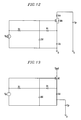
- Figs. 13 to 16 are circuit diagrams of driving circuits according to seventh to tenth exemplary embodiments of the present invention, respectively. Since the configurations and the operations of the circuits of Figs. 13 to 16 are similar to those of Figs. 6, 10, 11, and 12, respectively, only differences between the circuits of Figs. 6, 10, 11, and 12 and those of Figs. 13 to 16 will be described, and the same portions or those which are readily apparent from Figs. 6, 10, 11, and 12 will be omitted.
- the drain of the transistor M1 is connected to the voltage source supplying the high voltage V set .
- the capacitor Cd is connected between the source of the transistor M1 and the first end of the panel capacitor Cp (i.e., the Y electrode).
- the transistor M1 is turned on, the capacitor Cd and the panel capacitor Cp are charged by the V set voltage.
- the transistor M1 is turned off when the voltage of the capacitor Cd increases to a predetermined voltage.
- the driving circuit according to the eighth exemplary embodiment further includes a transistor Q1.
- the first end of the transistor Q1 is connected to the first end of the capacitor CD, and the second end of the transistor Q1 is connected to the panel capacitor Cp. That is, the transistor Q1 is connected to the capacitor Cd.
- the voltage of the panel capacitor Cp steeply increases to the desired voltage within the given time since the V set voltage is applied to the panel capacitor through the transistors M1 and Q1 when the transistors Q1 and M1 are turned on.
- the resistor R4 may be connected between the first end of the capacitor Cd and the first end of the transistor Q1 and/or between the second end of the transistor Q1 and the panel capacitor Cp as described in Fig. 10. Then, the voltage of the panel capacitor Cp is reduced according to the time constant, which is determined by the parallel connection of the capacitor Cd and the resistor R4.
- the current may flow from the second end of the capacitor Cd to its first end by the body diode of the transistor M1 so that the transistor may be damaged. Therefore, the diode D3 or D4 described in Fig. 11 or 12 may be included in the driving circuit of Fig. 13. This exemplary embodiment will be described with reference to Figs. 15 and 16.
- the driving circuit according to the ninth exemplary embodiment further includes a diode D3.
- the anode of the diode D3 is connected to the second end of the capacitor Cd, and the cathode of the diode D3 is connected to the first end of the capacitor Cd. Consequently, the current generated by the body diode of the transistor M1 flows through the diode D3 so that the capacitor Cd is not charged by this current. As a result, the gate-source voltage of the transistor M1 is never higher than the voltage that the transistor M1 can withstand.
- the driving circuit according to the tenth exemplary embodiment further includes a diode D4.
- the anode of the diode D4 is connected to the second end of the capacitor Cd, and the cathode of the diode D3 is connected to the first end of the panel capacitor Cp. Consequently, the current that is generated by the body diode of the transistor M1 is intercepted by the diode D4, which is formed in the opposite direction of the body diode of the transistor M1.
- the diode D4 may be formed in any position of the path including the voltage source supplying V set voltage, the transistor M1, the capacitor Cd, and the panel capacitor Cp.
- Embodiments of the present invention provide a driving circuit for repeatedly floating the electrode after making the voltage applied to the electrode rise or fall. Additionally, in embodiments of the invention, the wall charges formed at the discharge cell are precisely controlled by the floating operation.
Landscapes
- Engineering & Computer Science (AREA)
- Physics & Mathematics (AREA)
- Power Engineering (AREA)
- Plasma & Fusion (AREA)
- Computer Hardware Design (AREA)
- General Physics & Mathematics (AREA)
- Theoretical Computer Science (AREA)
- Control Of Indicators Other Than Cathode Ray Tubes (AREA)
- Control Of Gas Discharge Display Tubes (AREA)
Applications Claiming Priority (6)
| Application Number | Priority Date | Filing Date | Title |
|---|---|---|---|
| KR2003040688 | 2003-06-23 | ||
| KR10-2003-0040688A KR100477974B1 (ko) | 2003-06-23 | 2003-06-23 | 플라즈마 디스플레이 패널의 구동 장치 및 구동 방법 |
| KR2003070247 | 2003-10-09 | ||
| KR10-2003-0070247A KR100497239B1 (ko) | 2003-10-09 | 2003-10-09 | 플라즈마 디스플레이 패널의 구동 장치 |
| KR2003071757 | 2003-10-15 | ||
| KR10-2003-0071757A KR100502900B1 (ko) | 2003-10-15 | 2003-10-15 | 플라즈마 디스플레이 패널의 구동 장치 |
Publications (3)
| Publication Number | Publication Date |
|---|---|
| EP1492076A2 true EP1492076A2 (de) | 2004-12-29 |
| EP1492076A3 EP1492076A3 (de) | 2008-03-05 |
| EP1492076B1 EP1492076B1 (de) | 2011-11-16 |
Family
ID=33424826
Family Applications (1)
| Application Number | Title | Priority Date | Filing Date |
|---|---|---|---|
| EP04090250A Expired - Lifetime EP1492076B1 (de) | 2003-06-23 | 2004-06-22 | Ansteuerschaltung und Verfahren für eine Plasmaanzeigetafel |
Country Status (4)
| Country | Link |
|---|---|
| US (1) | US7737921B2 (de) |
| EP (1) | EP1492076B1 (de) |
| JP (1) | JP5009492B2 (de) |
| CN (1) | CN100377190C (de) |
Cited By (1)
| Publication number | Priority date | Publication date | Assignee | Title |
|---|---|---|---|---|
| EP2023323A3 (de) * | 2007-08-08 | 2009-09-30 | Samsung SDI Co., Ltd. | Plasmaanzeigevorrichtung und Verfahren zu ihrer Ansteuerung |
Families Citing this family (5)
| Publication number | Priority date | Publication date | Assignee | Title |
|---|---|---|---|---|
| KR100508942B1 (ko) | 2004-03-11 | 2005-08-17 | 삼성에스디아이 주식회사 | 플라즈마 표시 패널의 구동 장치 |
| KR100515327B1 (ko) * | 2004-04-12 | 2005-09-15 | 삼성에스디아이 주식회사 | 플라즈마 표시 패널의 구동 방법 및 플라즈마 표시 장치 |
| KR100578933B1 (ko) * | 2005-01-25 | 2006-05-11 | 삼성에스디아이 주식회사 | 플라즈마 표시 장치와 플라즈마 표시 패널의 구동 장치 및구동 방법 |
| KR100713278B1 (ko) * | 2005-11-15 | 2007-05-04 | 엘지전자 주식회사 | 영상표시기기의 전원 제어장치 |
| US8096264B2 (en) | 2007-11-30 | 2012-01-17 | Illinois Tool Works Inc. | Repulsion ring |
Family Cites Families (16)
| Publication number | Priority date | Publication date | Assignee | Title |
|---|---|---|---|---|
| FR2547131B1 (fr) * | 1983-03-18 | 1985-10-11 | France Etat Armement | Amplificateur haute tension pour charge capacitive |
| JPH0766247B2 (ja) * | 1990-07-06 | 1995-07-19 | 富士ゼロックス株式会社 | El駆動回路 |
| US5745086A (en) | 1995-11-29 | 1998-04-28 | Plasmaco Inc. | Plasma panel exhibiting enhanced contrast |
| EP1202241B1 (de) * | 1998-09-04 | 2007-09-12 | Matsushita Electric Industrial Co., Ltd. | Verfahren und Einrichtung zum Steuern eines Plasmabildschirms mit höherer Bildqualität und hohem Leuchtwirkungsgrad |
| JP3455141B2 (ja) * | 1999-06-29 | 2003-10-14 | 富士通株式会社 | プラズマディスプレイパネルの駆動方法 |
| JP2001013912A (ja) * | 1999-06-30 | 2001-01-19 | Fujitsu Ltd | 容量性負荷の駆動方法及び駆動回路 |
| KR100598182B1 (ko) * | 1999-07-23 | 2006-07-10 | 엘지전자 주식회사 | 플라즈마 디스플레이 패널 및 이 패널의 구동 방법과 장치 |
| US7053869B2 (en) * | 2000-02-24 | 2006-05-30 | Lg Electronics Inc. | PDP energy recovery apparatus and method and high speed addressing method using the same |
| JP2002132208A (ja) * | 2000-10-27 | 2002-05-09 | Fujitsu Ltd | プラズマディスプレイパネルの駆動方法および駆動回路 |
| JP4149263B2 (ja) | 2001-01-18 | 2008-09-10 | エルジー エレクトロニクス インコーポレーテッド | プラズマディスプレイパネル及びその駆動方法 |
| KR100450179B1 (ko) * | 2001-09-11 | 2004-09-24 | 삼성에스디아이 주식회사 | 플라즈마 디스플레이 패널의 구동 방법 |
| FR2840468B1 (fr) * | 2002-05-28 | 2004-08-27 | St Microelectronics Sa | Dispositif amplificateur inverseur haute tension |
| US7009823B2 (en) * | 2002-06-28 | 2006-03-07 | Lg Electronics Inc. | Energy recovery circuit and energy recovery method using the same |
| KR100472353B1 (ko) * | 2002-08-06 | 2005-02-21 | 엘지전자 주식회사 | 플라즈마 디스플레이 패널의 구동장치 및 구동방법 |
| KR100484647B1 (ko) * | 2002-11-11 | 2005-04-20 | 삼성에스디아이 주식회사 | 플라즈마 디스플레이 패널의 구동장치 및 구동방법 |
| KR100490631B1 (ko) * | 2003-05-14 | 2005-05-17 | 삼성에스디아이 주식회사 | 플라즈마 디스플레이 패널 및 이의 구동방법 |
-
2004
- 2004-05-28 JP JP2004159647A patent/JP5009492B2/ja not_active Expired - Fee Related
- 2004-06-22 EP EP04090250A patent/EP1492076B1/de not_active Expired - Lifetime
- 2004-06-23 US US10/873,649 patent/US7737921B2/en not_active Expired - Fee Related
- 2004-06-23 CN CNB2004100714968A patent/CN100377190C/zh not_active Expired - Fee Related
Non-Patent Citations (1)
| Title |
|---|
| None |
Cited By (2)
| Publication number | Priority date | Publication date | Assignee | Title |
|---|---|---|---|---|
| EP2023323A3 (de) * | 2007-08-08 | 2009-09-30 | Samsung SDI Co., Ltd. | Plasmaanzeigevorrichtung und Verfahren zu ihrer Ansteuerung |
| US8203508B2 (en) | 2007-08-08 | 2012-06-19 | Samsung Sdi Co., Ltd. | Plasma display device and driving method thereof |
Also Published As
| Publication number | Publication date |
|---|---|
| JP2005018045A (ja) | 2005-01-20 |
| EP1492076B1 (de) | 2011-11-16 |
| US7737921B2 (en) | 2010-06-15 |
| JP5009492B2 (ja) | 2012-08-22 |
| EP1492076A3 (de) | 2008-03-05 |
| US20050030260A1 (en) | 2005-02-10 |
| CN1573867A (zh) | 2005-02-02 |
| CN100377190C (zh) | 2008-03-26 |
Similar Documents
| Publication | Publication Date | Title |
|---|---|---|
| CN100410986C (zh) | 等离子显示面板及其驱动方法 | |
| US7365709B2 (en) | Plasma display panel driver | |
| EP1492076B1 (de) | Ansteuerschaltung und Verfahren für eine Plasmaanzeigetafel | |
| US20050083259A1 (en) | Driving device and method of plasma display panel | |
| US20050073480A1 (en) | Plasma display panel and driving method thereof | |
| US20060164336A1 (en) | Plasma display, driving device and method of operating the same | |
| US20050083262A1 (en) | Plasma display panel driving device and method | |
| US7542020B2 (en) | Power supply device and plasma display device including power supply device | |
| US7460089B2 (en) | Driving apparatus of plasma display panel | |
| KR100831015B1 (ko) | 플라즈마 표시 장치 및 그 구동 방법 | |
| US20060061523A1 (en) | Plasma display device and driving method thereof | |
| US7652639B2 (en) | Driving method of plasma display panel and plasma display | |
| KR100477974B1 (ko) | 플라즈마 디스플레이 패널의 구동 장치 및 구동 방법 | |
| KR100502900B1 (ko) | 플라즈마 디스플레이 패널의 구동 장치 | |
| US20080272704A1 (en) | Plasma display and driving method thereof | |
| US20090128526A1 (en) | Plasma display device and driving apparatus thereof | |
| KR100497239B1 (ko) | 플라즈마 디스플레이 패널의 구동 장치 | |
| KR100502899B1 (ko) | 플라즈마 디스플레이 패널의 구동 장치 | |
| KR100497237B1 (ko) | 플라즈마 디스플레이 패널의 구동 장치 및 구동 방법 | |
| US20080174525A1 (en) | Plasma display device and voltage generator thereof | |
| US20080266280A1 (en) | Plasma display and control method thereof | |
| US20090040210A1 (en) | Scan electrode driver for a plasma display | |
| KR20080034063A (ko) | 플라즈마 표시 장치 및 그 구동 방법 |
Legal Events
| Date | Code | Title | Description |
|---|---|---|---|
| PUAI | Public reference made under article 153(3) epc to a published international application that has entered the european phase |
Free format text: ORIGINAL CODE: 0009012 |
|
| 17P | Request for examination filed |
Effective date: 20040622 |
|
| AK | Designated contracting states |
Kind code of ref document: A2 Designated state(s): AT BE BG CH CY CZ DE DK EE ES FI FR GB GR HU IE IT LI LU MC NL PL PT RO SE SI SK TR |
|
| AX | Request for extension of the european patent |
Extension state: AL HR LT LV MK |
|
| RIN1 | Information on inventor provided before grant (corrected) |
Inventor name: KIM, JIN-SUNG Inventor name: LEE, DONG-YOUNG Inventor name: KIM, TAE-SEONG Inventor name: CHAE, SEUNG-HUN,CHEONGMYUNG MAEUL Inventor name: CHUNG, WOO-JOON,SAMSUNG SDI DORMITORY Inventor name: KANG, KYOUNG-HO,SINNAMUSIL SINSUNG |
|
| PUAL | Search report despatched |
Free format text: ORIGINAL CODE: 0009013 |
|
| AK | Designated contracting states |
Kind code of ref document: A3 Designated state(s): AT BE BG CH CY CZ DE DK EE ES FI FR GB GR HU IE IT LI LU MC NL PL PT RO SE SI SK TR |
|
| AX | Request for extension of the european patent |
Extension state: AL HR LT LV MK |
|
| 17Q | First examination report despatched |
Effective date: 20080507 |
|
| AKX | Designation fees paid |
Designated state(s): DE FR GB NL |
|
| GRAP | Despatch of communication of intention to grant a patent |
Free format text: ORIGINAL CODE: EPIDOSNIGR1 |
|
| GRAS | Grant fee paid |
Free format text: ORIGINAL CODE: EPIDOSNIGR3 |
|
| GRAA | (expected) grant |
Free format text: ORIGINAL CODE: 0009210 |
|
| AK | Designated contracting states |
Kind code of ref document: B1 Designated state(s): DE FR GB NL |
|
| REG | Reference to a national code |
Ref country code: GB Ref legal event code: FG4D |
|
| REG | Reference to a national code |
Ref country code: DE Ref legal event code: R096 Ref document number: 602004035297 Country of ref document: DE Effective date: 20120126 |
|
| REG | Reference to a national code |
Ref country code: NL Ref legal event code: VDEP Effective date: 20111116 |
|
| PG25 | Lapsed in a contracting state [announced via postgrant information from national office to epo] |
Ref country code: NL Free format text: LAPSE BECAUSE OF FAILURE TO SUBMIT A TRANSLATION OF THE DESCRIPTION OR TO PAY THE FEE WITHIN THE PRESCRIBED TIME-LIMIT Effective date: 20111116 |
|
| REG | Reference to a national code |
Ref country code: DE Ref legal event code: R083 Ref document number: 602004035297 Country of ref document: DE |
|
| PLBE | No opposition filed within time limit |
Free format text: ORIGINAL CODE: 0009261 |
|
| STAA | Information on the status of an ep patent application or granted ep patent |
Free format text: STATUS: NO OPPOSITION FILED WITHIN TIME LIMIT |
|
| 26N | No opposition filed |
Effective date: 20120817 |
|
| REG | Reference to a national code |
Ref country code: DE Ref legal event code: R097 Ref document number: 602004035297 Country of ref document: DE Effective date: 20120817 |
|
| PGFP | Annual fee paid to national office [announced via postgrant information from national office to epo] |
Ref country code: GB Payment date: 20130530 Year of fee payment: 10 Ref country code: DE Payment date: 20130524 Year of fee payment: 10 |
|
| PGFP | Annual fee paid to national office [announced via postgrant information from national office to epo] |
Ref country code: FR Payment date: 20130606 Year of fee payment: 10 |
|
| REG | Reference to a national code |
Ref country code: DE Ref legal event code: R119 Ref document number: 602004035297 Country of ref document: DE |
|
| GBPC | Gb: european patent ceased through non-payment of renewal fee |
Effective date: 20140622 |
|
| REG | Reference to a national code |
Ref country code: FR Ref legal event code: ST Effective date: 20150227 |
|
| PG25 | Lapsed in a contracting state [announced via postgrant information from national office to epo] |
Ref country code: DE Free format text: LAPSE BECAUSE OF NON-PAYMENT OF DUE FEES Effective date: 20150101 |
|
| REG | Reference to a national code |
Ref country code: DE Ref legal event code: R119 Ref document number: 602004035297 Country of ref document: DE Effective date: 20150101 |
|
| PG25 | Lapsed in a contracting state [announced via postgrant information from national office to epo] |
Ref country code: GB Free format text: LAPSE BECAUSE OF NON-PAYMENT OF DUE FEES Effective date: 20140622 Ref country code: FR Free format text: LAPSE BECAUSE OF NON-PAYMENT OF DUE FEES Effective date: 20140630 |