EP1492162A2 - Methode zur Herstellung einer Nickelsilizidschicht - Google Patents
Methode zur Herstellung einer Nickelsilizidschicht Download PDFInfo
- Publication number
- EP1492162A2 EP1492162A2 EP03027922A EP03027922A EP1492162A2 EP 1492162 A2 EP1492162 A2 EP 1492162A2 EP 03027922 A EP03027922 A EP 03027922A EP 03027922 A EP03027922 A EP 03027922A EP 1492162 A2 EP1492162 A2 EP 1492162A2
- Authority
- EP
- European Patent Office
- Prior art keywords
- nickel
- layer
- forming
- nickel silicide
- silicide
- Prior art date
- Legal status (The legal status is an assumption and is not a legal conclusion. Google has not performed a legal analysis and makes no representation as to the accuracy of the status listed.)
- Withdrawn
Links
Images


Classifications
-
- H—ELECTRICITY
- H10—SEMICONDUCTOR DEVICES; ELECTRIC SOLID-STATE DEVICES NOT OTHERWISE PROVIDED FOR
- H10D—INORGANIC ELECTRIC SEMICONDUCTOR DEVICES
- H10D30/00—Field-effect transistors [FET]
- H10D30/01—Manufacture or treatment
- H10D30/021—Manufacture or treatment of FETs having insulated gates [IGFET]
- H10D30/0212—Manufacture or treatment of FETs having insulated gates [IGFET] using self-aligned silicidation
-
- H—ELECTRICITY
- H10—SEMICONDUCTOR DEVICES; ELECTRIC SOLID-STATE DEVICES NOT OTHERWISE PROVIDED FOR
- H10P—GENERIC PROCESSES OR APPARATUS FOR THE MANUFACTURE OR TREATMENT OF DEVICES COVERED BY CLASS H10
- H10P95/00—Generic processes or apparatus for manufacture or treatments not covered by the other groups of this subclass
- H10P95/50—Alloying conductive materials with semiconductor bodies
-
- H—ELECTRICITY
- H10—SEMICONDUCTOR DEVICES; ELECTRIC SOLID-STATE DEVICES NOT OTHERWISE PROVIDED FOR
- H10D—INORGANIC ELECTRIC SEMICONDUCTOR DEVICES
- H10D30/00—Field-effect transistors [FET]
- H10D30/01—Manufacture or treatment
- H10D30/021—Manufacture or treatment of FETs having insulated gates [IGFET]
- H10D30/0223—Manufacture or treatment of FETs having insulated gates [IGFET] having source and drain regions or source and drain extensions self-aligned to sides of the gate
- H10D30/0227—Manufacture or treatment of FETs having insulated gates [IGFET] having source and drain regions or source and drain extensions self-aligned to sides of the gate having both lightly-doped source and drain extensions and source and drain regions self-aligned to the sides of the gate, e.g. lightly-doped drain [LDD] MOSFET or double-diffused drain [DDD] MOSFET
-
- H—ELECTRICITY
- H10—SEMICONDUCTOR DEVICES; ELECTRIC SOLID-STATE DEVICES NOT OTHERWISE PROVIDED FOR
- H10D—INORGANIC ELECTRIC SEMICONDUCTOR DEVICES
- H10D30/00—Field-effect transistors [FET]
- H10D30/60—Insulated-gate field-effect transistors [IGFET]
- H10D30/601—Insulated-gate field-effect transistors [IGFET] having lightly-doped drain or source extensions, e.g. LDD IGFETs or DDD IGFETs
-
- H—ELECTRICITY
- H10—SEMICONDUCTOR DEVICES; ELECTRIC SOLID-STATE DEVICES NOT OTHERWISE PROVIDED FOR
- H10D—INORGANIC ELECTRIC SEMICONDUCTOR DEVICES
- H10D64/00—Electrodes of devices having potential barriers
- H10D64/01—Manufacture or treatment
- H10D64/011—Manufacture or treatment of electrodes ohmically coupled to a semiconductor
- H10D64/0111—Manufacture or treatment of electrodes ohmically coupled to a semiconductor to Group IV semiconductors
- H10D64/0112—Manufacture or treatment of electrodes ohmically coupled to a semiconductor to Group IV semiconductors using conductive layers comprising silicides
-
- H—ELECTRICITY
- H10—SEMICONDUCTOR DEVICES; ELECTRIC SOLID-STATE DEVICES NOT OTHERWISE PROVIDED FOR
- H10D—INORGANIC ELECTRIC SEMICONDUCTOR DEVICES
- H10D64/00—Electrodes of devices having potential barriers
- H10D64/01—Manufacture or treatment
- H10D64/013—Manufacture or treatment of electrodes having a conductor capacitively coupled to a semiconductor by an insulator
- H10D64/01302—Manufacture or treatment of electrodes having a conductor capacitively coupled to a semiconductor by an insulator the insulator being formed after the semiconductor body, the semiconductor being silicon
- H10D64/01304—Manufacture or treatment of electrodes having a conductor capacitively coupled to a semiconductor by an insulator the insulator being formed after the semiconductor body, the semiconductor being silicon characterised by the conductor
- H10D64/01306—Manufacture or treatment of electrodes having a conductor capacitively coupled to a semiconductor by an insulator the insulator being formed after the semiconductor body, the semiconductor being silicon characterised by the conductor the conductor comprising a layer of silicon contacting the insulator, e.g. polysilicon
- H10D64/01308—Manufacture or treatment of electrodes having a conductor capacitively coupled to a semiconductor by an insulator the insulator being formed after the semiconductor body, the semiconductor being silicon characterised by the conductor the conductor comprising a layer of silicon contacting the insulator, e.g. polysilicon the conductor further comprising a non-elemental silicon additional conductive layer, e.g. a metal silicide layer formed by the reaction of silicon with an implanted metal
- H10D64/0131—Manufacture or treatment of electrodes having a conductor capacitively coupled to a semiconductor by an insulator the insulator being formed after the semiconductor body, the semiconductor being silicon characterised by the conductor the conductor comprising a layer of silicon contacting the insulator, e.g. polysilicon the conductor further comprising a non-elemental silicon additional conductive layer, e.g. a metal silicide layer formed by the reaction of silicon with an implanted metal the additional conductive layer comprising a silicide layer formed by the silicidation reaction between the layer of silicon with a metal layer which is not formed by metal implantation
-
- H—ELECTRICITY
- H10—SEMICONDUCTOR DEVICES; ELECTRIC SOLID-STATE DEVICES NOT OTHERWISE PROVIDED FOR
- H10D—INORGANIC ELECTRIC SEMICONDUCTOR DEVICES
- H10D64/00—Electrodes of devices having potential barriers
- H10D64/01—Manufacture or treatment
- H10D64/013—Manufacture or treatment of electrodes having a conductor capacitively coupled to a semiconductor by an insulator
- H10D64/01302—Manufacture or treatment of electrodes having a conductor capacitively coupled to a semiconductor by an insulator the insulator being formed after the semiconductor body, the semiconductor being silicon
- H10D64/01304—Manufacture or treatment of electrodes having a conductor capacitively coupled to a semiconductor by an insulator the insulator being formed after the semiconductor body, the semiconductor being silicon characterised by the conductor
- H10D64/01306—Manufacture or treatment of electrodes having a conductor capacitively coupled to a semiconductor by an insulator the insulator being formed after the semiconductor body, the semiconductor being silicon characterised by the conductor the conductor comprising a layer of silicon contacting the insulator, e.g. polysilicon
- H10D64/01308—Manufacture or treatment of electrodes having a conductor capacitively coupled to a semiconductor by an insulator the insulator being formed after the semiconductor body, the semiconductor being silicon characterised by the conductor the conductor comprising a layer of silicon contacting the insulator, e.g. polysilicon the conductor further comprising a non-elemental silicon additional conductive layer, e.g. a metal silicide layer formed by the reaction of silicon with an implanted metal
- H10D64/01312—Manufacture or treatment of electrodes having a conductor capacitively coupled to a semiconductor by an insulator the insulator being formed after the semiconductor body, the semiconductor being silicon characterised by the conductor the conductor comprising a layer of silicon contacting the insulator, e.g. polysilicon the conductor further comprising a non-elemental silicon additional conductive layer, e.g. a metal silicide layer formed by the reaction of silicon with an implanted metal the additional layer comprising a metal or metal silicide formed by deposition, i.e. without a silicidation reaction, e.g. sputter deposition
-
- H—ELECTRICITY
- H10—SEMICONDUCTOR DEVICES; ELECTRIC SOLID-STATE DEVICES NOT OTHERWISE PROVIDED FOR
- H10D—INORGANIC ELECTRIC SEMICONDUCTOR DEVICES
- H10D64/00—Electrodes of devices having potential barriers
- H10D64/01—Manufacture or treatment
- H10D64/017—Manufacture or treatment using dummy gates in processes wherein at least parts of the final gates are self-aligned to the dummy gates, i.e. replacement gate processes
-
- H—ELECTRICITY
- H10—SEMICONDUCTOR DEVICES; ELECTRIC SOLID-STATE DEVICES NOT OTHERWISE PROVIDED FOR
- H10D—INORGANIC ELECTRIC SEMICONDUCTOR DEVICES
- H10D64/00—Electrodes of devices having potential barriers
- H10D64/60—Electrodes characterised by their materials
- H10D64/66—Electrodes having a conductor capacitively coupled to a semiconductor by an insulator, e.g. MIS electrodes
- H10D64/661—Electrodes having a conductor capacitively coupled to a semiconductor by an insulator, e.g. MIS electrodes the conductor comprising a layer of silicon contacting the insulator, e.g. polysilicon having vertical doping variation
- H10D64/662—Electrodes having a conductor capacitively coupled to a semiconductor by an insulator, e.g. MIS electrodes the conductor comprising a layer of silicon contacting the insulator, e.g. polysilicon having vertical doping variation the conductor further comprising additional layers, e.g. multiple silicon layers having different crystal structures
- H10D64/664—Electrodes having a conductor capacitively coupled to a semiconductor by an insulator, e.g. MIS electrodes the conductor comprising a layer of silicon contacting the insulator, e.g. polysilicon having vertical doping variation the conductor further comprising additional layers, e.g. multiple silicon layers having different crystal structures the additional layers comprising a barrier layer between the layer of silicon and an upper metal or metal silicide layer
Definitions
- the present invention relates a method of forming a nickel silicide layer on an exposed silicon surface and to a method of manufacturing a semiconductor device using such nickel silicide layer forming method.
- a number of metals including tungsten, tantalum, zirconium, titanium, hafnium, platinum, palladium, vanadium, niobium, cobalt, nickel and various alloys of such metals have been used to form silicide layers on semiconductor devices.
- metals including tungsten, tantalum, zirconium, titanium, hafnium, platinum, palladium, vanadium, niobium, cobalt, nickel and various alloys of such metals have been used to form silicide layers on semiconductor devices.
- gate lengths below about 100 nm, however, conventional salicide processes and materials tend to experience a variety of difficulties including opens, residues and layer non-uniformity, resulting at least in part from agglomeration within the silicide material layer.
- the initial stoichiometry of the silicide may be generally represented as CoSi, but as the annealing process continues, particularly at higher temperatures, the silicide tends to incorporate an increasing amount of silicon and approaches a composition more closely represented as CoSi 2 .
- the second high temperature silicidation used in conventional Co salicide processes tends to induce agglomeration within the silicide material layer, increasing the degree of non-uniformity within the layer and tending to degrade the performance of the resulting devices.
- Nickel is an attractive metal for forming silicides because the annealing process required to form the desired silicide may be conducted at a relatively low temperature, e.g ., below about 550 °C. Depending on the reaction conditions, nickel can react with silicon to form dinickel monosilicide, Ni 2 Si, nickel silicide, NiSi, or nickel disilicide, NiSi 2 , as the silicidation product. Using annealing temperatures greater than about 550 °C. tends to increase the formation of the most resistive nickel-disilicide NiSi 2 and a corresponding increase in the silicon consumption and are, therefore, generally avoided.
- Nickel silicide NiSi
- NiSi can be preferentially formed at lower temperatures and provides the lowest sheet resistance of the three nickel silicide phases. Due to the low silicidation temperature, NiSi exhibits a decreased tendency to agglomerate and form a silicide layer in which the sheet resistance is generally independent of the device dimensions, increasing its utility for lowering the resistance of fine line structures.
- the invention solves this problem by providing a nickel silicide layer forming method according to claim 1 and a semiconductor device manufacturing method according to claim 11.
- Embodiments of the present invention provide methods of forming a nickel silicide layer by the reaction between a nickel alloy and an exposed silicon surface comprising depositing a nickel alloy layer on the exposed silicon surface, the nickel alloy including nickel and an alloying metal, reacting the nickel alloy layer with the exposed silicon surface to form a nickel silicide layer having an upper layer and a lower layer, wherein the alloying metal is preferentially segregated into the upper layer.
- the lower layer and the upper layer of the silicide layer will have different compositions and different thicknesses.
- the lower layer for instance tends to be the thicker of the two layers and will typically include at least about 95 atomic percent nickel and silicon, with the nickel and silicon being present in an atomic ratio of about 1 and present primarily as NiSi with, at most, only minor amounts of NiSi 2 .
- the upper layer tends to be the thinner of the two layers and to incorporate the majority of the alloying metal, such as tantalum.
- the alloying metal such as tantalum.
- the final concentration of nickel and silicon in the upper layer can vary widely including, for example, between about 2 and about 90 atomic percent, and be present in atomic ratios between about 1:1 and about 2:1.
- Exemplary methods of forming the silicide layers may include forming a capping layer of a material such as titanium nitride, TiN, and particularly a nitrogen-rich TiN layer, i.e., a N:Ti atomic ratio of at least about 0.5 and as high as about 2, on the nickel alloy layer prior to forming the silicide.
- the alloying metal selected should exhibit both a diffusivity and a solubility in silicon that are lower than the corresponding values for nickel.
- the alloying metal should also exhibit a silicidation temperature in excess of that necessary to form nickel silicide.
- Tantalum has been identified as an alloying metal that possesses this combination of properties and appears to be useful for forming silicides according to the exemplary embodiments of the invention at concentrations of up to at least about 10 atomic percent, with levels in the range of between about 0.1 atomic percent and about 5 atomic percent, and particularly about 3.5 atomic percent exhibiting acceptable performance.
- nickel silicides according to the exemplary embodiments of the invention may be formed only on the gate electrode structure, only on the surface of active regions, e.g ., the source/drain regions of MOS transistors, or on both the gate electrode and the active regions.
- the gate electrode structure will typically include one or more capping layers to protect a polysilicon layer provided above the gate dielectric layer.
- a sequence of insulator deposition typically one or more layers of a chemical vapor deposition (CVD) oxide, can be formed on the substrate.
- the upper portion of the insulator(s) may then be removed using, for example, a chemical-mechanical polishing or etchback process, to expose an upper silicon surface on the gate electrode structure while protecting the active regions from exposure to the nickel alloy.
- a layer of a nickel alloy will be deposited on a substrate having regions with exposed silicon and/or polysilicon surfaces, typically followed by the deposition of an optional capping layer such as TiN.
- a heat treatment typically at a temperature of at least 250 °C., will be used to react the nickel alloy with the exposed silicon surfaces to form the desired silicide.
- the capping layer and the unreacted nickel alloy may then be removed to prepare the substrate for additional processing.
- the alloying metal used in conjunction with the primary nickel component may be selected from a group consisting of tantalum, vanadium, zirconium, hafnium, tungsten, cobalt, platinum, chromium, palladium, niobium and combinations thereof, but will generally constitute no more than about 10 atomic percent of the nickel alloy.
- the nickel silicide formation will typically include heating the nickel alloy in contact with a silicon surface to a temperature above about 200 °C. and below about 700 °C., more typically between about 250 °C. and about 500 °C., for a period of at least about 10 seconds and possibly 30 minutes or longer.
- the particular time and temperature combination selected should be sufficient to produce the two-layered nickel silicide structure described above in which the majority of the nickel is present in the lower layer as NiSi and the majority of the alloying metal has been segregated into the upper layer.
- the thermal activity of subsequent processes should generally be selected to maintain the majority, typically at least 90%, of the initial NiSi phase, i.e ., suppress conversion of NiSi to NiSi 2 , in the final semiconductor device.
- Nickel silicides prepared according to the exemplary embodiments of the present invention exhibit performance improvements over both nickel silicides prepared from unalloyed nickel and more conventional cobalt silicides, particularly for devices incorporating gate structures below 100 nm and more particularly for devices incorporating gate structures below 50 nm.
- nickel silicides according to the present invention tend to exhibit lower and more stable sheet resistance, both upon formation and particularly after additional thermal processing.
- devices incorporating nickel silicides according to the exemplary embodiments tend to exhibit improved threshold voltages V th , reduced diode leakage currents, improved off-current I doff and saturation current I dsat performance over the performance provided by identical devices incorporating cobalt silicides, particularly in PMOS devices.
- a high tensile tension capping layer such as, for example, a SiON layer, particularly on NMOS transistors that incorporate the exemplary nickel silicides according to the invention can further improve NMOS device performance.
- FIG. 1 illustrates certain of the process steps in an exemplary method for manufacturing semiconductor devices incorporating a nickel-alloy salicide structure in the gate region;
- FIGS. 2A-2G illustrate selected steps in the manufacture of semiconductor devices incorporating a nickel-alloy salicide structure
- FIG. 3 is an enlarged illustration of a portion of the silicide structure from FIG. 2G;
- FIG. 4 illustrates an embodiment of the invention in which silicide is formed on both the source/drain regions and the gate electrode
- FIGS. 5A-5C illustrate an embodiment of the invention in which the silicide is limited to the gate electrode structure
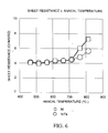
- FIG. 6 is a graph illustrating the sheet resistance of the resulting silicide layer as a function of the metal layer composition and the annealing temperature
- FIG. 7 is a graph illustrating the sheet resistance of silicide layers exposed to additional annealing as a function of the metal layer composition and the annealing temperature
- FIG. 8 is a graph illustrating the cumulative measurement of sheet resistance measured on a 50 nm gate pattern as a function of the metal layer composition and the formation temperature;
- FIG. 9 is a graph illustrating the sheet resistance of the resulting silicide as a function of the tantalum concentration.
- FIG. 10 is a TEM micrograph illustrating the formation of the two layer structure
- an exemplary method of forming a semiconductor device will include the steps of forming a gate pattern, S10, forming a lightly-doped drain (LDD) using the gate pattern as the implant mask.
- S20 forming spacer structures adjacent the sidewalls of the gate pattern, S30, forming the source/drain regions using the gate pattern and the spacer structures as the implant mask, S40, sequentially depositing a nickel alloy and a titanium nitride layer, S50, performing a thermal silicidation process to cause the nickel alloy to form a silicide, S60, forming an interlayer dielectric (ILD), S70, and competing the metallization process to connect the discrete devices formed on the substrate, S80.
- LDD lightly-doped drain
- a semiconductor device may be formed in a substrate 10 on which or into which isolation regions 12 are formed to define an active region using a conventional shallow-trench isolation (STI) process.
- a gate structure including a gate insulator layer 14, a first conductor layer 16, such as doped polysilicon, a barrier layer 18, such as tungsten nitride, a second conductor layer 20, such as tungsten, and, optionally, a capping layer 22, may be formed in the active region.
- a first ion implant process may be used to form a lightly doped region 24, such as a lightly-doped drain (LDD), near the surface of the exposed regions of the active region.
- LDD lightly-doped drain
- sidewall structures 26 may then be formed adjacent the vertical surfaces of the gate structure using a conventional deposition and etchback process.
- a second ion implant may be used to deposit a heavier concentration of dopant 28 into the exposed regions of the active region to complete the formation of the device source/drain regions.
- a layer of a nickel alloy 30 and a capping layer 32, such as titanium nitride, may be formed over the gate structure, source/drain regions and isolation regions.
- the device may then be annealed at a temperature, typically above 450°C, and for a time period sufficient to cause the nickel alloy layer 30 to react with the silicon of the active region to form silicide using, for example a rapid thermal anneal (RTP) process.
- RTP rapid thermal anneal
- the capping layer 32 and the unreacted portion of the nickel alloy layer 30 may be removed using, for example, a solution including sulfuric acid, H 2 SO 4 , and hydrogen peroxide, H 2 O 2 , leaving the silicide regions 34D on the surface of the source/drain regions within the active region.
- an interlayer dielectric layer (ILD) 36 may be formed over the substrate.
- the ILD 36 may include more than one layer, more than one material and may be subjected to additional processing such as chemical-mechanical polishing or etchback processing to improve the planarity of the resulting surface.
- contact openings 38 may then be formed in the ILD 36 to expose surface regions of the source/drain regions and the gate structure.
- a variety of metallization processes and materials may then be used to form metal patterns 40 for connecting the individual transistors to the remainder of the device circuitry.
- silicide may be formed at the upper surfaces of both the source drain regions and the gate electrode.
- the first conductor layer 18 is a doped polysilicon layer and the additional barrier, second conductor and capping layers illustrated in FIGS. 2A-2G have been omitted.
- a silicide region 34G may be formed on the upper surface of the first conductor layer 18 in conjunction with the silicide regions 34D formed on the upper surface of the source/drain regions as described in connection with FIGS. 2D-2E.
- the exemplary process described above may be modified in order to limit silicide formation to the gate electrode.
- an insulating layer 42 may be formed on the substrate.
- an upper portion of the insulating layer may be removed to expose an upper surface of the gate structure.
- a layer of a nickel alloy 30 and a capping layer 32, such as titanium nitride, may be formed over the gate structure and the upper surface of the insulating layer 42.
- a capping layer 32 of TiN it is preferred that the N:Ti atomic ratio within the capping layer be at least about 0.5 and up to about 2.0.
- a TiN capping layer may be prepared by reacting a nitrogen source gas and a titanium source gas in a reactor at a temperature of between about 25°C and about 500°C. The N:Ti ratio may be adjusted by controlling the relative flow rates of the source gases.
- the device may then be annealed at a temperature and for a time period sufficient to cause the nickel alloy layer 30 to react with the silicon on the upper surface of the gate structure to react with the nickel alloy 30 to form a silicide region 34G that is generally confined to the upper surface of the gate structure as illustrated in FIG. 5C.
- An interlayer dielectric layer can then be formed, with or without removing the remaining portion of insulating layer 42.
- Contact openings and metal patterns may then be formed using a wide variety of deposition, etch and metallization processes and materials to provide the electrical connections to the transistor necessary to produce a functional device.
- nickel has previously been used for forming silicides to take advantage of the relatively low temperature, less than about 500°C, required for silicide formation.
- the preferred nickel silicide, NiSi tends to be converted to the more resistive nickel disilicide, NiSi 2 , if the silicide is exposed to high temperatures in subsequent processing or if the duration of the silicidation anneal is prolonged or higher temperatures are used for silicide formation.
- the use of such nickel silicides was, therefore, limited to a relatively narrow process window.
- the inventors have discovered, however, that alloying nickel with a minor portion of a metal having a lower diffusivity and solubility in silicon than the primary nickel component of the alloy can provide an increased process window and a silicide layer having improved thermal stability and lower resistivity.
- tantalum has proven useful in preparing such nickel alloys for the formation of improved silicide layers. Further, because tantalum has a higher silicide formation temperature than nickel, it is believed that the inclusion of tantalum in the nickel silicide will not result in any adverse effects on characteristics of the devices incorporating such silicides.
- silicides may be used to form silicides during the production of semiconductor devices including, among others, cobalt, nickel, titanium and tantalum.
- the silicide compositions resulting from the reaction of these metals with silicon can exhibit a range of primary stoichiometries, more than one of which may be found in a silicide layer.
- Representative silicide compositions and the approximate formation conditions that will tend to produce the indicated composition are provided below in Table 1: TABLE 1 Metal Diffusivity in Silicon D 0 cm 2 /sec Silicide Composition Approximate Formation Temperature (°C) Silicide Melting Point (°C) Cobalt (Co) m.p.
- silicides such as NiSi.
- the additive metal with higher Silicidation temperature, lower diffusivity, and lower solubility in Si is preferred.
- the formation of silicides using titanium or tantalum tends to occur at relatively higher temperatures and both titanium and tantalum exhibits a similar solubility of about 1 atomic percent in silicon.
- Ta exhibits much lower value of diffusivity than Ti.
- Ta can provide wider process window for the improvement of thermal stability of NiSi without causing any adverse effect on device characteristics.Tests were conducted to evaluate the impact of the tantalum on the process window for the formation of silicides from metal layers of Ni and NiTa (3.5 atomic percent Ta) films deposited on single crystal silicon. After sputter deposition of the metal films, the test wafers were annealed for 30 seconds using a range of annealing temperatures. As reflected in the data presented in FIG.
- the silicide films prepared from the NiTa alloy exhibited a slower rate of increase in the sheet resistance of the silicide layer than those prepared from Ni alone, suggesting that the tantalum retards the phase transition from NiSi to NiSi 2 at higher temperatures, thereby increasing the width of the acceptable process window.
- Tests were conducted to evaluate the impact of the tantalum on the stability of the resulting silicides using Ni and NiTa (3.5 atomic percent Ta) films deposited on single crystal silicon. After the initial formation of a standard silicide layer, the test wafers were annealed for an additional 5 minutes using a range of annealing temperatures. As reflected in the data presented in FIG. 7, the silicide films prepared from the NiTa alloy and subjected to the longer anneal again exhibited a slower rate of increase in the sheet resistance of the silicide layer than those prepared from Ni alone, again suggesting that the tantalum retards the phase transition from NiSi to NiSi 2 , thereby producing a more stable silicide film. This more stable silicide film will, in turn, allow a wider range of post-silicide processes without undue increases in the sheet resistance of the silicide film.
- FIG. 8 The improved thermal stability of silicides formed from nickel alloyed with a refractory metal, specifically tantalum is illustrated in FIG. 8.
- the cumulative sheet resistance data presented in FIG. 8 illustrates that a minor portion of tantalum included in a nickel alloy produces a silicide having both a lower initial sheet resistance than a silicide prepared from substantially pure nickel at the same temperature (450°C).
- the data presented in FIG. 8 also demonstrates an improvement in thermal stability provided by the inclusion of a minor portion of a refractory metal that permits operation at temperatures as high as 600 °C. while still maintaining a lower and more uniform sheet resistance, about 4-5 ⁇ /square, in contrast to the higher and more varied sheet resistance, about 30 250 ⁇ /square, of the silicide produced at 450°C with unalloyed nickel.
- the silicide film 34D formed according to the exemplary embodiments of the invention includes both a thicker lower layer 34L and a thinner upper layer 34U.
- a TEM micrograph illustrating the formation of the thinner upper layer and the thicker lower layer under the TiN capping layer is reproduced as FIG. 10.
- the two layers observed are produced as the result of the higher diffusivity of the nickel component of the alloy which leads to a segregation or accumulation of the alloying metal(s) in the upper layer as the nickel diffuses into and reacts with the silicon.
- tests have shown that higher concentrations of Ta in the nickel alloy can actually increase the sheet resistance of the resulting silicide layer. Consequently, it is believed that better results will be achieved when the alloying metal(s) are present in the nickel alloy an amount of no more than about 10 atomic percent and generally less than about 5 atomic percent.
- a series of nickel silicides was prepared from a series of 130 ⁇ layers of nickel alloys having tantalum concentrations of 3.5, 5.0 and 10.0 atomic percent respectively that had been deposited directly via sputtering on silicon substrates.
- the coated substrates were then annealed at 450 °C. for 30 seconds to form exemplary nickel silicides according to the invention.
- the upper and lower layers of the nickel silicides were then evaluated with respect to composition and thickness. The composition and thickness data is reflected below in Table 2.
- the concentration of nickel remaining in the upper layer varies widely with lower concentrations of tantalum in the initial alloy being reflected in nickel concentrations as high as98 atomic percent and tantalum concentrations as low as 12 atomic percent for a nickel alloy having 3.5 atomic percent tantalum. It is anticipated that nickel alloys having even lower tantalum concentrations would continue this trend with the nickel concentration increasing and the tantalum concentration decreasing in the upper layer.
- the tantalum concentration in the upper layer may range from about 5 to above 95 atomic percent. Conversely, it is expected that the tantalum concentration in the lower layer will remain below about 4.9 atomic percent even with relatively high tantalum concentrations in the initial alloy.
- a region having a tantalum concentration of more than 4.9 atomic percent would generally be considered to be an upper layer and may be used to designate the boundary between the upper and lower layers.
- the upper layer tends to be significantly thinner than the lower layer and will generally represent no more than about 30 percent of the thickness of the entire silicide layer.
- the tantalum-poor lower layer will tend to represent at least about 70 percent of the thickness of the entire silicide layer.
Landscapes
- Electrodes Of Semiconductors (AREA)
- Insulated Gate Type Field-Effect Transistor (AREA)
- Internal Circuitry In Semiconductor Integrated Circuit Devices (AREA)
Applications Claiming Priority (2)
| Application Number | Priority Date | Filing Date | Title |
|---|---|---|---|
| KR1020030042838A KR100870176B1 (ko) | 2003-06-27 | 2003-06-27 | 니켈 합금 샐리사이드 공정, 이를 사용하여 반도체소자를제조하는 방법, 그에 의해 형성된 니켈 합금 실리사이드막및 이를 사용하여 제조된 반도체소자 |
| KR2003042838 | 2003-06-27 |
Publications (2)
| Publication Number | Publication Date |
|---|---|
| EP1492162A2 true EP1492162A2 (de) | 2004-12-29 |
| EP1492162A3 EP1492162A3 (de) | 2006-12-27 |
Family
ID=36320042
Family Applications (1)
| Application Number | Title | Priority Date | Filing Date |
|---|---|---|---|
| EP03027922A Withdrawn EP1492162A3 (de) | 2003-06-27 | 2003-12-04 | Methode zur Herstellung einer Nickelsilizidschicht |
Country Status (6)
| Country | Link |
|---|---|
| US (2) | US7781322B2 (de) |
| EP (1) | EP1492162A3 (de) |
| JP (1) | JP2005019943A (de) |
| KR (1) | KR100870176B1 (de) |
| CN (1) | CN100336186C (de) |
| TW (1) | TWI232502B (de) |
Families Citing this family (48)
| Publication number | Priority date | Publication date | Assignee | Title |
|---|---|---|---|---|
| US6905560B2 (en) * | 2002-12-31 | 2005-06-14 | International Business Machines Corporation | Retarding agglomeration of Ni monosilicide using Ni alloys |
| US7348265B2 (en) * | 2004-03-01 | 2008-03-25 | Texas Instruments Incorporated | Semiconductor device having a silicided gate electrode and method of manufacture therefor |
| KR100553714B1 (ko) * | 2004-07-14 | 2006-02-24 | 삼성전자주식회사 | 자기정렬 실리사이드층을 가지는 반도체 소자 및 그제조방법 |
| EP1787332A4 (de) * | 2004-07-27 | 2010-02-17 | Agency Science Tech & Res | Zuverlässige kontakte |
| US7575959B2 (en) * | 2004-11-26 | 2009-08-18 | Semiconductor Energy Laboratory Co., Ltd. | Manufacturing method of semiconductor device |
| US7078285B1 (en) | 2005-01-21 | 2006-07-18 | Sony Corporation | SiGe nickel barrier structure employed in a CMOS device to prevent excess diffusion of nickel used in the silicide material |
| US7238611B2 (en) * | 2005-04-13 | 2007-07-03 | United Microelectronics Corp. | Salicide process |
| US7419907B2 (en) * | 2005-07-01 | 2008-09-02 | International Business Machines Corporation | Eliminating metal-rich silicides using an amorphous Ni alloy silicide structure |
| US7550381B2 (en) * | 2005-07-18 | 2009-06-23 | Applied Materials, Inc. | Contact clean by remote plasma and repair of silicide surface |
| US7416943B2 (en) | 2005-09-01 | 2008-08-26 | Micron Technology, Inc. | Peripheral gate stacks and recessed array gates |
| US7557032B2 (en) | 2005-09-01 | 2009-07-07 | Micron Technology, Inc. | Silicided recessed silicon |
| JP2007142347A (ja) * | 2005-10-19 | 2007-06-07 | Matsushita Electric Ind Co Ltd | 半導体装置及びその製造方法 |
| JP2007188969A (ja) * | 2006-01-11 | 2007-07-26 | Toshiba Corp | 半導体装置およびその製造方法 |
| US7439105B2 (en) * | 2006-03-02 | 2008-10-21 | Freescale Semiconductor, Inc. | Metal gate with zirconium |
| JP2007242894A (ja) * | 2006-03-08 | 2007-09-20 | Toshiba Corp | 半導体装置およびその製造方法 |
| CN100442460C (zh) * | 2006-04-03 | 2008-12-10 | 中芯国际集成电路制造(上海)有限公司 | 等离子体退火形成硅化镍的方法 |
| US20070249149A1 (en) * | 2006-04-21 | 2007-10-25 | International Business Machines Corporation | Improved thermal budget using nickel based silicides for enhanced semiconductor device performance |
| US20070298600A1 (en) * | 2006-06-22 | 2007-12-27 | Suh Bong-Seok | Method of Fabricating Semiconductor Device and Semiconductor Device Fabricated Thereby |
| JP5309454B2 (ja) | 2006-10-11 | 2013-10-09 | 富士通セミコンダクター株式会社 | 半導体装置の製造方法 |
| JP2012253374A (ja) * | 2006-10-11 | 2012-12-20 | Fujitsu Semiconductor Ltd | 半導体装置の製造方法 |
| WO2008117430A1 (ja) * | 2007-03-27 | 2008-10-02 | Fujitsu Microelectronics Limited | 半導体装置の製造方法、半導体装置 |
| US20100151677A1 (en) * | 2007-04-12 | 2010-06-17 | Freescale Semiconductor, Inc. | Etch method in the manufacture of a semiconductor device |
| US7923373B2 (en) | 2007-06-04 | 2011-04-12 | Micron Technology, Inc. | Pitch multiplication using self-assembling materials |
| JP2009021331A (ja) * | 2007-07-11 | 2009-01-29 | Renesas Technology Corp | 半導体装置の製造方法 |
| JP2009076605A (ja) * | 2007-09-19 | 2009-04-09 | Fujitsu Microelectronics Ltd | 半導体装置の製造方法 |
| JP2009182089A (ja) * | 2008-01-30 | 2009-08-13 | Panasonic Corp | 半導体装置の製造方法 |
| JP4635070B2 (ja) * | 2008-03-28 | 2011-02-16 | 株式会社東芝 | 半導体装置 |
| JP5611574B2 (ja) | 2009-11-30 | 2014-10-22 | 株式会社東芝 | 抵抗変化メモリ及びその製造方法 |
| US8404589B2 (en) * | 2010-04-06 | 2013-03-26 | International Business Machines Corporation | Silicide contact formation |
| JP2012094707A (ja) * | 2010-10-27 | 2012-05-17 | Renesas Electronics Corp | 半導体装置の製造方法及び半導体装置 |
| CN102983163B (zh) * | 2011-09-07 | 2016-04-20 | 中国科学院微电子研究所 | 低源漏接触电阻MOSFETs及其制造方法 |
| CN103137486B (zh) * | 2011-11-30 | 2016-08-03 | 中国科学院微电子研究所 | 半导体器件制造方法 |
| CN103165457A (zh) * | 2011-12-15 | 2013-06-19 | 中国科学院微电子研究所 | 半导体器件制造方法 |
| US20140057399A1 (en) * | 2012-08-24 | 2014-02-27 | International Business Machines Corporation | Using Fast Anneal to Form Uniform Ni(Pt)Si(Ge) Contacts on SiGe Layer |
| US9012300B2 (en) | 2012-10-01 | 2015-04-21 | United Microelectronics Corp. | Manufacturing method for a shallow trench isolation |
| US8598033B1 (en) | 2012-10-07 | 2013-12-03 | United Microelectronics Corp. | Method for forming a salicide layer |
| US8836048B2 (en) | 2012-10-17 | 2014-09-16 | International Business Machines Corporation | Field effect transistor device having a hybrid metal gate stack |
| US9506890B2 (en) | 2014-12-16 | 2016-11-29 | Eastman Chemical Company | Physical vapor deposited biosensor components |
| US9865466B2 (en) * | 2015-09-25 | 2018-01-09 | Applied Materials, Inc. | Silicide phase control by confinement |
| WO2017218197A1 (en) | 2016-06-15 | 2017-12-21 | Eastman Chemical Company | Physical vapor deposited biosensor components |
| WO2018052711A1 (en) | 2016-09-16 | 2018-03-22 | Eastman Chemical Company | Biosensor electrodes prepared by physical vapor deposition |
| CN109689880B (zh) | 2016-09-16 | 2022-12-13 | 伊士曼化工公司 | 通过物理气相沉积制备的生物传感器电极 |
| EP3642605B1 (de) | 2017-06-22 | 2026-04-15 | Eastman Chemical Company | Physikalisch dampfabgeschiedene elektrode für elektrochemische sensoren |
| EP3965143B1 (de) * | 2020-07-10 | 2023-10-18 | Changxin Memory Technologies, Inc. | Herstellungsverfahren für halbleiterstruktur und halbleiterstruktur |
| CN113921387B (zh) * | 2020-07-10 | 2024-06-28 | 长鑫存储技术有限公司 | 半导体结构的制备方法及半导体结构 |
| JP7763684B2 (ja) | 2022-02-18 | 2025-11-04 | ルネサスエレクトロニクス株式会社 | 半導体装置およびその製造方法 |
| CN118800730B (zh) * | 2024-09-14 | 2025-01-28 | 天水天光半导体有限责任公司 | 一种cmos器件的制备方法及cmos器件 |
| CN119403197B (zh) * | 2025-01-02 | 2025-05-02 | 晶芯成(北京)科技有限公司 | 镍硅化物的形成方法及半导体器件 |
Family Cites Families (26)
| Publication number | Priority date | Publication date | Assignee | Title |
|---|---|---|---|---|
| US4141022A (en) * | 1977-09-12 | 1979-02-20 | Signetics Corporation | Refractory metal contacts for IGFETS |
| NL9100334A (nl) * | 1991-02-26 | 1992-09-16 | Philips Nv | Werkwijze voor het vervaardigen van een halfgeleiderinrichting waarbij een zelfregistrerend kobalt- of nikkel-silicide gevormd wordt. |
| US6498080B1 (en) * | 1993-11-05 | 2002-12-24 | Agere Systems Guardian Corp. | Transistor fabrication method |
| JP4142753B2 (ja) * | 1996-12-26 | 2008-09-03 | 株式会社東芝 | スパッタターゲット、スパッタ装置、半導体装置およびその製造方法 |
| US6372566B1 (en) * | 1997-07-03 | 2002-04-16 | Texas Instruments Incorporated | Method of forming a silicide layer using metallic impurities and pre-amorphization |
| KR100564416B1 (ko) * | 1998-12-30 | 2006-07-06 | 주식회사 하이닉스반도체 | 반도체소자의 살리사이드층 형성방법 |
| KR100318584B1 (ko) | 1999-04-16 | 2001-12-28 | 한락수 | 콘크리트 펌프용 접동 구조물 및 그 제작방법 |
| KR20010037851A (ko) * | 1999-10-20 | 2001-05-15 | 이준식 | 반도체 소자 제조방법 |
| KR20010045773A (ko) * | 1999-11-08 | 2001-06-05 | 윤종용 | 니켈 실리사이드막을 갖는 반도체 소자의 트랜지스터제조방법 |
| SG97821A1 (en) * | 1999-11-17 | 2003-08-20 | Inst Materials Research & Eng | A method of fabricating semiconductor structures and a semiconductor structure formed thereby |
| US6413859B1 (en) * | 2000-03-06 | 2002-07-02 | International Business Machines Corporation | Method and structure for retarding high temperature agglomeration of silicides using alloys |
| TW463309B (en) * | 2000-08-10 | 2001-11-11 | Chartered Semiconductor Mfg | A titanium-cap/nickel (platinum) salicide process |
| US6376342B1 (en) * | 2000-09-27 | 2002-04-23 | Vanguard International Semiconductor Corporation | Method of forming a metal silicide layer on a source/drain region of a MOSFET device |
| CN1633703A (zh) * | 2000-12-06 | 2005-06-29 | 先进微装置公司 | 使用一步快速热退火工艺及尾端处理形成硅化镍的方法 |
| US6388327B1 (en) * | 2001-01-09 | 2002-05-14 | International Business Machines Corporation | Capping layer for improved silicide formation in narrow semiconductor structures |
| US6458679B1 (en) * | 2001-02-12 | 2002-10-01 | Advanced Micro Devices, Inc. | Method of making silicide stop layer in a damascene semiconductor structure |
| US6518107B2 (en) * | 2001-02-16 | 2003-02-11 | Advanced Micro Devices, Inc. | Non-arsenic N-type dopant implantation for improved source/drain interfaces with nickel silicides |
| US6440826B1 (en) * | 2001-02-20 | 2002-08-27 | Advanced Micro Devices, Inc. | NiSi contacting extensions of active regions |
| US6534871B2 (en) * | 2001-05-14 | 2003-03-18 | Sharp Laboratories Of America, Inc. | Device including an epitaxial nickel silicide on (100) Si or stable nickel silicide on amorphous Si and a method of fabricating the same |
| JP2003100770A (ja) * | 2001-09-20 | 2003-04-04 | Fujitsu Ltd | 半導体装置及びその製造方法 |
| JP2003168652A (ja) * | 2001-11-29 | 2003-06-13 | Matsushita Electric Ind Co Ltd | 半導体装置及びその製造方法 |
| US6873051B1 (en) * | 2002-05-31 | 2005-03-29 | Advanced Micro Devices, Inc. | Nickel silicide with reduced interface roughness |
| US6642119B1 (en) * | 2002-08-08 | 2003-11-04 | Advanced Micro Devices, Inc. | Silicide MOSFET architecture and method of manufacture |
| US6846734B2 (en) * | 2002-11-20 | 2005-01-25 | International Business Machines Corporation | Method and process to make multiple-threshold metal gates CMOS technology |
| US6905560B2 (en) * | 2002-12-31 | 2005-06-14 | International Business Machines Corporation | Retarding agglomeration of Ni monosilicide using Ni alloys |
| US6797614B1 (en) * | 2003-05-19 | 2004-09-28 | Advanced Micro Devices, Inc. | Nickel alloy for SMOS process silicidation |
-
2003
- 2003-06-27 KR KR1020030042838A patent/KR100870176B1/ko not_active Expired - Fee Related
- 2003-11-24 TW TW092132871A patent/TWI232502B/zh not_active IP Right Cessation
- 2003-12-04 US US10/726,638 patent/US7781322B2/en not_active Expired - Lifetime
- 2003-12-04 EP EP03027922A patent/EP1492162A3/de not_active Withdrawn
- 2003-12-05 JP JP2003407902A patent/JP2005019943A/ja not_active Withdrawn
- 2003-12-09 CN CNB2003101202074A patent/CN100336186C/zh not_active Expired - Lifetime
-
2005
- 2005-06-09 US US11/148,301 patent/US20050236715A1/en not_active Abandoned
Also Published As
| Publication number | Publication date |
|---|---|
| EP1492162A3 (de) | 2006-12-27 |
| TWI232502B (en) | 2005-05-11 |
| US20040266182A1 (en) | 2004-12-30 |
| CN100336186C (zh) | 2007-09-05 |
| KR100870176B1 (ko) | 2008-11-25 |
| US20050236715A1 (en) | 2005-10-27 |
| CN1577768A (zh) | 2005-02-09 |
| TW200501234A (en) | 2005-01-01 |
| KR20050001257A (ko) | 2005-01-06 |
| JP2005019943A (ja) | 2005-01-20 |
| US7781322B2 (en) | 2010-08-24 |
Similar Documents
| Publication | Publication Date | Title |
|---|---|---|
| US7781322B2 (en) | Nickel alloy salicide transistor structure and method for manufacturing same | |
| JP3132750B2 (ja) | 多層構造、半導体構造、半導体デバイスのコンデンサ、シリコン構造の酸化を防ぐ方法、及び、ドーパントの拡散を防ぐ方法 | |
| US7382028B2 (en) | Method for forming silicide and semiconductor device formed thereby | |
| US6562718B1 (en) | Process for forming fully silicided gates | |
| US7232756B2 (en) | Nickel salicide process with reduced dopant deactivation | |
| US20050158996A1 (en) | Nickel salicide processes and methods of fabricating semiconductor devices using the same | |
| JPH09153616A (ja) | 半導体装置およびその製造方法 | |
| US6372566B1 (en) | Method of forming a silicide layer using metallic impurities and pre-amorphization | |
| JP4187526B2 (ja) | 狭い半導体構造における改善されたシリサイド形成用のキャッピング層 | |
| EP0694962A2 (de) | Vermeidung von Granulierung und Schichtumkehr bei einem Halbleiter-Polyzid-Verfahren | |
| KR20050052926A (ko) | 열적 안정성이 우수한 실리사이드막 형성방법, 이방법으로 형성된 실리사이드막이 구비된 반도체 소자와반도체 메모리 소자 및 이들 소자의 제조 방법 | |
| US6277721B1 (en) | Salicide formation process | |
| US6916729B2 (en) | Salicide formation method | |
| CN101317272A (zh) | 半导体器件及其制造方法 | |
| US7419905B2 (en) | Gate electrodes and the formation thereof | |
| JP3408842B2 (ja) | 半導体装置およびその製造方法 | |
| KR100653689B1 (ko) | 이중금속층을 이용한 샐리사이드 공정 및 이를 사용하여반도체 소자를 제조하는 방법 | |
| WO2005086567A2 (en) | Silicide formed from ternary metal alloy films | |
| US7320938B2 (en) | Method for reducing dendrite formation in nickel silicon salicide processes | |
| KR100679224B1 (ko) | 반도체 소자 및 그 제조방법 | |
| JP4011434B2 (ja) | 半導体装置の製造方法及び半導体装置 | |
| JP2006114633A (ja) | 半導体装置の製造方法 | |
| JP2900897B2 (ja) | 半導体装置の製造方法 | |
| JPH09320985A (ja) | 半導体装置および該半導体装置の製造方法 | |
| JPH05136398A (ja) | 半導体装置の製造方法 |
Legal Events
| Date | Code | Title | Description |
|---|---|---|---|
| PUAI | Public reference made under article 153(3) epc to a published international application that has entered the european phase |
Free format text: ORIGINAL CODE: 0009012 |
|
| AK | Designated contracting states |
Kind code of ref document: A2 Designated state(s): AT BE BG CH CY CZ DE DK EE ES FI FR GB GR HU IE IT LI LU MC NL PT RO SE SI SK TR |
|
| AX | Request for extension of the european patent |
Extension state: AL LT LV MK |
|
| PUAL | Search report despatched |
Free format text: ORIGINAL CODE: 0009013 |
|
| AK | Designated contracting states |
Kind code of ref document: A3 Designated state(s): AT BE BG CH CY CZ DE DK EE ES FI FR GB GR HU IE IT LI LU MC NL PT RO SE SI SK TR |
|
| AX | Request for extension of the european patent |
Extension state: AL LT LV MK |
|
| 17P | Request for examination filed |
Effective date: 20070405 |
|
| 17Q | First examination report despatched |
Effective date: 20070531 |
|
| AKX | Designation fees paid |
Designated state(s): DE |
|
| STAA | Information on the status of an ep patent application or granted ep patent |
Free format text: STATUS: THE APPLICATION IS DEEMED TO BE WITHDRAWN |
|
| 18D | Application deemed to be withdrawn |
Effective date: 20071011 |