EP1492209B1 - Diode laser à base de Nitrure avec couches de blocage de courant et procédé de fabrication de la dite diode laser - Google Patents
Diode laser à base de Nitrure avec couches de blocage de courant et procédé de fabrication de la dite diode laser Download PDFInfo
- Publication number
- EP1492209B1 EP1492209B1 EP04015028A EP04015028A EP1492209B1 EP 1492209 B1 EP1492209 B1 EP 1492209B1 EP 04015028 A EP04015028 A EP 04015028A EP 04015028 A EP04015028 A EP 04015028A EP 1492209 B1 EP1492209 B1 EP 1492209B1
- Authority
- EP
- European Patent Office
- Prior art keywords
- layer
- current blocking
- blocking layer
- semiconductor layer
- nitride semiconductor
- Prior art date
- Legal status (The legal status is an assumption and is not a legal conclusion. Google has not performed a legal analysis and makes no representation as to the accuracy of the status listed.)
- Expired - Lifetime
Links
- 239000004065 semiconductor Substances 0.000 title claims description 400
- 230000000903 blocking effect Effects 0.000 title claims description 384
- 150000004767 nitrides Chemical class 0.000 title claims description 80
- 238000004519 manufacturing process Methods 0.000 title claims description 25
- 238000000034 method Methods 0.000 claims description 46
- 230000008569 process Effects 0.000 claims description 43
- 239000012535 impurity Substances 0.000 claims description 23
- 239000013078 crystal Substances 0.000 claims description 20
- 238000001039 wet etching Methods 0.000 claims description 7
- 239000010410 layer Substances 0.000 description 1101
- 230000003287 optical effect Effects 0.000 description 170
- 229910002601 GaN Inorganic materials 0.000 description 120
- JMASRVWKEDWRBT-UHFFFAOYSA-N Gallium nitride Chemical compound [Ga]#N JMASRVWKEDWRBT-UHFFFAOYSA-N 0.000 description 81
- 238000005530 etching Methods 0.000 description 75
- 239000010408 film Substances 0.000 description 49
- 239000007789 gas Substances 0.000 description 45
- 238000005253 cladding Methods 0.000 description 42
- 238000006243 chemical reaction Methods 0.000 description 41
- QGZKDVFQNNGYKY-UHFFFAOYSA-N Ammonia Chemical compound N QGZKDVFQNNGYKY-UHFFFAOYSA-N 0.000 description 33
- 235000012431 wafers Nutrition 0.000 description 31
- 239000012298 atmosphere Substances 0.000 description 29
- 238000001947 vapour-phase growth Methods 0.000 description 25
- WGTYBPLFGIVFAS-UHFFFAOYSA-M tetramethylammonium hydroxide Chemical compound [OH-].C[N+](C)(C)C WGTYBPLFGIVFAS-UHFFFAOYSA-M 0.000 description 22
- 239000000463 material Substances 0.000 description 19
- 239000000203 mixture Substances 0.000 description 19
- VYPSYNLAJGMNEJ-UHFFFAOYSA-N Silicium dioxide Chemical compound O=[Si]=O VYPSYNLAJGMNEJ-UHFFFAOYSA-N 0.000 description 18
- 239000012670 alkaline solution Substances 0.000 description 16
- 229910021529 ammonia Inorganic materials 0.000 description 16
- XCZXGTMEAKBVPV-UHFFFAOYSA-N trimethylgallium Chemical compound C[Ga](C)C XCZXGTMEAKBVPV-UHFFFAOYSA-N 0.000 description 16
- QVGXLLKOCUKJST-UHFFFAOYSA-N atomic oxygen Chemical compound [O] QVGXLLKOCUKJST-UHFFFAOYSA-N 0.000 description 15
- 239000011777 magnesium Substances 0.000 description 15
- 239000001301 oxygen Substances 0.000 description 15
- 229910052760 oxygen Inorganic materials 0.000 description 15
- 229910002704 AlGaN Inorganic materials 0.000 description 14
- UFHFLCQGNIYNRP-UHFFFAOYSA-N Hydrogen Chemical compound [H][H] UFHFLCQGNIYNRP-UHFFFAOYSA-N 0.000 description 14
- 238000002488 metal-organic chemical vapour deposition Methods 0.000 description 14
- 230000010355 oscillation Effects 0.000 description 14
- 238000000206 photolithography Methods 0.000 description 14
- 230000007423 decrease Effects 0.000 description 13
- 230000000694 effects Effects 0.000 description 13
- 239000001257 hydrogen Substances 0.000 description 13
- 229910052739 hydrogen Inorganic materials 0.000 description 13
- 230000004888 barrier function Effects 0.000 description 12
- BASFCYQUMIYNBI-UHFFFAOYSA-N platinum Substances [Pt] BASFCYQUMIYNBI-UHFFFAOYSA-N 0.000 description 11
- GETQZCLCWQTVFV-UHFFFAOYSA-N trimethylamine Chemical compound CN(C)C GETQZCLCWQTVFV-UHFFFAOYSA-N 0.000 description 10
- 229910052681 coesite Inorganic materials 0.000 description 9
- 229910052906 cristobalite Inorganic materials 0.000 description 9
- 238000000354 decomposition reaction Methods 0.000 description 9
- 230000003247 decreasing effect Effects 0.000 description 9
- 230000002950 deficient Effects 0.000 description 9
- 239000000377 silicon dioxide Substances 0.000 description 9
- 239000000243 solution Substances 0.000 description 9
- 229910052682 stishovite Inorganic materials 0.000 description 9
- 229910052905 tridymite Inorganic materials 0.000 description 9
- 229910052782 aluminium Inorganic materials 0.000 description 8
- 229920002120 photoresistant polymer Polymers 0.000 description 8
- 239000000758 substrate Substances 0.000 description 8
- 238000010586 diagram Methods 0.000 description 6
- 238000009826 distribution Methods 0.000 description 6
- 229910052737 gold Inorganic materials 0.000 description 6
- IBEFSUTVZWZJEL-UHFFFAOYSA-N trimethylindium Chemical compound C[In](C)C IBEFSUTVZWZJEL-UHFFFAOYSA-N 0.000 description 6
- 238000002347 injection Methods 0.000 description 5
- 239000007924 injection Substances 0.000 description 5
- 229910052759 nickel Inorganic materials 0.000 description 5
- BLRPTPMANUNPDV-UHFFFAOYSA-N Silane Chemical compound [SiH4] BLRPTPMANUNPDV-UHFFFAOYSA-N 0.000 description 4
- GWEVSGVZZGPLCZ-UHFFFAOYSA-N Titan oxide Chemical compound O=[Ti]=O GWEVSGVZZGPLCZ-UHFFFAOYSA-N 0.000 description 4
- 230000002301 combined effect Effects 0.000 description 4
- 230000001276 controlling effect Effects 0.000 description 4
- 150000002431 hydrogen Chemical class 0.000 description 4
- 238000001020 plasma etching Methods 0.000 description 4
- 229910052697 platinum Inorganic materials 0.000 description 4
- 229910052594 sapphire Inorganic materials 0.000 description 4
- 239000010980 sapphire Substances 0.000 description 4
- 229910000077 silane Inorganic materials 0.000 description 4
- 229910052719 titanium Inorganic materials 0.000 description 4
- 239000012141 concentrate Substances 0.000 description 3
- 229910052802 copper Inorganic materials 0.000 description 3
- 229910052742 iron Inorganic materials 0.000 description 3
- 230000010349 pulsation Effects 0.000 description 3
- 230000002829 reductive effect Effects 0.000 description 3
- 239000010409 thin film Substances 0.000 description 3
- IJGRMHOSHXDMSA-UHFFFAOYSA-N Atomic nitrogen Chemical compound N#N IJGRMHOSHXDMSA-UHFFFAOYSA-N 0.000 description 2
- GYHNNYVSQQEPJS-UHFFFAOYSA-N Gallium Chemical compound [Ga] GYHNNYVSQQEPJS-UHFFFAOYSA-N 0.000 description 2
- 230000002411 adverse Effects 0.000 description 2
- 239000000956 alloy Substances 0.000 description 2
- 229910045601 alloy Inorganic materials 0.000 description 2
- 230000004075 alteration Effects 0.000 description 2
- 230000008901 benefit Effects 0.000 description 2
- 238000003776 cleavage reaction Methods 0.000 description 2
- 230000000295 complement effect Effects 0.000 description 2
- 238000001312 dry etching Methods 0.000 description 2
- 229910052733 gallium Inorganic materials 0.000 description 2
- 230000006872 improvement Effects 0.000 description 2
- 239000011810 insulating material Substances 0.000 description 2
- 238000009413 insulation Methods 0.000 description 2
- 229910052741 iridium Inorganic materials 0.000 description 2
- 230000004048 modification Effects 0.000 description 2
- 238000012986 modification Methods 0.000 description 2
- 229910052750 molybdenum Inorganic materials 0.000 description 2
- 229910052762 osmium Inorganic materials 0.000 description 2
- 229910052763 palladium Inorganic materials 0.000 description 2
- 238000000059 patterning Methods 0.000 description 2
- 230000001105 regulatory effect Effects 0.000 description 2
- 229910052703 rhodium Inorganic materials 0.000 description 2
- 229910052707 ruthenium Inorganic materials 0.000 description 2
- 230000007017 scission Effects 0.000 description 2
- 229910052709 silver Inorganic materials 0.000 description 2
- 239000002356 single layer Substances 0.000 description 2
- 229910052715 tantalum Inorganic materials 0.000 description 2
- 229910052720 vanadium Inorganic materials 0.000 description 2
- MHYQBXJRURFKIN-UHFFFAOYSA-N C1(C=CC=C1)[Mg] Chemical compound C1(C=CC=C1)[Mg] MHYQBXJRURFKIN-UHFFFAOYSA-N 0.000 description 1
- 238000010521 absorption reaction Methods 0.000 description 1
- 239000002253 acid Substances 0.000 description 1
- 238000004380 ashing Methods 0.000 description 1
- 238000007664 blowing Methods 0.000 description 1
- 230000008859 change Effects 0.000 description 1
- 229910052804 chromium Inorganic materials 0.000 description 1
- 230000001010 compromised effect Effects 0.000 description 1
- 230000007547 defect Effects 0.000 description 1
- 230000001419 dependent effect Effects 0.000 description 1
- 238000009792 diffusion process Methods 0.000 description 1
- 230000017525 heat dissipation Effects 0.000 description 1
- 230000020169 heat generation Effects 0.000 description 1
- 239000011261 inert gas Substances 0.000 description 1
- 229910052749 magnesium Inorganic materials 0.000 description 1
- 230000000873 masking effect Effects 0.000 description 1
- 238000002844 melting Methods 0.000 description 1
- 230000008018 melting Effects 0.000 description 1
- 229910052751 metal Inorganic materials 0.000 description 1
- 239000002184 metal Substances 0.000 description 1
- 230000000116 mitigating effect Effects 0.000 description 1
- 239000002365 multiple layer Substances 0.000 description 1
- 229910052757 nitrogen Inorganic materials 0.000 description 1
- 239000012299 nitrogen atmosphere Substances 0.000 description 1
- 229910000069 nitrogen hydride Inorganic materials 0.000 description 1
- 239000012071 phase Substances 0.000 description 1
- 238000005498 polishing Methods 0.000 description 1
- 238000001556 precipitation Methods 0.000 description 1
- 230000001681 protective effect Effects 0.000 description 1
- 239000011241 protective layer Substances 0.000 description 1
- 229920006395 saturated elastomer Polymers 0.000 description 1
- 235000012239 silicon dioxide Nutrition 0.000 description 1
- 229910052718 tin Inorganic materials 0.000 description 1
- 229910052721 tungsten Inorganic materials 0.000 description 1
- 229910052726 zirconium Inorganic materials 0.000 description 1
Images


Classifications
-
- H—ELECTRICITY
- H01—ELECTRIC ELEMENTS
- H01S—DEVICES USING THE PROCESS OF LIGHT AMPLIFICATION BY STIMULATED EMISSION OF RADIATION [LASER] TO AMPLIFY OR GENERATE LIGHT; DEVICES USING STIMULATED EMISSION OF ELECTROMAGNETIC RADIATION IN WAVE RANGES OTHER THAN OPTICAL
- H01S5/00—Semiconductor lasers
- H01S5/30—Structure or shape of the active region; Materials used for the active region
-
- H—ELECTRICITY
- H01—ELECTRIC ELEMENTS
- H01S—DEVICES USING THE PROCESS OF LIGHT AMPLIFICATION BY STIMULATED EMISSION OF RADIATION [LASER] TO AMPLIFY OR GENERATE LIGHT; DEVICES USING STIMULATED EMISSION OF ELECTROMAGNETIC RADIATION IN WAVE RANGES OTHER THAN OPTICAL
- H01S5/00—Semiconductor lasers
- H01S5/20—Structure or shape of the semiconductor body to guide the optical wave ; Confining structures perpendicular to the optical axis, e.g. index or gain guiding, stripe geometry, broad area lasers, gain tailoring, transverse or lateral reflectors, special cladding structures, MQW barrier reflection layers
- H01S5/22—Structure or shape of the semiconductor body to guide the optical wave ; Confining structures perpendicular to the optical axis, e.g. index or gain guiding, stripe geometry, broad area lasers, gain tailoring, transverse or lateral reflectors, special cladding structures, MQW barrier reflection layers having a ridge or stripe structure
- H01S5/223—Buried stripe structure
-
- H—ELECTRICITY
- H01—ELECTRIC ELEMENTS
- H01S—DEVICES USING THE PROCESS OF LIGHT AMPLIFICATION BY STIMULATED EMISSION OF RADIATION [LASER] TO AMPLIFY OR GENERATE LIGHT; DEVICES USING STIMULATED EMISSION OF ELECTROMAGNETIC RADIATION IN WAVE RANGES OTHER THAN OPTICAL
- H01S5/00—Semiconductor lasers
- H01S5/20—Structure or shape of the semiconductor body to guide the optical wave ; Confining structures perpendicular to the optical axis, e.g. index or gain guiding, stripe geometry, broad area lasers, gain tailoring, transverse or lateral reflectors, special cladding structures, MQW barrier reflection layers
- H01S5/22—Structure or shape of the semiconductor body to guide the optical wave ; Confining structures perpendicular to the optical axis, e.g. index or gain guiding, stripe geometry, broad area lasers, gain tailoring, transverse or lateral reflectors, special cladding structures, MQW barrier reflection layers having a ridge or stripe structure
- H01S5/2205—Structure or shape of the semiconductor body to guide the optical wave ; Confining structures perpendicular to the optical axis, e.g. index or gain guiding, stripe geometry, broad area lasers, gain tailoring, transverse or lateral reflectors, special cladding structures, MQW barrier reflection layers having a ridge or stripe structure comprising special burying or current confinement layers
- H01S5/2206—Structure or shape of the semiconductor body to guide the optical wave ; Confining structures perpendicular to the optical axis, e.g. index or gain guiding, stripe geometry, broad area lasers, gain tailoring, transverse or lateral reflectors, special cladding structures, MQW barrier reflection layers having a ridge or stripe structure comprising special burying or current confinement layers based on III-V materials
- H01S5/221—Structure or shape of the semiconductor body to guide the optical wave ; Confining structures perpendicular to the optical axis, e.g. index or gain guiding, stripe geometry, broad area lasers, gain tailoring, transverse or lateral reflectors, special cladding structures, MQW barrier reflection layers having a ridge or stripe structure comprising special burying or current confinement layers based on III-V materials containing aluminium
-
- H—ELECTRICITY
- H01—ELECTRIC ELEMENTS
- H01S—DEVICES USING THE PROCESS OF LIGHT AMPLIFICATION BY STIMULATED EMISSION OF RADIATION [LASER] TO AMPLIFY OR GENERATE LIGHT; DEVICES USING STIMULATED EMISSION OF ELECTROMAGNETIC RADIATION IN WAVE RANGES OTHER THAN OPTICAL
- H01S5/00—Semiconductor lasers
- H01S5/20—Structure or shape of the semiconductor body to guide the optical wave ; Confining structures perpendicular to the optical axis, e.g. index or gain guiding, stripe geometry, broad area lasers, gain tailoring, transverse or lateral reflectors, special cladding structures, MQW barrier reflection layers
- H01S5/22—Structure or shape of the semiconductor body to guide the optical wave ; Confining structures perpendicular to the optical axis, e.g. index or gain guiding, stripe geometry, broad area lasers, gain tailoring, transverse or lateral reflectors, special cladding structures, MQW barrier reflection layers having a ridge or stripe structure
- H01S5/223—Buried stripe structure
- H01S5/2231—Buried stripe structure with inner confining structure only between the active layer and the upper electrode
-
- H—ELECTRICITY
- H01—ELECTRIC ELEMENTS
- H01S—DEVICES USING THE PROCESS OF LIGHT AMPLIFICATION BY STIMULATED EMISSION OF RADIATION [LASER] TO AMPLIFY OR GENERATE LIGHT; DEVICES USING STIMULATED EMISSION OF ELECTROMAGNETIC RADIATION IN WAVE RANGES OTHER THAN OPTICAL
- H01S5/00—Semiconductor lasers
- H01S5/30—Structure or shape of the active region; Materials used for the active region
- H01S5/32—Structure or shape of the active region; Materials used for the active region comprising PN junctions, e.g. hetero- or double- heterostructures
- H01S5/323—Structure or shape of the active region; Materials used for the active region comprising PN junctions, e.g. hetero- or double- heterostructures in AIIIBV compounds, e.g. AlGaAs-laser, InP-based laser
- H01S5/32308—Structure or shape of the active region; Materials used for the active region comprising PN junctions, e.g. hetero- or double- heterostructures in AIIIBV compounds, e.g. AlGaAs-laser, InP-based laser emitting light at a wavelength less than 900 nm
- H01S5/32341—Structure or shape of the active region; Materials used for the active region comprising PN junctions, e.g. hetero- or double- heterostructures in AIIIBV compounds, e.g. AlGaAs-laser, InP-based laser emitting light at a wavelength less than 900 nm blue laser based on GaN or GaP
Definitions
- the present invention relates to a nitride semiconductor laser device having an active layer made of gallium nitride semiconductor, particularly to a nitride semiconductor laser device having a current blocking layer made of In x Al y Ga 1-x-y N (0 ⁇ x ⁇ 0.1, 0.5 ⁇ y ⁇ 1, 0.5 ⁇ x + y ⁇ 1).
- Gallium nitride semiconductor laser is capable of oscillating in a wide range of wavelengths from ultraviolet to red light, and is expected to have variety of applications such as light sources for optical disk system, laser printer and optical network.
- gallium nitride semiconductor laser of the prior art it has been a common practice to employ ridge waveguide structure that has stripe-shaped ridge formed on a cladding layer or the like located on an active layer, for the stripe structure formed to control the horizontal transverse oscillation mode.
- Japanese Unexamined Patent Publication (Kokai) No. 2002-314203 proposes a gallium nitride semiconductor laser having a current blocking layer formed from AIN in a p-type optical guide layer of the active layer.
- the stripe structure of this laser is made as follows. First, the current blocking layer made of AIN is formed on a device, on which layers up to the p-type optical guide layer have been formed, at a temperature from 400 to 600°C in a reaction furnace of MOCVD apparatus. After taking out the wafer from the reaction furnace, stripe-shaped window is formed by photolithography process using an alkaline etching solution. Then the wafer is returned into the reaction furnace of the MOCVD apparatus where p-type optical guide layer is grown so as to fill in the window of the current blocking layer, and p-type cladding layer and other layers are formed successively.
- the wafer In the gallium nitride semiconductor laser described above, however, the wafer must be taken out of the reaction furnace of the MOCVD apparatus in order to carry out the process of forming the stripe-shaped window in the current blocking layer. Since the wafer taken out of the reaction furnace is exposed to the ambient atmosphere such as air, an oxide layer or the like is formed on the surface of the semiconductor layer through reaction with the atmosphere. Existence of such a layer leads to lower performance of the device, and therefore an operation to remove the layer by etching (hereafter called the etch-back) must be carried out when the wafer is returned to the MOCVD apparatus and semiconductor is grown again.
- the etch-back operation is usually carried out by blowing hydrogen gas, that is a reducing gas, onto the wafer which is kept at a high temperature in the reaction furnace.
- a nitride semiconductor laser device composed of a laminate comprising an n-side semiconductor layer, an active layer and a p-side semiconductor layer, said laminate having a current blocking layer that is made of (0 ⁇ x ⁇ 0.1, 0.5 ⁇ y ⁇ 1, 0.5 ⁇ x + y ⁇ 1) and has a stripe-shaped window formed therein, and a semiconductor layer is formed on the current blocking layer and the window, the method comprising the steps of:
- stable laser characteristics can be obtained as the layer formed through reaction with the atmosphere is prevented from remaining in the window of the current blocking layer and defective shape can be prevented from being formed due to excessive etch-back, by forming the first and second semiconductor layers below the current blocking layer.
- the second semiconductor layer is made of a nitride semiconductor that does not contain Al or has a lower mixed crystal ratio of Al than that of the current blocking layer, it serves as an etching stopper layer when forming the window in the current blocking layer and also protects the device layer located thereunder from ambient gas such as oxygen, before eventually being removed by etch-back process carried out in a vapor phase growth apparatus.
- the second semiconductor layer has a mixed crystal ratio of Al lower than that of the first semiconductor layer. This causes the second semiconductor layer to be etched back at a faster rate than the first semiconductor layer that makes contact with the bottom thereof during the etch-back carried out in the vapor phase growth apparatus. As a result, stable laser characteristics can be obtained as the layer formed through reaction with the atmosphere is prevented from remaining in the window of the current blocking layer and defective shape can be prevented from being formed due to excessive etch-back.
- the first semiconductor layer serves as an etching stopper layer during the etch-back process and also protects the device layer located thereunder from gas etching.
- a nitride semiconductor laser device composed of a laminate comprising an n-side semiconductor layer, an active layer and a p-side semiconductor layer, said laminate having a current blocking layer that is made of In x Al y Ga 1-x-y N (0 ⁇ x ⁇ 0.1, 0.5 ⁇ y ⁇ 1, 0.5 ⁇ x + y ⁇ 1) and has a stripe-shaped window formed therein, and a semiconductor layer is formed on the current blocking layer and the window, wherein the current blocking layer is formed on a growth base layer that is made of semiconductor having a lower mixed crystal ratio of Al than that of the current blocking layer, the growth base layer preferably being such that decomposes at a lower temperature than the current blocking layer does and is partially removed in a portion thereof corresponding to the window of the current blocking layer.
- a nitride semiconductor laser device composed of a laminate comprising an n-side semiconductor layer, an active layer and a p-side semiconductor layer, said laminate having a current blocking layer that is made of In x Al y Ga 1-x-y N (0 ⁇ x ⁇ 0.1, 0.5 ⁇ y ⁇ 1, 0.5 ⁇ x + y ⁇ 1) and has a stripe-shaped window formed therein, and a semiconductor layer is formed on the current blocking layer and the window, the method comprising the steps of:
- stable laser characteristics can be obtained as the layer formed through reaction with the atmosphere is prevented from remaining in the window of the current blocking layer and defective shape can be prevented from being formed due to excessive etch-back, by forming only the growth base layer of lower Al ratio below the current blocking layer and making the crystallinity of the growth base layer lower than that of the layer that makes contact with the bottom of the growth base layer.
- the growth base layer is made of a nitride semiconductor that has lower Al ratio than that of the current blocking layer, it serves as an etching stopper layer when forming the window in the current blocking layer and also protects the device layer located thereunder from ambient gas such as oxygen, before eventually being removed by etch-back process carried out in the vapor phase growth apparatus. Also because the growth base layer is formed with lower crystallinity than that of the layer that makes contact with the bottom thereof, it is removed at a faster rate than the layer located thereunder in the etch-back. As a result, stable laser characteristics can be obtained as the layer formed through reaction with the atmosphere is prevented from remaining and excessive etch-back is prevented.
- a nitride semiconductor laser device composed of a laminate comprising an n-side semiconductor layer, an active layer and a p-side semiconductor layer, said laminate having a current blocking layer that is preferably made of In x Al y Ga 1-x-y N (0 ⁇ x ⁇ 0.1, 0.5 ⁇ y ⁇ 1, 0.5 ⁇ x + y ⁇ 1) and has a stripe-shaped window formed therein, wherein there is a residual film portion where part of the current blocking layer that makes contact with the base layer remains in the stripe-shaped window, so that current can be injected into the active layer through the residual film portion.
- a current blocking layer that is preferably made of In x Al y Ga 1-x-y N (0 ⁇ x ⁇ 0.1, 0.5 ⁇ y ⁇ 1, 0.5 ⁇ x + y ⁇ 1) and has a stripe-shaped window formed therein, wherein there is a residual film portion where part of the current blocking layer that makes contact with the base layer remains in the stripe
- a method of manufacturing a nitride semiconductor laser device comprising the steps of:
- the present inventors found that the current blocking layer made of a nitride semiconductor that contains Al in a high concentration such as AIN has a high insulating property but there is a portion where current can flow easily in the vicinity the base layer whereon the current blocking layer grows. This is supposedly because the current blocking layer inherits a crystallinity from the base layer thereunder, resulting in high crystallinity in the portion of the current blocking layer near the base layer.
- the base layer that makes contact with the bottom of the current blocking layer has crystallinity becoming higher gradually from the interface with the substrate upward due to continuous growth.
- the portion formed in the early stage of growing has high crystallinity so as to allow current to flow relatively easily therein.
- the third invention makes use of such a property, and eliminates the possibility of blocking satisfactory current injection into the active layer by leaving a proper thickness of the current blocking layer in the portion thereof formed in the early stage of growing.
- the residual film portion of the current blocking layer that is left to remain in the window has high Al ratio and good crystallinity, and is therefore decomposed at a slower rate in reducing atmosphere such as hydrogen gas. Therefore, such a portion left in the window can serve as an etching stopper layer when removing the layer formed through reaction with the atmosphere from the wafer surface by etch-back.
- etching stopper layer Although the remaining portion of the current blocking layer in the window is also decomposed a little, sufficient function of the etching stopper layer can be achieved if the thickness of the remaining portion of the current blocking layer is properly set such that the layer somewhat remains after decomposition. If the remaining portion of the current blocking layer functions as the etching stopper layer, stable laser characteristics can be obtained by preventing the layer formed through reaction with the atmosphere from remaining on the wafer surface and excessive etch-back from occurring.
- the part of the current blocking layer left to remain also has an effect of mitigating the step in the window. Since the present invention utilizes the portion of the current blocking layer, that has good crystallinity and has been observed in the current blocking layer of the prior art, as the etching stopper layer, total thickness of the current blocking layer may be comparable to that of the prior art. As a consequence, the part of the current blocking layer left to remain in the window decreases the height of the step in the window, makes the composition of the layer formed thereon more uniform, and mitigates other problems originating from the step.
- Thickness of the portion of the layer remaining after etch-back is preferably 1 nm (10 ⁇ ) or more in order to function as the etching stopper layer and decrease the step in the window. Thickness of the residual film portion of the current blocking layer is also preferably less than 10 nm (100 ⁇ ), since current injection into the active layer is hampered when it is too thick.
- stable laser characteristics can be obtained by leaving a portion of the current blocking layer to remain, made of nitride semiconductor of high Al content, that is located near the base layer.
- the remaining portion has good crystallinity so as to prevent the layer formed through reaction with the atmosphere from remaining on the wafer surface and excessive etch-back from occurring.
- FIG. 1 to 9 show embodiments in accordance with the invention.
- Figs. 10 to 13 show illustrative embodiments helpful for understanding the invention.
- bottom or lower side of the gallium nitride semiconductor laser refers to the side of the semiconductor layer that constitutes the laser where it started to grow
- top or upper side refers to the side of the semiconductor layer where it stopped growing. Since the growing direction of the semiconductor layer substantially agrees with the direction in which dislocation proceeds, starting point of dislocation corresponds to the bottom or lower side and ending point of dislocation corresponds to the top or upper side in the laser device.
- the notion that the gallium nitride semiconductor has good crystallinity means that density of etch pits is relatively low when measured in wet etching, or that the layer is relatively difficult to remove by wet etching.
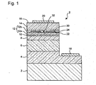
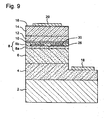
- Fig. 1 is a sectional view showing a gallium nitride semiconductor laser device according to this embodiment.
- An n-side contact layer 4 made of GaN, an n-side cladding layer 6 made of AlGaN, an n-side optical guide layer 8 made of GaN, a multiple quantum well active layer 10 having a well layer containing In, a p-side optical guide layer 12 made of GaN, a p-side cladding layer 14 made of AlGaN and a p-side contact layer 16 made of GaN are formed on a substrate 2 made of a different material such as sapphire.
- Formed in the p-side optical guide layer 12 is a current blocking layer 30 that has a stripe-shaped window 32.
- the current blocking layer 30 is made of a gallium nitride semiconductor that contains Al in ratio of 0.5 or higher and has high resistivity, so as to concentrate the current within the active layer 10 located in the window 32 and control horizontal transverse mode of laser oscillation.
- Fig. 2A and 2B are partially enlarged sectional views showing the structure in the vicinity of the current blocking layer 30 in more detail.
- a carrier confinement layer 11 made of gallium nitride semiconductor containing Al is formed with a thickness from 5 nm to 15 nm (50 to 150 ⁇ ) on the active layer 10 made of gallium nitride semiconductor containing In, and the p-side optical guide layer 12 made of GaN is formed thereon.
- the p-side optical guide layer 12 comprises a first p-side optical guide layer 12a located below the current blocking layer 30 and a second p-side optical guide layer 12b.
- the current blocking layer is formed on the first p-side optical guide layer 12a via a first semiconductor layer 22 and a second semiconductor layer 24, and the window 32 is formed to penetrate the current blocking layer 30 and the second semiconductor layer 24.
- the second p-side optical guide layer 12b is formed so as to fill in the window 32.
- the current blocking layer 30 is not only high in resistance but also low in crystallinity because of the high Al ratio of 0.5 or higher.
- dislocations 40 occur with a high density also in the p-side cladding layer 14 and the p-side contact layer 16 formed above the current blocking layer 30, thus making it difficult for current to flow therein. That is, the current blocking layer 30 exercises current block effect in the semiconductor layer located above it by decreasing the crystallinity thereof, in addition to the current block effect achieved by the resistance of itself. Therefore, even when the current blocking layer 30 is formed with a relatively small thickness of 10 nm to 50 nm (100 to 500 ⁇ ), it can perform sufficient current blocking effect through the combined effect of high resistance and low crystallinity of itself.
- the second semiconductor layer 24 located below the current blocking layer 30 is made of a nitride semiconductor having a mixed crystal ratio of Al lower than that of the current blocking layer 30, so as to function as an etching stopper layer when the window 32 is formed in the current blocking layer 30 by photolithography, and also protect the device layer from ambient gas such as oxygen, before eventually being removed from the current path by etch-back carried in a vapor phase growth apparatus.
- the second semiconductor layer 24 has The Al ratio (preferably 0.1 or less) lower than that of the current blocking layer 30, it is etched with an alkaline solution at a rate different from that of the current blocking layer 30 that has The Al ratio of 0.5 or higher, and therefore remains without being etched when the current blocking layer 30 is etched with an alkaline solution.
- the second semiconductor layer 24 serves as the etching stopper layer and prevents excessive etching.
- the second semiconductor layer 24 is made of a nitride semiconductor having low Al ratio, it reacts at a low rate with oxygen and other elements contained in air.. Therefore, the second semiconductor layer 24 can effectively protect the first semiconductor layer located thereunder from the ambient gas such as oxygen in the photolithography process carried out outside the vapor phase growth apparatus.
- the second semiconductor layer 24 is damaged on the surface thereof through the etching process to remove the current blocking layer 30 and exposure to the atmosphere.
- the second semiconductor layer of this embodiment is made of a nitride semiconductor having lower Al ratio that that of the first semiconductor 22, it easily decomposes when exposed to a reducing gas such as hydrogen at a high temperature.
- the second semiconductor layer 24 that has been damaged can be easily removed from the window 32 that becomes the current path, by the etch-back process carried out in the vapor phase growth apparatus.
- the first semiconductor layer 22 serves as an etching stopper layer during the etch-back process carried out before re-growth on the current blocking layer 30 in the vapor phase growth apparatus and also protects the first p-side optical guide layer 12a located thereunder from gas etching.
- the first semiconductor layer 22 is made of gallium nitride semiconductor having higher Al ratio than the second semiconductor layer and is not easily decomposed when exposed to reducing gas such as hydrogen at a high temperature. Therefore, even when the etch-back process is carried out in the vapor phase growth apparatus for a long period of time so as to completely remove the damaged second semiconductor layer 24, the etch-back process stops at the first semiconductor layer 22 and the first p-side optical guide layer 12a is protected from excessive etching.
- the first semiconductor layer 22 While the first semiconductor layer 22 remains in the current path that leads to the active layer 10, it has better crystallinity and lower resistance than the current blocking layer 30 because it has Al ratio comparable to or lower than that of the current blocking layer and is preferably grown at a higher temperature than that of growing the current blocking layer. Also because it suffices that the first semiconductor layer 22 has the minimum thickness required to function as the etching stopper layer during etch-back, it may be formed in such a thin film that does not block the current injection into the active layer 10, and substantially no increase occurs in the threshold current of laser.
- the gallium nitride semiconductor laser according to this embodiment due to the complementary actions of the first semiconductor layer and the second semiconductor layer, the layer formed through reaction with the atmosphere is prevented from remaining in the window of the current blocking layer 30 and defective shape can be prevented from being formed due to excessive etch-back, thus achieving stable laser characteristics.
- compositions of the p-side cladding layer 14 and the p-side contact layer 16 formed thereon can be restricted from becoming inhomogeneous, so that the functions of the layers are improved.
- the p-side cladding layer 14 has super lattice structure, in particular, it is important that the second p-side optical guide layer 12b fills the window 32 to make a flat surface. Because the super lattice structure is disturbed when there is a step on the surface of the p-side optical guide layer 12 that makes contact with the bottom thereof.
- the region 36 located above the window 32 may be formed thicker than the region 38 located above the current blocking layer 30. That is, since the current blocking layer 30 has low crystallinity, the region 36 located above the window 32 grows faster than the region 38 located above the current blocking layer 30 and therefore the larger the difference in the rate of growth, the thicker becomes the region 36 located above the window 32. It is advantageous for confining light within the waveguide to make the region 36 located above the window 32 thicker. Thickness distribution can be controlled as shown in Fig. 2A or 2B by regulating the crystallinity of the current blocking layer 30. Crystallinity of the current blocking layer 30 can be controlled by regulating the Al ratio or the growing temperature of the current blocking layer 30. The higher the Al ratio of the current blocking layer 30 and the lower the growing temperature, the lower becomes the crystallinity of the current blocking layer 30.
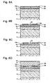
- Fig. 3 is a sectional view showing the structure of the first p-side optical guide layer 12a that has been etched back excessively.
- the first p-side optical guide layer 12a is made of GaN and is therefore easily decomposed when exposed to reducing gas such as hydrogen at a high temperature. As a consequence, once the etch-back proceeds excessively, the etch-back can easily proceed up to the carrier confinement layer 11 that is made of nitride semiconductor containing Al, as shown in Fig. 3.
- the total thickness of the p-side optical guide layer 12 is usually from 150 nm to 200 nm (1500 to 2000 ⁇ ), excessive etch-back of 75 nm to 100 nm (750 to 1000 ⁇ ) can occur.
- core of the waveguide in the region 36 that makes the current path becomes thinner compared to the surrounding region 38, and the efficiency of light confinement decreases.
- inhomogeneous composition tends to occur such as precipitation of Al into the step.
- the p-type cladding layer 14 has super lattice structure, normal super lattice structure may not be maintained due to the influence of the step.
- the first semiconductor layer 22 is made of gallium nitride semiconductor having The Al ratio that is comparable to or lower than that of the current blocking layer 30 and is higher than that of the second semiconductor layer 24.
- the second first semiconductor layer and the current blocking layer are represented as In x1 Al y1 Ga 1-x1-y1 N, In x2 Al y2 Ga 1-x2-y2 N and In x3 Al y3 Ga 1-x3-y3 N, it is preferable that the ratios are such that relation y 2 ⁇ y 1 ⁇ y 3 is satisfied. Durability of the first semiconductor layer 22 against the reducing gas becomes higher as the Al ratio becomes higher.
- the Al ratio y 1 of the first semiconductor layer is preferably 0.1 or higher, and more preferably 0.2 or higher.
- resistance of the first semiconductor layer tends to become higher. Since the first semiconductor layer 22 becomes a part of the current path to the active layer, higher resistance of the first semiconductor layer 22 increases the threshold current of laser oscillation and is not desirable.
- the Al ratio y 1 of the first semiconductor layer is preferably 0.8 or lower, more preferably 0.5 or lower.
- the ratio of In contained in the first semiconductor layer 22 is preferably low. This is because the first semiconductor layer absorbs light emitted from the active layer when it contains In, since the first semiconductor layer 22 is located in the waveguide.
- the first semiconductor layer has an In ratio x1 of 0.1 or lower, and preferably 0.05 or lower, and more preferably the first semiconductor layer essentially does not contain In. From the discussion described above, preferable composition of the first semiconductor layer is Al a Ga 1-a N (0.1 ⁇ a ⁇ 1).
- the thickness of the first semiconductor layer is preferably from 2 nm to 30 nm (20 to 300 ⁇ ), and more preferably from 5 nm to 20 nm (50 to 200 ⁇ ).
- the first semiconductor layer is made of AIN, it can function as the etching stopper layer when the thickness is about 1 nm (10 ⁇ ) or more.
- the layer that makes contact with the bottom of the first semiconductor layer is preferably an optical guide layer. It becomes easier to control the confinement of light when the current blocking structure is formed so as to make contact with the optical guide layer.
- Function of the first semiconductor layer may also be carried out by a cap layer to be described later.
- the cap layer is caused to perform the etching stopper function, layers having high Al ratio can be decreased and therefore the operating voltage can be decreased.
- the second semiconductor layer 24 preferably is made of a gallium nitride semiconductor having lower Al ratio than those of the current blocking layer 30 and the first semiconductor layer 22, namely a gallium nitride semiconductor having a composition represented by the general formula In x2 Al y2 Ga 1-x2-y2 N (0 ⁇ x 2 ⁇ 1, 0 ⁇ y 2 ⁇ y 1 , 0 ⁇ x 2 + y 2 ⁇ 1).
- the lower the Al ratio in the second semiconductor layer the greater the difference in the etching rate between the second semiconductor layer and the current blocking layer 30, thus making it easier to remove by etch-back.
- the second semiconductor layer 24 has the Al ratio y 2 of 0.1 or lower, and preferably 0.05 or lower, and more preferably essentially does not contain Al.
- the second semiconductor layer preferably contains In.
- InN having lower decomposition temperature is contained in the mixed crystal, the layer becomes easier to decompose at a high temperature and can be removed by etch-back more easily.
- In contained in the second semiconductor layer also has an effect of absorbing stray light that has leaked from the active layer.
- light emitted by the active layer that is made of a nitride semiconductor containing In is likely to be absorbed by another nitride semiconductor containing In. Therefore, by making such a constitution as the second semiconductor layer that sandwiches the active region on both sides contain In, stray light that has leaked from the active region can be absorbed and quality of the beam can be improved.
- In ratio x 2 of the second semiconductor layer is preferably in a range from 0 to 0.2, and more preferably from 0.05 to 0.15.
- preferable composition of the second semiconductor layer is In b Ga 1-b N (0.05 ⁇ b ⁇ 0.15).
- the second semiconductor layer is preferably grown with low crystallinity in order to make it easy to remove by etch-back.
- the second semiconductor layer is formed in polycrystalline or amorphous structure. Since the second semiconductor layer of such a structure has a high resistance, combined effect thereof and the current blocking layer formed thereon makes it possible to achieve better current blocking effect. Also because the second semiconductor layer performs part of the current blocking effect, the current blocking layer may be formed with a smaller thickness. Crystallinity of the second semiconductor layer 24 can be made lower by increasing the In ratio x 2 of the second semiconductor layer or decreasing the growing temperature. When the growing temperature of the second semiconductor layer 24 is decreased, it is preferable to set the growing temperature lower than 1000°C, more preferably to 600°C or lower.
- crystallinity of the second semiconductor layer becomes lower, it has an effect of making it easier to remove the current blocking layer 30 that is grown thereon. That is, if the layer that contacts the bottom of the current blocking layer 30 has good crystallinity, crystallinity of the current blocking layer 30 becomes partially higher in the vicinity of the layer boundary, thus making it difficult to remove the portion by etching.
- crystallinity of the second semiconductor layer 24 that makes contact with the bottom of the current blocking layer 30 lower, it is made possible to grow the current blocking layer 30 with low crystallinity from the start of growth, thereby making it easier to remove the current blocking layer 30 in the window 32.
- the second semiconductor layer 24 contains impurity in a concentration of 5 ⁇ 10 17 /cm 3 or higher, more preferably 5 ⁇ 10 18 /cm 3 or higher, crystallinity of the second semiconductor layer 24 becomes lower, thereby making it easier to remove the current blocking layer 30. Also as the second semiconductor layer 24 contains impurities in high concentration, it becomes easier to absorb stray light coming from the active layer, so that oscillation of higher mode can be suppressed and laser beam of stable single mode can be obtained.
- the step formed by the current blocking layer and the second semiconductor layer becomes larger, it becomes difficult to form the cladding layer and the contact layer located above the step in super lattice (SL) structure, resulting in lower carrier mobility and higher operating voltage.
- SL super lattice
- band gap increases which also contributes to the higher operating voltage. Since higher operating voltage leads to larger electric power supplied, it results in larger heat generation and higher threshold.
- the thickness of the second semiconductor layer is preferably from 1 nm to 30 nm (10 to 300 ⁇ ), and more preferably from 5 nm to 20 nm (50 to 200 ⁇ ).
- the current blocking layer 30 is made of a nitride semiconductor having a composition represented by the general formula In x3 Al y3 Ga 1-x3-y3 N (0 ⁇ x 3 ⁇ 0.1, 0.5 ⁇ y 3 ⁇ 1, 0.5 ⁇ x 3 + y 3 ⁇ 1).
- Forming the current blocking layer 30 from the gallium nitride semiconductor represented by the above general formula instead of an insulating material such as SiO 2 , makes it possible to grow the current blocking layer 30 in the same vapor phase growth apparatus as that for the other device structure.
- Forming the current blocking layer 30 from the gallium nitride semiconductor instead of a different material such as SiO 2 also has an effect of improving the linearity of the laser beam.
- SiO 2 is embedded in an optical guide layer or the like made of GaN, for example, significant difference between the refractive index of SiO 2 , about 1.5, and the refractive index of GaN, that is 2.5, causes a deviation of the laser output from linearity and the beam to fluctuate. Although the beam may be stabilized by making the current path narrower, it results in higher current density and shorter service life. If AlN is used for the current blocking layer, in contrast, there is a smaller difference in refractive index which is 2.1 for AIN and 2.5 for GaN, thus the linearity is improved and the beam is stabilized.
- the Al ratio y 3 in the current blocking layer 30 is at least 0.5 or higher, preferably 0.75 or higher, and more preferably 0.9 or higher.
- the current blocking layer 30 is made of AIN.
- the current blocking layer 30 may contain a small amount of In. Making the current blocking layer 30 containing a small amount of In makes it easier to absorb light emitted by the active layer 10. Putting the current blocking layer 30 having such a constitution on the active region makes it possible to absorb stray light leaking from the active region and improve the beam property.
- In the ratio x 3 is set to 0.01 or higher, preferably 0.05 or higher, and more preferably 0.1 or higher. However, it is preferable to control the In ratio to 0.5 or lower, preferably 0.3 or lower, more preferably 0.2 or lower and most preferably 0.15 or lower.
- the current blocking layer 30 is preferably grown at a low temperature, 600°C or lower, for example, so that it is grown with low crystallinity. Growing the current blocking layer 30 at a low temperature makes it easier to process it by etching with an alkaline solution or the like and improves the current blocking effect. When the current blocking layer 30 is too thin, it cannot perform the current blocking function sufficiently, while the light confinement effect becomes weaker and the threshold increases. When the current blocking layer 30 is too thick, on the other hand, the influence of the step becomes greater, it becomes difficult to form a flat surface when re-growing and it also becomes difficult to form the cladding layer in super lattice (SL) structure. Thus the thickness of the current blocking layer 30 is preferably from 10 nm to 50 nm (100 to 500 ⁇ ), and more preferably from 15 nm to 30 nm (150 to 300 ⁇ ).
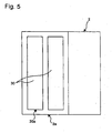
- the current blocking layer 30 it is also preferable to form the current blocking layer 30 so that the end face thereof in the longitudinal direction 30a is located inward from the end face 2a of the resonator of the laser device 2, as shown in Fig. 5.
- energy density at the end face 2a of the resonator becomes lower and COD (catastrophic optical damage) characteristic can be improved. It provides also such a benefit that defective shape and cracks become less likely to occur in the waveguide when forming the end face of resonator by RIE or cleavage.
- the resonator surface is formed by etching, it becomes easier to form a flat resonator surface when the current blocking layer 30 is formed apart from the end face of the resonator. This is because, since there is the step in the window of the current blocking layer 30, it becomes difficult to form flat etching surface due to the influence of the step when the current blocking layer 30 reaches the end face of the resonator.
- Side face of the current blocking layer 30 in the lateral direction is also preferably formed inward of the side face of the laminate that constitutes the stripe structure of the laser device 2 as shown in Fig. 5.
- the current blocking layer having high a mixed crystal ratio of Al is difficult to etch uniformly, and is likely to have rough surface formed by etching.
- etching the laminate of the nitride semiconductor layers to form an n electrode may cause rough etching surface and higher connection resistance of the n electrode. If the current blocking layer 30 is formed within a region inward from the side face of the stripe structure, it becomes easier to carry out etching to form the n electrode and the resistance thereof can be decreased.
- the current blocking layer has a high a mixed crystal ratio of Al and therefore has lattices constant and thermal expansion coefficient that are significantly different from those of the layers located above and below thereof.
- the current blocking layer 30 is formed within a region located apart from the end face and/or the side face of the laminate that constitutes the stripe structure to such an extent that does not affect the current blocking effect and the light confinement function, namely within the inner region, strain can be reduced and cracks can be suppressed from occurring.
- the semiconductor layers that are re-grown while filling the window 32 of the current blocking layer 30 are made of a nitride semiconductor which essentially does not contain Al, preferably GaN, it becomes easier to fill in the widow 32 into a flat surface and the problem of uneven distribution of Al in the re-growth layer formed in the window can be solved. Uneven distribution of Al has greater influence on the laser device characteristic than the uneven concentration of impurities such as Mg.
- the layer re-grown by filling the window 32 is preferably an optical guide layer rather than a cladding layer. By forming the re-growth layer as the optical guide layer, it becomes easier to fill in the window and grow flat, and it is made possible to improve the characteristics of the cladding layer of super lattice structure.
- the re-growth layer preferably has a refractive index comparable to or lower than that of the layer that makes contact with the bottom of the first semiconductor layer 22. This further improves the effect of confining light in the active layer. It is also preferable to grow the re-growth layer at such a temperature that is comparable to or higher than that of the layer that makes contact with the bottom of the first semiconductor layer 22 and is suitable for maintaining the crystallinity of the active layer. Higher growing temperature improves the crystallinity of the re-growth layer and decreases the resistance.
- the re-growth layer preferably contains impurities in a concentration that is comparable to or higher than that of the layer that makes contact with the bottom of the first semiconductor layer 22.
- Higher impurity concentration in the re-growth layer stabilizes the higher mode of laser oscillation as the stray light is absorbed in portions on both sides of the window.
- the re-growth layer may also be advantageously turned into p-type so as to decrease the operating voltage, by intentionally adding a p-type impurity such as Mg to the re-growth layer.
- the active layer 10 is preferably made of gallium nitride semiconductor where at least the light emitting region contains In, and more preferably has such a multiple quantum well structure (MQW structure) as In x1 Ga 1-x1 N well layers (0 ⁇ X 1 ⁇ 1) and In x2 Ga 1-x2 N barrier layers (0 ⁇ X 2 ⁇ 1, X 1 >X 2 ) are stacked alternately a required number of times.
- MQW structure multiple quantum well structure
- the well layer is preferably formed undoped, while all barrier layers are doped with n-type impurity such as Si or Sn in concentration from 1 ⁇ 10 17 to 1 ⁇ 10 19 /cm 3 .
- the active layer 10 may end with a well layer or end with a barrier layer. Since the active layer 10 contains a relatively high content of InN that has a high vapor pressure to form a mixed crystal, it is easy to decompose and can be grown at a lower temperature (not higher than about 900°C) than the other layers.
- the carrier confinement layer 11 is made of p-type gallium nitride semiconductor having a higher mixed crystal ratio of Al than the p-side cladding layer 14, and preferably has a composition of Al c Ga 1-c N (0.1 ⁇ c ⁇ 0.5). Thickness of the carrier confinement layer 11 is preferably from 5 nm to 20 nm (50 to 200 ⁇ ).
- the carrier confinement layer 11 is doped with p-type impurity such as Mg in a high concentration, preferably from 5 ⁇ 10 17 to 1 ⁇ 10 19 /cm 3 . With such a constitution, the carrier confinement layer 11 can effectively confine electrons within the active layer and decreases the threshold of the laser.
- the carrier confinement layer 11 also has the function to protect the active layer 10 that contains In and therefore easily decomposes. That is, since the carrier confinement layer 11 is made of AlGaN that has high decomposition temperature, it can effectively protect the active layer 10 from decomposition.
- the carrier confinement layer 11 is preferably grown at a low temperature not higher than 900°C in an inert gas such as nitrogen so that the active layer 10 will not be decomposed.
- the n-side optical guide layer 8 and the p-side optical guide layer 12 are preferably made of gallium nitride semiconductor that essentially does not contain Al.
- these layers are made of In d Ga 1-d N (0.1 ⁇ d ⁇ 1) , and more preferably made of GaN.
- the p-side optical guide layer is divided into two layers of first p-side optical guide layer 12a and second p-side optical guide layer 12b, and the current blocking layer 30 is formed between these layers.
- the second p-side optical guide layer 12b in such a composition that does not essentially contain Al, it becomes easier to achieve a flat surface when the current blocking layer 30 is embedded.
- the first p-side optical guide layer 12a and the second p-side optical guide layer 12b may have different compositions and may be formed in different processes.
- the second p-side optical guide layer 12b in particular, preferably has lower refractive index and higher impurity concentration and is grown at a higher temperature than the first p-side optical guide layer. The same applies also to a case of embedding the current blocking layer 30 in the n-side optical guide layer.
- the n-side cladding layer 6 and the p-side cladding layer 14 are preferably formed by stacking nitride semiconductor layers, that have different levels of band gap energy of which at least one includes nitride semiconductor layer that contains Al, in super lattice structure.
- nitride semiconductor layer that contains Al Al e Ga i-e N (0 ⁇ e ⁇ 1) is preferably used.
- super lattice structure is formed by stacking GaN and AlGaN. Since the mixed crystal ratio of Al of the entire cladding layer can be increased by forming the n-side cladding layer 6 and the p-side cladding layer 14 in super lattice structure, threshold of the laser can be decreased.
- number of pits formed in the cladding layer can be decreased by forming it in super lattice structure.
- Crystallinity can also be improved by modified doping, wherein one of the layers that constitute the super lattice structure is doped more heavily than another. Doping may also be applied similarly to both layers.
- a p-side ohmic electrode 20 is formed on the p-side contact layer 16.
- the material to form the p-side electrode 20 Ni, Co, Fe, Cr, Al, Cu, Au, W, Mo, Ta, Ag, Pt, Pd, Rh, Ir, Ru, Os and oxides and nitrides of these elements may be used, in the form of single layer, alloy or multi-layer film.
- at least one kind selected from among Ni, Co, Fe, Cu, Au and Al, or oxide or nitride of these elements may be used.
- Such a 2-layer structure is preferable that comprises an ohmic electrode provided in contact with the semiconductor layer and a pad electrode provided thereon.
- Ni/Au/Pt Ni/Au/Rh oxide, Pd/Pt, Ni/Au, Co/Au or the like. It is also preferable that such a structure as described above is formed as the ohmic electrode that makes contact with the semiconductor layer, and the pad electrode is formed separately thereon.
- the pad electrode may also be made of a material similar to those described above, and it is preferable to use a metal of platinum group or oxide thereof in the interface with the ohmic electrode which improves thermal stability.
- Width of the p-side ohmic electrode 20 is preferably larger than the width of the window 32 and smaller than the width of the current blocking layer 30 (total width including window). By forming the p-side ohmic electrode 20 with such a width, it is made possible to efficiently inject current into the window. Length of the p-side ohmic electrode 20 in the direction substantially parallel to the laser beam guiding direction is preferably shorter than the length of the current blocking layer 30. By forming the p-side ohmic electrode 20 with such a length, it is made possible to more efficiently inject current into the window.
- Ni, Co, Fe, Ti, Cu, Au, W, Zr, Mo, Ta, Al, Ag, Pt, Pd, Rh, Ir, Ru, Os or the like may be used, in the form of single layer, alloy or multi-layer film.
- Ti/Al, V/Al, V/Pt/Au, Ti/Mo/Ti/Pt/Au or Ti/W/Ti/Pt/Au may be used.
- Ti/Mo/Ti/Pt/Au and Ti/W/Ti/Pt/Au are especially preferable in case heavy load is applied to the electrode during high output operation since they are laminates wherein a layer made of a material having high melting point such as Pt is interposed, thus such constitutions are thermally stable.
- FIG. 4 is a process diagram showing the method of manufacturing the gallium nitride semiconductor laser according to this embodiment.
- the first semiconductor layer 22 made of In x1 Al y1 Gal 1-x1-y1 N (0 ⁇ x 1 ⁇ 0.1, y 2 ⁇ y 1 ⁇ y 3 , 0 ⁇ x 1 + y 1 ⁇ 1)
- the second semiconductor layer 24 made of In x2 Al y2 Ga 1-x2-y2 N (0 ⁇ x 2 ⁇ 1, 0 ⁇ y 2 ⁇ y 1 , 0
- the first semiconductor layer is preferably grown at a high temperature comparable to that for growing the n-side or p-side cladding layer of the laser, for example 1000°C or higher.
- a high temperature comparable to that for growing the n-side or p-side cladding layer of the laser, for example 1000°C or higher.
- the second semiconductor layer 24 and the current blocking layer 30, are preferably grown at a low temperature below 1000°C, preferably 600°C or lower.
- the wafer is taken out of the reaction vessel of the vapor phase growth apparatus and the window 32 is formed in the current blocking layer 30 by photolithography using a photo resist 34.
- Etching of the current blocking layer 30 is preferably carried out by wet etching that is less likely to cause damage to the device, rather than dry etching.
- the gallium nitride semiconductor having high Al ratio such as AIN, for example, easily dissolves in an alkaline developer solution such as tetramethylammonium hydroxide (TMAH), and therefore can be processed to pattern the current blocking layer 30 by photolithography using an alkaline solution as the developer.
- TMAH tetramethylammonium hydroxide
- the second semiconductor layer 24 on the other hand, has low Al ratio and therefore does not dissolve in an alkaline solution, and functions as an etching stopper layer. At the same time, the second semiconductor layer 24 also protects a portion of the semiconductor layer located in the waveguide from the alkaline solution and the oxygen contained in the atmosphere.
- the wafer is put into the reaction furnace of the vapor phase growth apparatus again, and is kept at a high temperature of 1000°C or higher while flowing a reducing gas such as hydrogen, so as to carry out etch-back.
- a reducing gas such as hydrogen
- the first semiconductor layer 22 is made of gallium nitride semiconductor having high Al ratio and therefore does not easily decompose even in a reducing gas such as hydrogen at a high temperature, and functions as the etching stopper layer against etch-back.
- the second p-side optical guide layer 12b is grown on the current blocking layer 30 so as to fill the window 32 and make a flat surface.
- the window 32 can be easily filled to be flat when the second p-side optical guide layer 12b is made of a nitride semiconductor that essentially does not contain Al, preferably GaN.
- the second p-side optical guide layer 12b that is the semiconductor used to fill the window 32 of the current blocking layer 30 preferably has refractive index comparable to or lower than that of the first p-side optical guide layer 12a that makes contact with the bottom of the first semiconductor layer. With this constitution, more effective confinement of light can be achieved.
- the second p-side optical guide layer 12b that is the semiconductor used to fill the window 32 of the current blocking layer 30 is preferably grown at such a temperature that is comparable to or higher than that of growing the first p-side optical guide layer 12a that is the layer which makes contact with the bottom of the first semiconductor layer and is suitable for maintaining the crystallinity of the active layer. Higher growing temperature improves the crystallinity of the semiconductor layer which is re-grown while filling in the window, and decreases the resistance.
- the p-side cladding layer 14 and the p-side contact layer 16 may be grown successively by the ordinary method of manufacturing the gallium nitride semiconductor laser.
- the current blocking layer 30 is formed in the p-side optical guide layer 12 in the first embodiment, the current blocking layer 30 is formed in the n-side optical guide layer 8 in this embodiment. With other respects, this embodiment is similar to the first embodiment.
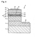
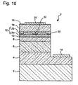
- Fig. 6 is a sectional view showing a gallium nitride semiconductor laser according to the second embodiment.
- the current blocking layer 30 having the window 32 of stripe configuration is formed in the n-side optical guide layer 8.
- the current blocking layer 30 is made of In x3 Al y3 Ga 1-x3-y3 N (0 ⁇ x 3 ⁇ 0.1, 0.5 ⁇ y 3 ⁇ 1, 0.5 ⁇ x 3 + y 3 ⁇ 1) having high resistivity, and plays the role of controlling the horizontal transverse mode of the laser oscillation by concentrating current in the window 32.
- the n-side optical guide layer 8 comprises a first n-side optical guide layer 8a that is located below the current blocking layer 30 and a second n-side optical guide layer 8b.
- the current blocking layer 30 is formed above the first n-side optical guide layer 8a via the first semiconductor layer 22 and the second semiconductor layer 24, while the window 32 is formed to penetrate the current blocking layer 30 and the second semiconductor layer 24.
- the second n-side optical guide layer 8b is formed so as to fill the window 32.
- the second semiconductor layer 24 is made of gallium nitride semiconductor having lower Al ratio than those of the current blocking layer 30 and the first semiconductor layer, so as to function as an etching stopper layer when the window 32 is formed in the current blocking layer 30 by photolithography and protects the first semiconductor layer 22 from the ambient gas such as oxygen, to be eventually removed in the etch-back process carried out in the vapor phase growth apparatus.
- the first semiconductor layer 22 functions as the etching stopper layer during the etch-back process carried out before re-growing onto the current blocking layer 30 in the vapor phase growth apparatus, and protects the first n-side optical guide layer 8a located below thereof from gas etching.
- the layer formed through reaction with the atmosphere is prevented from remaining in the window of the current blocking layer 30 and defective shape can be prevented from being formed due to excessive etch-back, so that stable laser characteristic can be obtained.
- the second semiconductor layer having lower Al ratio is formed below the current blocking layer, and the first semiconductor layer having higher Al ratio is formed further below thereof, so as to prevent excessive etch-back from occurring by means of the first semiconductor layer.
- only a growth base layer having low Al ratio is provided below the current blocking layer, and crystallinity of the growth base layer is controlled to be lower than that of the layer that makes contact with the bottom of the growth base layer, so as to prevent excessive etch-back.
- this embodiment is similar to the first embodiment.
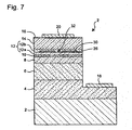
- Fig. 7 is a sectional view showing the gallium nitride semiconductor laser according to the third embodiment, the n-side contact layer 4 made of GaN, the n-side cladding layer 6 made of AlGaN, the n-side optical guide layer 8 made of GaN, the multiple quantum well active layer 10 having a well layer containing In, the p-type optical guide layer 12 made of GaN, the p-side cladding layer 14 made of AlGaN and the p-side contact layer 16 made of GaN are formed on the substrate 2 made of sapphire or the like. Formed in the p-type optical guide layer 12 is the current blocking layer 30 that has the stripe-shaped window 32.
- the current blocking layer 30 is made of In x Al y Ga 1-x-y N (0 ⁇ x ⁇ 0.1, 0.5 ⁇ y ⁇ 1, 0.5 ⁇ x + y 1) that has high resistivity, so as to concentrate the current in the active layer 10 within the window 32 and control horizontal transverse mode of laser oscillation.
- the p-side optical guide layer 12 comprises the first p-side optical guide layer 12a located below the current blocking layer 30 and the second p-side optical guide layer 12b.
- the current blocking layer 30 is formed on the first p-side optical guide layer 12a via the growth base layer 26, and the window 32 is formed to penetrate the current blocking layer 30 and the growth base layer 26.
- the second p-side optical guide layer 12b is formed so as to fill in the window 32.
- the growth base layer 26 is made of a nitride gallium semiconductor having Al ratio lower than that of the current blocking layer 30, so as to function as an etching stopper layer when the window 32 is formed in the current blocking layer 30 by photolithography and also protect the p-type optical guide layer 12a located below thereof from ambient gas such as oxygen, before eventually being removed by etch-back carried in a vapor phase growth apparatus.
- the growth base layer 26 has low Al ratio (preferably 0.05 or less), and it is etched with an alkaline solution at a rate different from that of the current blocking layer 30 that has Al ratio of 0.5 or higher, and therefore remains without being etched when the current blocking layer 30 is etched with alkaline solution.
- the growth base layer 26 serves as the etching stopper layer and prevents excessive etching.
- the growth base layer 26 is made of the nitride gallium semiconductor having low Al ratio, it reacts with oxygen and other elements contained in air only at a slow rate. Therefore, the growth base layer 26 can effectively protect the first p-side optical guide layer 12a located thereunder from the ambient gas such as oxygen in the photolithography process carried out outside the vapor phase growth apparatus.
- the growth base layer 26 is damaged on the surface thereof through the etching process by the photolithography and through exposure to the atmosphere.
- the growth base layer 26 is made of a nitride semiconductor that essentially does not contain Al, it easily decomposes when exposed to a reducing gas such as hydrogen at a high temperature. As a result, the growth base layer 26 that has been damaged can be easily removed from the window 32 that becomes the current path, by etching back in the vapor phase growth apparatus.
- the growth base layer 26 is made with lower crystallinity than the first p-side optical guide layer that makes contact with the bottom thereof, thereby generating a difference in the etching rate for etch-back between these layers. That is, by making the growth base layer 26 with lower crystallinity than the first p-side optical guide layer, etch-back is caused to proceed fast in the growth base layer 26 and slowly in the first p-side optical guide layer 12a. This makes it possible to selectively remove the growth base layer 26 only.
- the layer formed through reaction with the atmosphere is prevented from remaining in the window of the current blocking layer 30 and defective shape can be prevented from being formed due to excessive etch-back, so that stable laser characteristic can be obtained.
- the growth base layer 26 is made of gallium nitride semiconductor having lower Al ratio that the current blocking layer 30, namely a gallium nitride semiconductor having a composition represented by the general formula In x' Al y' Ga 1-x' - y' N (0 ⁇ x' ⁇ 1, 0 ⁇ y' ⁇ y, 0 ⁇ x' + y' ⁇ 1).
- the growth base layer 26 preferably contains In.
- In ratio x' in the growth base layer 26 is preferably from 0 to 0.2, and more preferably 0.05 to 0.15.
- preferable composition of the growth base layer 26 is In f Ga 1-f N (0 ⁇ f ⁇ 0.2).
- In ratio in the growth base layer may be made higher than that of the layer that makes contact therewith from below, or the growth base layer may be grown at a lower temperature than the layer that makes contact therewith from below.
- the growth base layer 26 can be selectively removed when the In ratio of the growth base layer 26 is higher than that of the first p-side optical guide layer 12a.
- Capability of the growth base layer 26 to absorb stray light from the active layer can be increased by forming the growth base layer 26 with higher impurity concentration (for example, 5 ⁇ 10 18 /cm 3 or higher) or containing In. This makes it possible to suppress the oscillation in higher mode and generate stable laser beam of single mode.
- the growing temperature is preferably set to 900°C or lower, and more preferably 600°C or lower.
- the means for lowering the crystallinity of the growth base layer 26 both means of increasing the In ratio and lowering the growing temperature may be used in combination.
- the growth base layer 26 is preferably made in amorphous or polycrystalline structure. By making the growth base layer 26 in amorphous or polycrystalline structure, it becomes easier to remove than single crystal. Also because resistivity of the growth base layer becomes higher, better current blocking effect can be achieved through combined effect of the high resistivity and the current blocking layer formed in contact thereon. It is also made possible to make the current blocking layer thinner.
- Forming the growth base layer 26 with low crystallinity also has such an effect that it becomes easier to remove the current blocking layer 30 that is grown thereon.
- the layer that makes contact with the bottom of the current blocking layer 30 is good, a part of the current blocking layer 30 near the interface has good crystallinity and becomes difficult to remove by etching. Accordingly, the current blocking layer 30 has low crystallinity from the early stage of growth and it becomes easier to remove the current blocking layer 30 from within the window 32, bye forming the growth base layer 26 that makes contact with the bottom of the current blocking layer 30 with low crystallinity.
- the growth base layer 26 cannot protect the first p-type optical guide layer 12a sufficiently when it is too thin, and allows the step to cause greater influence when it is too thick. When the step is larger, it becomes difficult to form the semiconductor layer to be re-grown on the current blocking layer with flat surface. Therefore, the thickness of the growth base layer 26 is preferably from 1 nm to 30 nm (10 to 300 ⁇ ), and more preferably from 5 nm to 20 nm (50 to 200 ⁇ ).
- the layer that makes contact with the bottom of the growth base layer 26 is preferably an optical guide layer. It becomes easier to control the confinement of light by forming the current blocking structure so as to make contact with the optical guide layer.
- FIG. 8 is a process diagram showing the method of manufacturing the gallium nitride semiconductor laser according to the third embodiment.
- the growth base layer 26 made of In x Al y Ga 1-x'-y' N (0 ⁇ x' ⁇ 1, 0 ⁇ y' ⁇ y, 0 ⁇ x' + y' ⁇ 1) and the current blocking layer 30 made of In x Al y Ga 1-x-y N (0 ⁇ x ⁇ 0.1, 0.5 ⁇ y ⁇ 1, 0.5 ⁇ x + y ⁇ 1) are grown successively.
- the growth base layer 26 made of In x Al y Ga 1-x'-y' N (0 ⁇ x' ⁇ 1, 0 ⁇ y' ⁇ y, 0 ⁇ x' + y' ⁇ 1)
- the current blocking layer 30 made of In x Al y Ga 1-x-y N (0 ⁇ x ⁇ 0.1, 0.5 ⁇ y ⁇ 1, 0.5 ⁇ x + y ⁇ 1)
- the wafer is taken out of the reaction furnace of the vapor phase growth apparatus and the window 32 is formed in the current blocking layer 30 by photolithography using the photo resist 34.
- Patterning of the current blocking layer 30 is preferably carried out by photolithography using an alkaline developer solution such as tetramethylammonium hydroxide (TMAH).
- TMAH tetramethylammonium hydroxide
- the growth base layer 26 has low Al ratio and is therefore difficult to dissolve in tetramethylammonium hydroxide (TMAH), so as to function as an etching stopper layer.
- the growth base layer 26 also protects the portion of the semiconductor layer located in the waveguide from oxygen contained in the atmosphere.
- the wafer is put into the reaction furnace of the vapor phase growth apparatus again and is kept at a high temperature of 1000°C or higher while flowing a reducing gas such as hydrogen, so as to carry out etch-back.
- a reducing gas such as hydrogen
- the growth base layer 26 has been damaged by oxygen or other element contained in the atmosphere during the process shown in Fig. 8B, it is formed so as to have lower crystallinity than the first p-side optical guide layer 12a and therefore the portion thereof exposed through the window 32 is selectively removed by etch-back.
- the first p-side optical guide layer 12a functions as the etching stopper layer against etch-back.
- the second p-side optical guide layer 12b is grown on the current blocking layer 30 so as to fill the window 32 to make a flat surface.
- the window 32 can be easily filled to be flat when the second p-side optical guide layer 12b is made of a nitride semiconductor that essentially does not contain Al, preferably GaN.
- the second p-side optical guide layer 12b that is the semiconductor used to fill the window of the current blocking layer 30 preferably has refractive index comparable to or lower than that of the first p-side optical guide layer 12a that makes contact with the bottom of the growth base layer. With this constitution, more effective confinement of light can be achieved.
- the second p-side optical guide layer 12b that is the semiconductor used to fill the window of the current blocking layer 30 is preferably grown at such a temperature that is comparable to or higher than that of the layer that makes contact with the bottom of the growth base layer and is suitable for maintaining the crystallinity of the active layer. Higher growing temperature improves the crystallinity of the semiconductor layer which is re-grown while filling in the window, and decreases the resistance.
- the p-side cladding layer 14 and the p-side contact layer 16 may be grown successively by the ordinary method of manufacturing the gallium nitride semiconductor laser.
- the current blocking layer 30 is formed in the p-side optical guide layer 12 in the third embodiment, the current blocking layer 30 is formed in the n-side optical guide layer 8 in this embodiment. With other respects, this embodiment is similar to the third embodiment.
- Fig. 9 is a sectional view showing a gallium nitride semiconductor laser according to the fourth embodiment.
- the current blocking layer 30 having the window 32 of stripe configuration is formed in the n-side optical guide layer 8.
- the current blocking layer 30 is made of In x Al y Ga 1-x-y N (0 ⁇ x ⁇ 0.1, 0.5 ⁇ y ⁇ 1, 0.5 ⁇ x + y ⁇ 1) having high resistivity, and plays the role of controlling the horizontal transverse mode of the laser oscillation by concentrating current in the window 32.
- the n-side optical guide layer 8 comprises the first n-side optical guide layer 8a that is located below the current blocking layer 30 and the second n-side optical guide layer 8b.
- the current blocking layer 30 is formed above the first n-side optical guide layer 8a via the growth base layer 26, and the window 32 is formed to penetrate the current blocking layer 30 and the growth base layer 26.
- the second n-side optical guide layer 8b is formed so as to fill the window 32.
- the growth base layer 26 is formed from nitride semiconductor that essentially does not contain Al, so as to have lower crystallinity than the first n-side optical guide layer 8a.
- the growth base layer 26 functions as an etching stopper layer when the window 32 is formed in the current blocking layer 30 by photolithography and protects the first n-side optical guide layer 8a from the ambient gas such as oxygen, to be eventually removed selectively in the etch-back process carried out in the vapor phase growth apparatus.
- the layer formed through reaction with the atmosphere is prevented from remaining in the window of the current blocking layer 30 and defective shape can be prevented from being formed due to excessive etch-back, so that stable laser characteristic can be obtained.
- Fig. 10 is a sectional view showing the gallium nitride semiconductor laser according to this embodiment,
- the n-side contact layer 4 made of GaN, the n-side cladding layer 6 made of AlGaN, the n-side optical guide layer 8 made of GaN, the multiple quantum well active layer 10 having a well layer containing In, the p-type optical guide layer 12 made of GaN, the p-side cladding layer 14 made of AlGaN and the p-side contact layer 16 made of GaN are formed on the substrate 2 made of a different material such as sapphire.
- Formed in the p-side optical guide layer 12 is the current blocking layer 30 that has the stripe-shaped window 32.
- the current blocking layer 30 is made of gallium nitride semiconductor that has Al ratio of 0.5 or higher and high resistivity, so as to concentrate the current in the active layer 10 within the window 32 and control horizontal transverse mode of laser oscillation.
- Fig. 11 A and 11B are partially enlarged sectional views showing the structure of a region in the vicinity of the current blocking layer 30 in more detail.
- the carrier confinement layer 11 made of gallium nitride semiconductor containing Al is formed in a thin film of 5 nm to 20 nm (50 to 200 ⁇ ) on the active layer 10 made of gallium nitride semiconductor, and the p-type optical guide layer 2 made of GaN is formed thereon.
- the p-type optical guide layer 12 comprises the first p-type optical guide layer 12a located below the current blocking layer 30 and the second p-type optical guide layer 12b.
- the current blocking layer is formed on the first p-type optical guide layer 12a and the window 32 is formed in the current blocking layer 30.
- the second p-type optical guide layer 12b is formed so as to fill in the window 32.
- the current blocking layer 30 blocks the current in a portion 30a that encloses the window (hereafter called the main portion), and causes the current to flow through the window 32 into the active layer.
- the main portion 30a of the current blocking layer is not only high in resistance but is also extremely low in crystallinity on the surface because of the Al ratio as high as 0.5.
- dislocations 40 occur with a high density also in the p-side cladding layer 14 and in the p-side contact layer 16 formed above the main portion 30a of the current blocking layer, thus making it difficult for current to flow therein.
- the current blocking layer 30 has current blocking effect in the semiconductor layer located above the main portion 30a due to low crystallinity thereof, in addition to the current blocking effect due to the resistance of the main portion 30a. Therefore, even when the current blocking layer 30 is formed with a relatively small thickness of several hundreds of angstrom, it has sufficient current blocking effect through the combined effect of high resistance and low crystallinity.
- the window 32 of the current blocking layer 30 is formed so that a portion of the current blocking layer 30 that contacts the first p-side optical guide layer 12a, which is the base layer, remains with a thickness of 1 nm (10 ⁇ ) or more.
- the portion of the current blocking layer remaining in the window 32 (hereafter referred to simply as the remaining film portion) 30b has good crystallinity due to the influence of good crystallinity of the first p-side optical guide layer 12a, that is the base layer, and has therefore low resistance.
- substantially no dislocations occur above the remaining film portion 30b of the current blocking layer, as shown in Fig. 11A.
- current can be injected efficiently into the active layer within the window 32, despite the presence of the remaining film portion 30b of the current blocking layer that has high Al ratio.
- the remaining film portion 30b of the current blocking layer has high Al ratio and good crystallinity, it decomposes very slowly in the reducing atmosphere such as hydrogen, and functions as the etching stopper layer when the oxide layer or the like is removed from the wafer surface by etch-back prior to re-growth.
- the remaining film portion 30b of the current blocking layer 30 is also decomposed by the etch-back using hydrogen or the like, the rate of decomposition is very slow and therefore even the etch-back process that is carried out for a sufficient period of time to completely remove the oxide layer or the like formed on the surface of the current blocking layer 30 does not penetrate the remaining film portion 30b of the current blocking layer 30 and erode the p-side guide layer 12a located below.
- a mean thickness remaining after etch-back is set to 1 nm (10 ⁇ ) or more, preferably 3 nm (30 ⁇ ) or more.
- a mean thickness remaining after etch-back of the remaining film portion 30b is preferably less than 10 nm (100 ⁇ ), and more preferably less than 7 nm (70 ⁇ ).
- the crystal grows at a faster rate in a region 36 located above the remaining film portion 30b than in the region 38 located above the main portion 30a, since the main portion 30a of the current blocking layer has lower crystallinity and the remaining film portion 30b has good crystallinity.
- the window 32 which is a recess can be easily filled and made flat with the second p-side optical guide layer 12b.
- compositions of the p-side cladding layer 14 and the p-side contact layer 16 formed thereon can be restricted from becoming uneven, so that the functions of the layers are improved.
- the p-side cladding layer 14 has super lattice structure, in particular, the super lattice structure is disturbed when there is a step on the surface of the second p-side optical guide layer 12b that is the base layer, and therefore it is important that the second p-side optical guide layer 12b fills the window 32 to make a flat surface.
- the device layers (the second p-side optical guide layer, the p-side cladding layer and the p-side contact layer) in the region 36 above the remaining film portion 30b may also be formed to be thicker than the region 38 located above the main portion 30a, as shown in Fig. 11B. Since the main portion 30a of the current blocking layer has low crystallinity, crystal grows faster in the region 36 located above the remaining film portion 30b than in the region 38 located above the main portion 30a. As a result, the device layers in the region 36 located above the remaining film portion 30b can be made thicker than the surrounding area if the difference in growing rate becomes greater. Since the device layers in the region 36 located above the remaining film portion 30b constitute the core portion that surrounds the active region of the laser, it is advantageous for confinement of light to make this portion thicker.
- Such a film thickness distribution as shown in Fig. 11A or 11B can be obtained by controlling the crystallinity of the main portion 30a and the remaining film portion 30b of the current blocking layer. Crystallinity of these layers can be controlled by means of such factors as the Al ratio in the current blocking layer 30, growing temperature, total thickness, thickness of the remaining film portion 30b, crystallinity of the base layer. The better the crystallinity of the base layer of the current blocking layer and the thinner the remaining film portion 30b, the higher the crystallinity of the remaining film portion 30b of the current blocking layer becomes.
- the current blocking layer 30 is preferably carried out at a low temperature so that the main portion 30a has low crystallinity in the surface thereof.
- the growing temperature is, for example, preferably 900°C or lower and more preferably 600°C or lower.
- Growing the current blocking layer 30 at a low temperature makes it easier to process it by etching with an alkaline solution or the like and improves the current blocking effect.
- a total thickness of the current blocking layer 30 (that is the thickness of the main portion 30a) is preferably from 10 nm 80 nm (100 to 800 ⁇ ), and more preferably from 15 nm to 50 nm (150 to 500 ⁇ ).
- the current blocking layer 30 is formed on a base layer that has crystallinity higher than at least that of the current blocking layer 30 itself. Crystallinity better than that of the current blocking layer, of which purpose is insulation, can be obtained as long as the layer constitutes an ordinary gallium nitride semiconductor laser and is formed in the current path.
- the current blocking layer 30 except for the residual film so that the end face thereof in the longitudinal direction 30a is located inward from the end face 2a of the resonator of the laser device 2, as shown in Fig. 5.
- the current blocking layer 30 is formed short of the end face 2a of the resonator, energy density at the end face 2a of the resonator becomes lower and COD (catastrophic optical damage) characteristic can be improved.
- COD catastrophic optical damage
- the resonator surface is formed by etching, it becomes easier to form a flat resonator surface when the current blocking layer 30 is formed apart from the end face of the resonator. This is because, since certain level of step is generated in the window of the current blocking layer 30, it becomes difficult to form flat etching surface due to the influence of the step when the current blocking layer 30 reaches the end face of the resonator. As for the remaining film portion of the current blocking layer, there is not problem if it is formed to reach the end face of the resonator 2a, since it is a thin film where current flows
- Side face of the current blocking layer 30 in the lateral direction is also preferably formed inward of the side face of the laminate that constitutes the stripe structure of the laser device 2 as shown in Fig. 5.
- the current blocking layer having high Al ratio is difficult to etch uniformly, and is likely to have rough surface formed by etching.
- etching the laminate of the nitride semiconductor layers to form an n electrode may cause rough etching surface and higher connection resistance of the n electrode. If the current blocking layer 30 is formed within a region inward from the side face of the stripe structure, it becomes easier to carry out etching to form the n electrode and the resistance decreases
- the current blocking layer has high Al ratio and therefore has lattice constant and thermal expansion coefficient that are significantly different from those of the layers located above and below thereof.
- the current blocking layer 30 is formed within a region apart from the end face and/or the side face of the laminate that constitutes the stripe structure to such an extent that does not affect the current blocking effect and the light confinement function, namely within the inner region, strain can be reduced and cracks can be suppressed from occurring.
- Fig. 12 is a process diagram showing the method of manufacturing the gallium nitride semiconductor laser according to this embodiment.
- the current blocking layer 30 made of In x Al y Ga 1-x-y N (0 ⁇ x ⁇ 0.1, 0.5 ⁇ y ⁇ 1, 0.5 ⁇ x + y ⁇ 1) is grown.
- the current blocking layer 30 is formed preferably grown at a low temperature lower than 1000°C and more preferably 600°C or lower.
- the wafer is taken out of the reaction furnace of the vapor phase growth apparatus and the window 32 is formed in the current blocking layer 30 by photolithography using the photo resist 34.
- Etching of the current blocking layer 30 is preferably carried out by wet etching that causes less damage, rather than dry etching. Since the gallium nitride semiconductor having high Al ratio such as AIN easily dissolves in an alkaline developer solution such as tetramethylammonium hydroxide (TMAH), patterning of the current blocking layer 30 can be done by photolithography using an alkaline solution as the developer solution.
- TMAH tetramethylammonium hydroxide
- the window 32 in the current blocking layer 30 is formed in such a manner that a portion of predetermined thickness of the current blocking layer 30 remains as the remaining film portion 30b in the window 32.
- This can be achieved by making use of the change in crystallinity of the current blocking layer in the direction of thickness. Crystallinity of the current blocking layer is good in he portion in contact with the first p-side optical guide layer 12a that is the base layer, and becomes lower with the distance from the base layer.
- the current blocking layer is etched by alkaline solution or the like at different rates between the portion near the base layer and the portion located above, and only the portion of the current blocking layer near the base layer can be left to remain by properly setting the etching conditions such as concentration and temperature of the alkaline solution.
- the wafer is put into the reaction furnace of the vapor phase growth apparatus again and is kept at a high temperature of 1000°C or higher while flowing a reducing gas such as hydrogen, so as to carry out etch-back.
- a reducing gas such as hydrogen
- the remaining film portion 30b of the current blocking layer functions as the etching stopper layer. That is, since the remaining film portion 30b of the current blocking layer has high Al ratio and good crystallinity, it decomposes slowly in reducing atmosphere such as hydrogen. Therefore, even the etch-back process that is carried out for a sufficient period of time to completely remove the oxide layer or the like formed on the surface of the current blocking layer 30 does not penetrate the remaining film portion 30b of the current blocking layer 30 to erode the p-side guide layer 12a located below.
- the second p-side optical guide layer 12b is grown on the current blocking layer 30 so as to fill the window 32 to make a flat surface.
- the window 32 can be easily filled to be flat when the second p-side optical guide layer 12b is made of a nitride semiconductor that essentially does not contain Al, preferably GaN.
- the p-side cladding layer 14 and the p-side contact layer 16 may be grown successively by the ordinary method of manufacturing the gallium nitride semiconductor laser.
- the current blocking layer 30 is formed in the p-side optical guide layer 12 in the fifth embodiment, the current blocking layer 30 is formed in the n-side optical guide layer 8 in this embodiment. With other respects, this embodiment is similar to the fifth embodiment.
- Fig. 13 is a sectional view showing a gallium nitride semiconductor laser according to the sixth embodiment.
- the current blocking layer 30 having the window 32 of stripe configuration is formed in the n-side optical guide layer 8.
- the current blocking layer 30 is made of In x Al y Ga 1-x-y N (0 ⁇ x ⁇ 0.1, 0.5 ⁇ y ⁇ 1, 0.5 ⁇ x + y ⁇ 1) having high resistivity, and plays the role of controlling the horizontal transverse mode of the laser oscillation by concentrating current in the window 32.
- the n-side optical guide layer 8 comprises the first n-side optical guide layer 8a that is located below the current blocking layer 30 and the second n-side optical guide layer 8b.
- the current blocking layer 30 is formed above the first n-side optical guide layer 8a, and the window 32 is formed so that the portion of a predetermined thickness of the current blocking layer 30 near the base layer remains. Then the second n-side optical guide layer 8b is formed so as to fill the window 32.
- the remaining film portion 30b of the current blocking layer functions as an etching stopper layer during the etch-back process carried out prior to re-growing onto the current blocking layer 30 in the vapor phase growth apparatus, and also decreases the step in the window 32. Since the remaining film portion 30b of the current blocking layer has low resistance and good crystallinity, it does not block the current injection into the active layer 10. Consequently, excellent laser characteristic can be achieved stably with the gallium nitride semiconductor laser of this embodiment.
- the current blocking layer 30 may be formed either on the p side or n side of the active layer according to the present invention.
- the current blocking layer 30 is formed on n side of the active layer as in the second, fourth and sixth embodiments, dislocations originating in the current blocking layer 30 of low crystallinity pass through the active layer 10.
- the active layer 10 cannot be formed flat and leakage current is likely to flow.
- the current blocking layer on the p side of the active layer as in the first, third and fifth embodiments.
- the current blocking layer is formed on the p side of the active layer, current flow into the active layer can be efficiently controlled and therefore the laser can oscillate efficiently. Also because the wafer is taken out of the gas phase growing furnace after growing the layers continuously up to the active layer, damage to the active layer is reduced.
- the present invention is not limited to this constitution.
- the current blocking layer may be formed between the optical guide layer and the cladding layer, or inside of the cladding layer.
- the current blocking layer 30 is located near the active layer 10 to such an extent as crystallinity of the active layer 10 is not adversely affected.
- the layer formed on the current blocking layer 30 is made of gallium nitride semiconductor that essentially does not contain Al.
- the nitride semiconductor laser device according to the present invention can be packaged by either face-up mounting or face-down mounting.
- Example 1 the gallium nitride semiconductor laser having the structure shown in Fig. 1 is fabricated.
- a substrate made of sapphire with the principal plane lying in the C plane having diameter of 2 inches is set in a MOVPE reaction vessel, the temperature is set to 500°C, and a buffer layer made of GaN is formed to a thickness of 20 nm (200 ⁇ ) by using trimethyl gallium (TMG) and ammonia (NH 3 ). Then temperature is raised and an undoped GaN layer is grown with a thickness of 1.5 ⁇ m. Then a plurality of stripe-shaped masks are formed on the surface of the GaN layer, and GaN is grown selectively through the windows of the masks, so as to grow GaN layer by crystal growth accompanied by lateral growth (ELOG).
- the mask used in selective growing is made of SiO2, the mask measuring 15 ⁇ m in width and the window measuring 5 ⁇ m in width.
- a buffer layer (not shown) made of AlGaN is formed with a thickness of 4 ⁇ m on the substrate 2 by using TMG (trimethyl gallium), TMA (trimethyl ammonium) and ammonia. This layer functions as the buffer layer between the n-type contact layer 4 which is formed next and the substrate 2. (n-side contact layer 4)
- the n-type contact layer 4 made of AlGaN doped with Si is grown with a thickness of 4 ⁇ m at a temperature of 1050°C on the buffer layer by using TMG, TMA, ammonia, and silane gas used as an impurity gas.
- a crack preventing layer made of InGaN is grown with a thickness of 0.15 ⁇ m at a temperature of 900°C by using TMG, TMI (trimethyl indium), and ammonia.
- the cladding layer 6 can function satisfactorily when the mix ratio of Al of the undoped AlGaN is in a range from 0.05 to 0.3.
- the n-type optical guide layer 8 made of undoped GaN is formed with a thickness of 0.15 ⁇ m by using TMG and ammonia as the stock material gas.
- This layer may also be doped with an n-type impurity.
- a barrier layer (B) made of In 0.05 Ga 0.95 N doped with Si in a concentration of 5 ⁇ 10 18 /cm 3 is formed to a thickness of 14 nm (140 ⁇ ) by using TMI (trimethyl indium), TMG and ammonia as the stock material gas and silane gas as the impurity gas.
- TMI trimethyl indium
- TMG trimethyl indium
- silane gas as the impurity gas.
- the supply of silane gas is stopped and a well layer (W) made of undoped In 0.1 Ga 0.9 N is grown with a thickness of 4 nm (40 ⁇ ).
- the barrier layers (B) and the well layers (W) are stacked one on another in the order of barrier layer/well layer/barrier layer/well layer/ ...
- the active layer 10 is made in multiple quantum well structure (MQW) having total thickness of about 50 nm (500 ⁇ ).
- the p-side carrier confinement layer 11 (not shown in Fig. 1) made of AlGaN doped with Mg in a concentration of 1 ⁇ 10 19 /cm 3 is formed with a thickness of 10 nm (100 ⁇ ) by using TMA, TMG and ammonia as the stock material gas and Cp 2 Mg (cyclopentadienyl magnesium) as the impurity gas. Providing this layer improves the effect of confining electrons and protects the active layer 10 from decomposition.
- the first p-side optical guide layer 12a made of undoped GaN is grown with a thickness of 0.075 ⁇ m by using TMG and ammonia as the stock material gas.
- Mg concentration therein reaches 5 ⁇ 10 16 /cm 3 so as to show p-type property due to the diffusion of Mg from adjacent layers such as the p-side carrier confinement layer 11 and the p-side cladding layer 14.
- This layer may also be grown while intentionally doping it with Mg.
- the first semiconductor layer 22 made of Al 0.2 Ga 0.8 N doped with Mg is formed with a thickness of 7 nm (70 ⁇ ) by using TMA, TMG and ammonia as the stock material gas.
- the second semiconductor layer made of In 0.08 Ga 0.92 N is grown with a thickness of 10 nm (100 ⁇ ) by using TMI, TMG and ammonia as the stock material gas.
- the current blocking layer 30 made of AIN is formed with a thickness of 30 nm (300 ⁇ ) by using TMG and ammonia as the stock material gas.
- the wafer having the layers described above formed thereon is taken out of the furnace of the reaction furnace of the MOCVD apparatus and is processed to form the stripe-shaped window 32 as follows.
- the current blocking layer 30 is coated with a photo resist over substantially the entire surface thereof.
- the pattern is developed using TMAH that is an alkaline solution. Since the AIN layer 30 dissolves in the alkaline developer solution, the portion of the AIN layer 30 located above the window 32 is etched and removed during the developing process (Fig. 4B).
- the second semiconductor layer made of In 0.08 Ga 0.92 N does not dissolve in the alkaline solution and therefore functions as an etching stopper layer against etching of the AIN layer 30. Remaining resist film is removed by ashing, and the wafer is washed in acid.
- the wafer is put into the reaction furnace of the MOCVD apparatus of which temperature is set to 1000°C and hydrogen gas, which is a reducing gas, is blown onto the surface so as to carry out etch-back. Since the current blocking layer 30 made of AIN and the first semiconductor layer 22 having Al ratio of 0.2 have high decomposition temperatures, these layers are decomposed by the etch-back more slowly than the second semiconductor layer 24 that is made of InGaN. As a result, the portion of the second semiconductor layer 24 exposed through the window 32 is selectively removed by the etch-back process.
- the second p-side optical guide layer 12b made of undoped GaN is formed to a thickness of 0.075 ⁇ m by using TMG and ammonia as the stock material gas.
- the second p-side optical guide layer 12b is grown while doping with Mg, Since the second p-side optical guide layer 12b does not contain Al, it easily grows to form a flat surface while filling the window 32 thereby eliminating the step.
- a layer made of undoped AlGaN is formed with a thickness of 2,5 nm (25 ⁇ ).
- the supply of TMA is stopped, and a layer made of GaN doped with Mg is formed with a thickness of 2,5 nm (25 ⁇ ) by using Cp 2 Mg.
- the p-side contact layer 16 made of p-type GaN doped with Mg in a concentration of 1 ⁇ 10 20 /cm 3 is formed with a thickness of 15 nm (150 ⁇ ) on the p-side cladding layer 14.
- the p-side contact layer 16 can be made of p-type gallium nitride semiconductor, and is preferably made of GaN doped with Mg which enables it to achieve most preferable ohmic contact with the p electrode 20. Since the p-side contact layer 16 is the layer that forms an electrode, it is desirably formed to achieve a high carrier concentration of 1 ⁇ 10 17 /cm 3 or higher.
- the wafer is annealed at in nitrogen atmosphere in the reaction vessel at temperature of 700°C, so as to further decrease the resistivity of the p-type layers.
- the wafer is taken out of the reaction vessel and a protective layer (not shown) made of SiO 2 is formed on the surface of the p-type contact layer 16 at the top.
- a protective layer (not shown) made of SiO 2 is exposed in a region where the n electrode is to be formed as shown in Fig. 1 by etching in the RIE (reactive ion etching) process.
- SiO 2 is best suited as the protective film for deep etching of the nitride semiconductor.
- the stripe-shaped p electrode 20 made of Ni/Au is formed on the surface of the p-side contact layer 16 and the stripe shaped n electrode 18 made of Ti/Al is formed on the surface of the n-side contact layer 4.
- lead-out (pad) electrodes made of Ni-Ti-Au (100 nm - 100 nm - 800 nm (1000 ⁇ -1000 ⁇ -8000 ⁇ )) are formed on the n electrode 18 and the p electrode 20.
- Width of the active layer 10 in this case is 200 ⁇ m (width in the direction perpendicular to the direction of the resonator), and multi-layer dielectric films of SiO 2 and TiO 2 are formed also on the resonator surface (on the reflector side).
- the wafer is divided into bars along the M plane of the nitride semiconductor (M plane (11-00) of GaN, etc.) in the direction perpendicular to the stripe-shaped electrode, and the bars are further divided into chips, thereby producing the laser devices.
- Length of the resonator is 650 ⁇ m in this case.
- the laser device fabricated as described above has threshold current of 35 mA, Vf of 3.8 V, Eta of 1.3 W/A, ⁇ ( ⁇ ) of 8 deg, and ⁇ ( ⁇ ) of 22 deg.
- the device demonstrates good characteristics without kink occurring until the output power reaches 80 mW.
- Example 2 a nitride semiconductor laser device having the structure shown in Fig. 6 is fabricated. While the first semiconductor layer 22, the second semiconductor layer 24 and the current blocking layer 30 are formed in the p-side optical guide layer 12 in Example 1, these layers are formed in the n-side optical guide layer 8 in this example. After forming the first n-side optical guide layer 8a with a thickness of 0.075 ⁇ m, the first semiconductor layer 22, the second semiconductor layer 24 and the current blocking layer 30 are formed and thereafter the second n-side optical guide layer 8b is formed with a thickness of 0.075 ⁇ m.
- the laser device thus fabricated is a pulsation laser having threshold current of 45 mA, operating frequency of 2 GHz and RIN of 130 dB/Hz.
- Example 3 a gallium nitride semiconductor laser having the structure shown in Fig. 7 is fabricated. Layers up to the first p-side optical guide layer 12a are formed similarly to Example 1.
- the growth base layer 26 made of In 0.1 Ga 0.9 N is formed with a thickness of 5 nm (50 ⁇ ) by using TMI, TMG and ammonia as the stock material gas.
- the temperature is set to 450°C, and the current blocking layer 30 made of Al 0.9 Ga 0.1 N is formed with a thickness of 5 nm (50 ⁇ ) by using TMA and ammonia as the stock material gas.
- the wafer having the layers described above formed thereon is taken out of the furnace of the reaction furnace of the MOCVD apparatus and is processed to form the stripe-shaped window 32 by etching the Al 0.9 Ga 0.1 N film 30 with an alkaline developer solution similarly to Example 1. Since the growth base layer 26 made of In 0.1 Ga 0.9 N does not dissolve in the alkaline solution, the growth base layer 26 functions as an etching stopper layer against etching of the Al 0.9 Ga 0.1 N layer 30.
- the wafer is put into the reaction furnace of the MOCVD apparatus of which temperature is set to 1000°C and hydrogen gas, which is a reducing gas, is blown onto the surface so as to carry out etch-back.
- hydrogen gas which is a reducing gas
- the growth base layer 26 made of InGaN contains InN of low decomposition temperature in the mixed crystal thereof and has been grown at a low temperature, this layer decomposes easily when exposed to reducing atmosphere at a high temperature. That is, the growth base layer 26 made of In 0.1 Ga 0.9 N is removed more easily by etch-back than the first p-side optical guide layer 12a grown from GaN at a high temperature of 1000°C and the current blocking layer 30 made of AIN that has high decomposition temperature. Therefore, only the growth base layer 26 can be selectively removed by properly selecting the conditions of the etch-back process.
- the gallium nitride semiconductor laser is fabricated similarly to Example 1 after forming the second p-side optical guide layer 12b.
- the laser device fabricated as described above has oscillation wavelength of 405 nm, threshold current of 40 mA, Vf of 3.6 V, Eta of 1.2 W/A, ⁇ (
- the device demonstrates good characteristics without kink occurring until the output power reaches 80 mW.
- Example 4 a gallium nitride semiconductor laser having the structure shown in Fig. 9 is fabricated. While the growth base layer 26 and the current blocking layer 30 are formed in the p-side optical guide layer 12 in Example 3, these layers are formed in the n-side optical guide layer 8 in this example. After forming the first n-side optical guide layer 8a with a thickness of 0.075 ⁇ m, the growth base layer 26 and the current blocking layer 30 are formed and thereafter the second n-side optical guide layer 8b is formed with a thickness of 0.075 ⁇ m.
- the laser device thus fabricated has threshold current of 40 mA, Vf of 3.9 V, Eta of 1.2 W/A, ⁇ ( ⁇ ) of 7 deg, and ⁇ ( ⁇ ) of 24 deg, and demonstrates good characteristics without kink occurring until the output power reaches 80 mW.
- Example 5 a multi-stripe laser having multiple stripe structure is fabricated.
- the process is basically the same as that of Example 1, except for following.
- the first semiconductor layer made of Al 0.1 Ga 0.9 N is grown with a thickness of 20 nm (200 ⁇ )
- the second semiconductor layer made of GaN is grown with a thickness of 10 nm (100 ⁇ )
- the current blocking layer made of Al 0.95 In 0.01 Ga 0.04 N is grown with a thickness of 20 nm (200 ⁇ ) and then the window was formed.
- Four windows each 2 ⁇ m wide were formed at 20 ⁇ m intervals.
- the multi-stripe laser having four laser elements of ridge width 2 ⁇ m formed in parallel as described above demonstrated good characteristics with threshold current of 100 mA, Eta of 1.6 W/A and Po of 200 mW.
- Example 6 a gallium nitride semiconductor laser device having the structure shown in Fig. 10 is fabricated. Instead of the first semiconductor layer 22, the second semiconductor layer 24 and the current blocking layer 30 of Example 1, only the current blocking layer 30 is formed under the conditions described below. With other respects, the process is similar to that of Example 1.
- the current blocking layer 30 made of AIN is formed with a thickness of 30 nm (300 ⁇ ) by using TMA and ammonia as the stock material gas.
- the wafer is then taken out of the reaction furnace of the MOCVD apparatus and is processed to form the stripe-shaped window 32 as follows.
- the current blocking layer 30 is coated with a photo resist over substantially the entire surface thereof.
- the pattern is developed using TMAH that is an alkaline solution. Developing process is carried out for two minutes with the TMAH solution of 2.38% maintained at 23°C.
- the portion of the AIN layer 30 located above the window 32 is etched and removed during the developing process.
- the portion of the AIN layer that makes contact with the first p-type optical guide layer which is the base layer formed below the current blocking layer has good crystallinity and does not dissolve under the conditions described above, and therefore a portion thereof about 8 nm (80 ⁇ ) remains in the window (Fig. 12B).
- the wafer is put into the reaction furnace of the MOCVD apparatus of which temperature is set to 1000°C and hydrogen gas, which is a reducing gas, is blown onto the surface for about 10 minutes so as to carry out etch-back.
- the remaining film portion 30b that remains in the window 32 functions as an etching stopper layer against etch-back. After this etch-back, the remaining film portion 30b becomes 7 nm (70 ⁇ ) in thickness.
- the laser device fabricated as described above has threshold current of 35 mA, Vf of 3.8 V, Eta of 1.3 W/A, ⁇ ( ⁇ ) of 8.5 deg, and ⁇ ( ⁇ ) of 22.5 deg.
- the device demonstrates good characteristics without kink occurring until the output power reaches 80 mW.
- Example 7 a gallium nitride semiconductor laser device having the structure shown in Fig. 13 is fabricated. While the current blocking layer 30 is formed in the p-side optical guide layer 12 in Example 6, the current blocking layer 30 is formed in the n-side optical guide layer 8 in this example. After forming the first n-side optical guide layer 8a with a thickness of 0.075 ⁇ m, the current blocking layer 30 made of AIN is formed. After forming the window 32 so that the remaining film portion about 3 nm (30 ⁇ ) thick remains, the second n-side optical guide layer 8b is formed with a thickness of 0.075 ⁇ m.
- the laser device thus fabricated is a pulsation laser that has threshold current of 40 mA, Vf of 4.0 V, Eta of 1.1 W/A, ⁇ ( ⁇ ) of 7.5 deg, and ⁇ ( ⁇ ) of 20 deg, and demonstrates good characteristics without kink occurring until the output power reaches 80 mW.
- Example 8 a multi-stripe laser having multiple stripe structure is fabricated.
- the process is basically the same as that of Example 6 except for the process described below.
- a GaN substrate is used and the n electrode is led out of the back surface of the GaN substrate.
- the first semiconductor layer made of Al 0.1 Ga 0.9 N is grown with a thickness of 20 nm (200 ⁇ )
- the second semiconductor layer made of GaN is grown with a thickness of 10 nm (100 ⁇ )
- the current blocking layer made of Al 0.95 In 0.01 Ga 0.04 N is grown with a thickness of 20 nm (200 ⁇ ) and then the window was formed.
Landscapes
- Physics & Mathematics (AREA)
- Condensed Matter Physics & Semiconductors (AREA)
- General Physics & Mathematics (AREA)
- Electromagnetism (AREA)
- Optics & Photonics (AREA)
- Geometry (AREA)
- Semiconductor Lasers (AREA)
Claims (37)
- Laser à semi-conducteur à nitrure comprenant un laminé qui inclut une couche de semi-conducteur de côté n (4, 6, 8), une couche active (10) et une couche de semi-conducteur de côté p (12, 14, 16), ladite couche de semi-conducteur de côté n (4, 6, 8) ou couche de semi-conducteur de côté p (12, 14, 16) incluant une couche de blocage de courant (30) qui est constituée de InxAlyGa1-x-yN, par laquelle 0 ≤ x ≤ 0,1, 0.5 ≤ y ≤ 1, 0.5 ≤ x + y ≤ 1, et comporte une fenêtre en forme de bande (32) formée dans celle-ci pour laisser passer le flux de courant,
caractérisé en ce que ladite couche de blocage de courant (30) est formée en dehors des faces de côté et/ou des faces d'extrémité dudit laminé,
et caractérisé en ce que ladite couche de blocage de courant (30) est formée sur un empilement d'une première couche de semi-conducteur (22) comportant de l'Al et une deuxième couche de semi-conducteur (24) formée sur ladite première couche de semi-conducteur (22), ladite deuxième couche de semi-conducteur (24) étant dépourvue d'Al ou comportant un plus faible rapport d'Al que celui de ladite couche de blocage de courant (30) et étant éliminée de la portion correspondant à la fenêtre (32) de ladite couche de blocage de courant (30). - Laser à semi-conducteur à nitrure selon la revendication 1, dans lequel ladite deuxième couche de semi-conducteur (24) comporte un rapport d'Al plus faible que ladite première couche de semi-conducteur (22).
- Laser à semi-conducteur à nitrure selon la revendication 1 ou 2, dans lequel ladite couche de semi-conducteur (24) contient de l'In.
- Laser à semi-conducteur à nitrure selon l'une quelconque des revendications 1 à 3, dans lequel ladite deuxième couche de semi-conducteur (24) comporte une impureté et la concentration de l'impureté est de plus de 5 x 1017 cm-3.
- Laser à semi-conducteur à nitrure selon l'une quelconque des revendications 1 à 4, dans lequel ladite deuxième couche de semi-conducteur (24) est amorphe ou poly-cristalline.
- Laser à semi-conducteur à nitrure selon l'une quelconque des revendications 1 à 5, dans lequel l'épaisseur de ladite première couche de semi-conducteur (22) est de pas moins de 1 nm (10 Å) et de pas plus de 30 nm (300 Å).
- Laser à semi-conducteur à nitrure selon l'une quelconque des revendications 1 à 5, dans lequel l'épaisseur de ladite deuxième couche de semi-conducteur (22) est de pas moins de 1 nm (10 Å) et de pas plus de 30 nm (300 Å).
- Laser à semi-conducteur à nitrure selon les revendications 1 à 7,
dans lequel ladite couche de blocage de courant (30) est formée dans ladite couche de semi-conducteur de côté p (12, 14, 16),
et dans lequel une couche de semi-conducteur (12b) qui remplit la fenêtre (32) de ladite couche de blocage de courant (30) possède un indice de réfraction égal ou inférieur à celui d'une couche de semi-conducteur (12a) qui se trouve en contact avec la surface inférieure de ladite première couche de semi-conducteur (22). - Laser à semi-conducteur à nitrure selon les revendications 1 à 8,
dans lequel ladite couche de blocage de courant (30) est formée dans ladite couche de semi-conducteur de côté p (12, 14, 16),
et dans lequel une couche de semi-conducteur (12b) qui remplit la fenêtre (32) de ladite couche de blocage de courant (30) possède une concentration d'impureté égale ou supérieure à celle d'une couche de semi-conducteur (12a) qui se trouve en contact avec la surface inférieure de ladite première couche de semi-conducteur (22). - Laser à semi-conducteur à nitrure selon les revendications 1 à 9,
dans lequel ladite couche de blocage de courant (30) est formée dans ladite couche de semi-conducteur de côté p (12, 14, 16),
et dans lequel une couche de semi-conducteur (12b) qui remplit la fenêtre (32) de ladite couche de blocage de courant (30) a fait l'objet d'une croissance à une température égale ou supérieure à celle d'une couche de semi-conducteur (12a) qui se trouve en contact avec la surface inférieure de ladite première couche de semi-conducteur (22). - Laser à semi-conducteur à nitrure selon les revendications 1 à 10, dans lequel la couche de semi-conducteur (12a) qui se trouve en contact avec la surface inférieure de ladite première couche de semi-conducteur (22) sert de couche de guidage de lumière.
- Laser à semi-conducteur à nitrure selon les revendications 1 à 11, dans lequel ladite couche de blocage de courant est formée dans ladite couche de semi-conducteur de côté p, et dans lequel ladite première couche de semi-conducteur se trouve en contact avec la surface supérieure de ladite couche active.
- Laser à semi-conducteur à nitrure comprenant un laminé qui inclut une couche de semi-conducteur de côté n (4, 6, 8), une couche active (10) et une couche de semi-conducteur de côté p (12, 14, 16), ladite couche de semi-conducteur de côté n (4, 6, 8) ou couche de semi-conducteur de côté p (12, 14, 16) incluant une couche de blocage de courant (30) qui est constituée de InxAlyGa1-x-yN, par laquelle 0 ≤ x ≤ 0,1, 0.5 ≤ y ≤ 1, 0.5 ≤ x + y ≤ 1, et comporte une fenêtre en forme de bande (32) formée dans celle-ci pour laisser passer le flux de courant,
caractérisé en ce que ladite couche de blocage de courant (30) est formée en dehors des faces de côté et/ou des faces d'extrémité dudit laminé,
et caractérisé en ce que ladite couche de blocage de courant (30) est formée sur une couche de base de croissance (26) comportant un rapport d'Al moindre que ladite couche de blocage de courant (30), et ladite couche de base de croissance (26) est éliminée de la portion correspondant à la fenêtre (32) de ladite couche de blocage de courant (30). - Laser à semi-conducteur à nitrure selon la revendication 13, dans lequel la concentration d'impureté de ladite couche de base de croissance (26) est plus grande que celle d'une couche de semi-conducteur (12a) qui se trouve en contact avec la surface inférieure de ladite couche de base de croissance (26).
- Laser à semi-conducteur à nitrure selon la revendication 13 ou 14, dans lequel ladite couche de base de croissance (26) comporte un rapport d'In plus grand que celui d'une couche de semi-conducteur (12a) qui se trouve en contact avec la surface inférieure de ladite couche de base de croissance (26).
- Laser à semi-conducteur à nitrure selon les revendications 13 à 15, dans lequel ladite couche de base de croissance (26) est amorphe ou poly-cristalline.
- Laser à semi-conducteur à nitrure selon les revendications 13 à 15, dans lequel l'épaisseur de ladite couche de base de croissance (26) est de pas moins de 1 nm (10 Å) et de pas plus de 30 nm (300 Å).
- Laser à semi-conducteur à nitrure selon l'une quelconque des revendications 13 à 17,
dans lequel ladite couche de blocage de courant (30) est formée dans ladite couche de semi-conducteur de côté p (12, 14, 16),
et dans lequel une couche de semi-conducteur (12b) qui remplit la fenêtre (32) de ladite couche de blocage de courant (30) possède un indice de réfraction égal ou inférieur à celui d'une couche de semi-conducteur (12a) qui se trouve en contact avec la surface inférieure de ladite couche de base de croissance (26). - Laser à semi-conducteur à nitrure selon l'une quelconque des revendications 13 à 18,
dans lequel ladite couche de blocage de courant (30) est formée dans ladite couche de semi-conducteur de côté p (12, 14, 16),
et dans lequel une couche de semi-conducteur (12b) qui remplit la fenêtre (32) de ladite couche de blocage de courant (30) possède concentration d'impureté égale ou supérieure à celle d'une couche de semi-conducteur (12a) qui se trouve en contact avec la surface inférieure de ladite couche de base de croissance (26). - Laser à semi-conducteur à nitrure selon l'une quelconque des revendications 13 à 19,
dans lequel ladite couche de blocage de courant (30) est formée dans ladite couche de semi-conducteur de côté p (12, 14, 16),
et dans lequel une couche de semi-conducteur (12b) qui remplit la fenêtre (32) de ladite couche de blocage de courant (30) a fait l'objet d'une croissance à une température égale ou supérieure à celle d'une couche de semi-conducteur (12a) qui se trouve en contact avec la surface inférieure de ladite couche de base de croissance (26). - Laser à semi-conducteur à nitrure selon l'une quelconque des revendications 13 à 20, dans lequel la couche de semi-conducteur (12a) qui se trouve en contact avec la surface inférieure de ladite couche de base de croissance (26) sert de couche de guidage de lumière.
- Laser à semi-conducteur à nitrure selon l'une quelconque des revendications 1 à 13, dans lequel l'épaisseur de ladite couche de blocage de courant (30) est de pas moins de 1 nm (10 Å) et de pas plus de 50 nm (500 Å).
- Laser à semi-conducteur à nitrure selon l'une quelconque des revendications 1 à 22, dans lequel ladite couche de blocage de courant (30) est formée dans ladite couche de semi-conducteur de côté p (12, 14, 16).
- Laser à semi-conducteur à nitrure selon l'une quelconque des revendications 1 à 23, dans lequel une couche de semi-conducteur (12b) qui remplit la fenêtre (32) de ladite couche de blocage de courant (30) est constituée d'un semi-conducteur à nitrure qui est substantiellement dépourvu d'Al.
- Laser à semi-conducteur à nitrure selon l'une quelconque des revendications 1 à 23, dans lequel une couche de semi-conducteur (12b) qui remplit la fenêtre (32) de ladite couche de blocage de courant (30) sert de couche de guidage de lumière.
- Laser à semi-conducteur à nitrure selon l'une quelconque des revendications 11, 21 et 25, dans lequel ladite couche de guidage de lumière est substantiellement dépourvue d'Al.
- Laser à semi-conducteur à nitrure selon l'une quelconque des revendications 1 à 26, dans lequel une densité des dislocations dans la région se trouvant sur la fenêtre (32) de ladite couche de blocage de courant (30) est plus petite que celle présente dans la région se trouvant sur les autres portions de ladite couche de blocage de courant (30).
- Laser à semi-conducteur à nitrure selon l'une quelconque des revendications 1 à 27, dans lequel ladite couche de blocage de courant (30) comprend du AlN.
- Laser à semi-conducteur à nitrure selon l'une quelconque des revendications 1 à 28, dans lequel une électrode ohmique de côté p (20) est formée sur ladite couche de semi-conducteur de côté p (12, 14, 16), ladite électrode ohmique de côté p (20) possédant une largeur supérieure à la largeur de la fenêtre (32) de ladite couche de blocage de courant (30) mais inférieure à la largeur totale de ladite couche de blocage de courant (30).
- Laser à semi-conducteur à nitrure selon l'une quelconque des revendications 1 à 29, dans lequel la longueur de ladite électrode ohmique de côté p (20) dans la direction parallèle à la propagation de la lumière est plus courte que la longueur de ladite couche de blocage de courant (30).
- Procédé de fabrication d'un laser à semi-conducteur à nitrure comprenant un laminé qui inclut une couche de semi-conducteur de côté n (4, 6, 8), une couche active (10) et une couche de semi-conducteur de côté p (12, 14, 16), ladite couche de semi-conducteur de côté n (4, 6, 8) ou couche de semi-conducteur de côté p (12, 14, 16) incluant une couche de blocage de courant (30) noyée constituée de InxAlyGa1-x-yN, par laquelle 0 ≤ x ≤ 0, 1, 0.5 ≤ y ≤ 1, 0.5 ≤ x + y ≤ 1, et comportant une fenêtre en forme de bande (32) formée dans celle-ci pour laisser passer le flux de courant comprenant :
de former une première couche de semi-conducteur (22) constituée de Inx1Aly1Ga1-x1-y1N, par laquelle 0 ≤ x1 ≤ 0, 1, 0.1 ≤ y1 ≤ 1, 0,1 ≤ x1 + y1 ≤ 1, au niveau du côté p ou du côté n de ladite couche active (10) ;
de former une deuxième couche de semi-conducteur (24) constituée de Inx2Aly2Ga1-x2-y2N, par laquelle 0 ≤ x2 ≤ 1, 0 ≤ y2 ≤ 0,1, 0 ≤ x2 + y2 ≤ 1, sur ladite première couche de semi-conducteur (22) ;
de former une couche de blocage de courant (30) constituée de Inx3Aly3Ga1-x3-y3N, par laquelle 0 ≤ x3 ≤ 0, 1, 0,5 ≤ y3 ≤ 1, 0,5 ≤ x3 + y3 ≤ 1, sur ladite deuxième couche de semi-conducteur (24) de sorte que ladite couche de blocage de courant (30) se trouve en dehors des faces de côté et/ou des faces d'extrémité dudit laminé ;
d'éliminer une partie de ladite couche de blocage de courant (30) jusqu'à la profondeur atteignant ladite deuxième couche de semi-conducteur (24) pour former une fenêtre en forme de bande (32) ; et
d'éliminer une portion de ladite deuxième couche de semi-conducteur (24) exposée par l'intermédiaire de la fenêtre (32) de ladite couche de blocage de courant (30) jusqu'à la profondeur atteignant ladite première couche de semi-conducteur (22),
dans lequel le rapport d'Al y2 de ladite deuxième couche de semi-conducteur (24) satisfait aux formules y2 < y1 et y2 < y3. - Procédé de fabrication d'un laser à semi-conducteur à nitrure selon la revendication 31, dans lequel ladite deuxième couche de semi-conducteur (24) est formée de façon à se décomposer à une température inférieure à la température à laquelle ladite première couche de semi-conducteur (22) se décompose.
- Procédé de fabrication d'un laser à semi-conducteur à nitrure selon la revendication 32, dans lequel la deuxième couche de semi-conducteur (24) est formée à une température inférieure à la température à laquelle ladite première couche de semi-conducteur (22) est formée.
- Procédé de fabrication d'un laser à semi-conducteur à nitrure comprenant un laminé qui inclut une couche de semi-conducteur de côté n (4, 6, 8), une couche active (10) et une couche de semi-conducteur de côté p (12, 14, 16), ladite couche de semi-conducteur de côté n (4, 6, 8) ou couche de semi-conducteur de côté p (12, 14, 16) incluant une couche de blocage de courant (30) noyée constituée de InxAlyGa1-x-yN, par laquelle 0 ≤ x ≤ 0,1, 0.5 ≤ y ≤ 1, 0.5 ≤ x + y ≤ 1, et comportant une fenêtre en forme de bande (32) formée dans celle-ci pour laisser passer le flux de courant comprenant :de former une couche de base de croissance (26) constituée de Inx'Aly'Ga1-x'-y'N, par laquelle 0 ≤ x' ≤ 1, 0 ≤ y' ≤ 0,1, 0 ≤ x' + y' ≤ 1, au niveau du côté p ou du côté n de ladite couche active (10) ;de former une couche de blocage de courant (30) constituée de InxAlyGa1-x-yN, par laquelle 0 ≤ x ≤ 0,1, 0.5 ≤ y ≤ 1, 0.5 ≤ x + y ≤ 1, sur ladite couche de base de croissance (26) de sorte que ladite couche de blocage de courant (30) se trouve en dehors des faces de côté et/ou des faces d'extrémité dudit laminé ;d'éliminer une partie de ladite couche de blocage de courant (30) jusqu'à la profondeur atteignant ladite couche de base de croissance (26) pour former une fenêtre en forme de bande (32) ; etd'éliminer une portion de ladite couche de base de croissance (26) exposée par l'intermédiaire de la fenêtre (32) de ladite couche de blocage de courant (30) jusqu'à la profondeur atteignant une couche de semi-conducteur (12a) qui se trouve en contact avec la surface inférieure de ladite couche de base de croissance (26).
- Procédé de fabrication d'un laser à semi-conducteur à nitrure selon la revendication 34, dans lequel ladite couche de base de croissance (26) est formée de façon à se décomposer à une température inférieure à la température à laquelle une couche de semi-conducteur (12a) qui se trouve en contact avec la surface inférieure de ladite couche de base de croissance (26) se décompose.
- Procédé de fabrication d'un laser à semi-conducteur à nitrure selon la revendication 34 ou 35, dans lequel ladite couche de base de croissance (26) est formée de façon à comporter une teneur en In plus grande que celle d'une couche de semi-conducteur (12a) qui se trouve en contact avec la surface inférieure de ladite couche de base de croissance (26).
- Procédé de fabrication d'un laser à semi-conducteur à nitrure selon l'une quelconque des revendications 31 à 36, dans lequel ladite couche de blocage de courant (30) est partiellement éliminée par un processus de gravure humide.
Applications Claiming Priority (4)
| Application Number | Priority Date | Filing Date | Title |
|---|---|---|---|
| JP2003184812A JP4534435B2 (ja) | 2003-06-27 | 2003-06-27 | 窒化物半導体レーザ素子及びその製造方法 |
| JP2003184812 | 2003-06-27 | ||
| JP2003272832A JP4534444B2 (ja) | 2003-07-10 | 2003-07-10 | 窒化物半導体レーザ及びその製造方法 |
| JP2003272832 | 2003-07-10 |
Publications (3)
| Publication Number | Publication Date |
|---|---|
| EP1492209A2 EP1492209A2 (fr) | 2004-12-29 |
| EP1492209A3 EP1492209A3 (fr) | 2005-08-17 |
| EP1492209B1 true EP1492209B1 (fr) | 2008-01-09 |
Family
ID=33422219
Family Applications (1)
| Application Number | Title | Priority Date | Filing Date |
|---|---|---|---|
| EP04015028A Expired - Lifetime EP1492209B1 (fr) | 2003-06-27 | 2004-06-25 | Diode laser à base de Nitrure avec couches de blocage de courant et procédé de fabrication de la dite diode laser |
Country Status (6)
| Country | Link |
|---|---|
| US (2) | US7227879B2 (fr) |
| EP (1) | EP1492209B1 (fr) |
| KR (1) | KR101061616B1 (fr) |
| CN (1) | CN100379105C (fr) |
| DE (1) | DE602004011146T2 (fr) |
| TW (1) | TWI373894B (fr) |
Families Citing this family (31)
| Publication number | Priority date | Publication date | Assignee | Title |
|---|---|---|---|---|
| JP5028640B2 (ja) * | 2004-03-26 | 2012-09-19 | 日亜化学工業株式会社 | 窒化物半導体レーザ素子 |
| KR100818522B1 (ko) * | 2004-08-31 | 2008-03-31 | 삼성전기주식회사 | 레이저 다이오드의 제조방법 |
| JP4030556B2 (ja) * | 2005-06-30 | 2008-01-09 | シャープ株式会社 | 窒化物半導体レーザ素子および窒化物半導体レーザ装置 |
| CN100481660C (zh) * | 2005-09-28 | 2009-04-22 | 日本电气株式会社 | Ⅲ族氮化物半导体发光器件 |
| JP2007134388A (ja) * | 2005-11-08 | 2007-05-31 | Sharp Corp | 窒化物系半導体素子とその製造方法 |
| KR100661602B1 (ko) * | 2005-12-09 | 2006-12-26 | 삼성전기주식회사 | 수직 구조 질화갈륨계 led 소자의 제조방법 |
| JP4905125B2 (ja) * | 2006-01-26 | 2012-03-28 | 日亜化学工業株式会社 | 窒化物半導体レーザ素子及びその製造方法 |
| WO2007105281A1 (fr) * | 2006-03-10 | 2007-09-20 | Fujitsu Limited | Procédé de fabrication d'un semi-conducteur composite et agent de gravure |
| JP4283840B2 (ja) * | 2006-10-24 | 2009-06-24 | 株式会社豊田中央研究所 | Iii族窒化物半導体の製造方法 |
| US8184671B2 (en) * | 2006-10-31 | 2012-05-22 | Anritsu Corporation | Semiconductor optical element, semiconductor laser using the semiconductor optical element, and optical transponder using the semiconductor laser |
| JP2009021424A (ja) * | 2007-07-12 | 2009-01-29 | Opnext Japan Inc | 窒化物半導体発光素子及びその製造方法 |
| DE102007060204B4 (de) * | 2007-09-28 | 2019-02-28 | Osram Opto Semiconductors Gmbh | Strahlung emittierender Halbleiterchip |
| DE102008015253B4 (de) * | 2008-02-26 | 2014-07-24 | Osram Opto Semiconductors Gmbh | Verfahren zur Herstellung eines Laserbauelements und Laserbauelement |
| CN101990714B (zh) * | 2008-04-30 | 2012-11-28 | Lg伊诺特有限公司 | 发光器件和用于制造发光器件的方法 |
| US7646797B1 (en) | 2008-07-23 | 2010-01-12 | The United States Of America As Represented By The Secretary Of The Army | Use of current channeling in multiple node laser systems and methods thereof |
| JP2011187579A (ja) * | 2010-03-05 | 2011-09-22 | Sony Corp | モードロック半導体レーザ素子及びその駆動方法 |
| JP5139555B2 (ja) * | 2011-04-22 | 2013-02-06 | 住友電気工業株式会社 | 窒化物半導体レーザ、及びエピタキシャル基板 |
| JP2012244099A (ja) * | 2011-05-24 | 2012-12-10 | Renesas Electronics Corp | 半導体発光素子 |
| KR20130106690A (ko) * | 2012-03-20 | 2013-09-30 | 삼성전자주식회사 | 백색 발광 다이오드 |
| JP2015524167A (ja) | 2012-06-01 | 2015-08-20 | コーニンクレッカ フィリップス エヌ ヴェ | Led表面の粗面仕上げにおける特徴サイズ及び形状制御を用いる光抽出の改良 |
| DE102012106687B4 (de) | 2012-07-24 | 2019-01-24 | Osram Opto Semiconductors Gmbh | Steglaser |
| US10373930B2 (en) * | 2012-08-10 | 2019-08-06 | Cyntec Co., Ltd | Package structure and the method to fabricate thereof |
| TWI499080B (zh) * | 2012-11-19 | 2015-09-01 | Genesis Photonics Inc | 氮化物半導體結構及半導體發光元件 |
| TWI524551B (zh) | 2012-11-19 | 2016-03-01 | 新世紀光電股份有限公司 | 氮化物半導體結構及半導體發光元件 |
| US10153394B2 (en) | 2012-11-19 | 2018-12-11 | Genesis Photonics Inc. | Semiconductor structure |
| TWI535055B (zh) | 2012-11-19 | 2016-05-21 | 新世紀光電股份有限公司 | 氮化物半導體結構及半導體發光元件 |
| TWI738640B (zh) | 2016-03-08 | 2021-09-11 | 新世紀光電股份有限公司 | 半導體結構 |
| US10064292B2 (en) | 2016-03-21 | 2018-08-28 | Multek Technologies Limited | Recessed cavity in printed circuit board protected by LPI |
| TWI717386B (zh) | 2016-09-19 | 2021-02-01 | 新世紀光電股份有限公司 | 含氮半導體元件 |
| JP6838610B2 (ja) | 2016-12-13 | 2021-03-03 | 株式会社村田製作所 | 電流遮断素子、電流遮断素子組立体及びそれらを搭載した製品、並びに、それらを搭載した製品における電流制御方法 |
| DE102018129051A1 (de) * | 2018-11-19 | 2020-05-20 | Osram Opto Semiconductors Gmbh | Kantenemittierender Halbleiterlaser |
Family Cites Families (22)
| Publication number | Priority date | Publication date | Assignee | Title |
|---|---|---|---|---|
| DE208432C (fr) | ||||
| DD208432A1 (de) * | 1981-08-04 | 1984-05-02 | Univ Berlin Humboldt | Verfahren zur reinigung und stabilisierung von aluminiumhaltigen verbindungshalbleiteroberflaechen |
| GB2222307B (en) * | 1988-07-22 | 1992-04-01 | Mitsubishi Electric Corp | Semiconductor laser |
| KR100259005B1 (ko) | 1993-09-23 | 2000-06-15 | 윤종용 | 반도체 레이져 다이오드 |
| KR100309952B1 (ko) | 1994-10-18 | 2001-12-17 | 나까니시 히로유끼 | 반도체레이저소자 |
| JPH1027947A (ja) * | 1996-07-12 | 1998-01-27 | Matsushita Electric Ind Co Ltd | 半導体レーザ |
| JP3988961B2 (ja) | 1996-07-25 | 2007-10-10 | シャープ株式会社 | 窒化ガリウム系化合物半導体発光素子及びその製造方法 |
| US6256330B1 (en) * | 1996-12-02 | 2001-07-03 | Lacomb Ronald Bruce | Gain and index tailored single mode semiconductor laser |
| JP3898798B2 (ja) | 1997-05-27 | 2007-03-28 | シャープ株式会社 | 窒化ガリウム系化合物半導体発光素子の製造方法 |
| US6091083A (en) * | 1997-06-02 | 2000-07-18 | Sharp Kabushiki Kaisha | Gallium nitride type compound semiconductor light-emitting device having buffer layer with non-flat surface |
| JPH11251685A (ja) * | 1998-03-05 | 1999-09-17 | Toshiba Corp | 半導体レーザ |
| JP4079393B2 (ja) | 1998-03-10 | 2008-04-23 | シャープ株式会社 | 窒化物系化合物半導体レーザ素子及びその製造方法 |
| US6522676B1 (en) * | 1999-01-26 | 2003-02-18 | Sanyo Electric Co., Ltd | Nitride semiconductor laser device |
| JP3459607B2 (ja) * | 1999-03-24 | 2003-10-20 | 三洋電機株式会社 | 半導体レーザ素子およびその製造方法 |
| JP3936109B2 (ja) | 1999-04-26 | 2007-06-27 | 富士通株式会社 | 半導体発光装置及びその製造方法 |
| US6304587B1 (en) * | 1999-06-14 | 2001-10-16 | Corning Incorporated | Buried ridge semiconductor laser with aluminum-free confinement layer |
| JP2001223440A (ja) * | 2000-02-08 | 2001-08-17 | Fuji Photo Film Co Ltd | 半導体レーザ装置 |
| JP2001332811A (ja) * | 2000-05-19 | 2001-11-30 | Nec Corp | 半導体レーザ素子、及び、その製造方法 |
| JP3968959B2 (ja) | 2000-06-22 | 2007-08-29 | 日亜化学工業株式会社 | 窒化物半導体素子の製造方法 |
| FR2820891B1 (fr) * | 2001-02-13 | 2004-08-27 | Cit Alcatel | Laser semi conducteur a ruban enterre et procede de fabrication |
| JP2002314203A (ja) | 2001-04-12 | 2002-10-25 | Pioneer Electronic Corp | 3族窒化物半導体レーザ及びその製造方法 |
| JP3956941B2 (ja) | 2001-06-15 | 2007-08-08 | 日亜化学工業株式会社 | 窒化物半導体発光素子及びそれを用いた発光装置 |
-
2004
- 2004-06-25 EP EP04015028A patent/EP1492209B1/fr not_active Expired - Lifetime
- 2004-06-25 DE DE602004011146T patent/DE602004011146T2/de not_active Expired - Lifetime
- 2004-06-25 TW TW093118616A patent/TWI373894B/zh not_active IP Right Cessation
- 2004-06-25 CN CNB2004100628252A patent/CN100379105C/zh not_active Expired - Fee Related
- 2004-06-28 US US10/876,695 patent/US7227879B2/en not_active Expired - Lifetime
- 2004-06-28 KR KR1020040048881A patent/KR101061616B1/ko not_active Expired - Fee Related
-
2007
- 2007-04-25 US US11/790,442 patent/US7817692B2/en not_active Expired - Lifetime
Also Published As
| Publication number | Publication date |
|---|---|
| KR20050002585A (ko) | 2005-01-07 |
| US20070195848A1 (en) | 2007-08-23 |
| US20040264533A1 (en) | 2004-12-30 |
| EP1492209A3 (fr) | 2005-08-17 |
| CN1578029A (zh) | 2005-02-09 |
| TWI373894B (en) | 2012-10-01 |
| US7227879B2 (en) | 2007-06-05 |
| TW200515665A (en) | 2005-05-01 |
| EP1492209A2 (fr) | 2004-12-29 |
| KR101061616B1 (ko) | 2011-09-01 |
| DE602004011146T2 (de) | 2008-12-24 |
| US7817692B2 (en) | 2010-10-19 |
| CN100379105C (zh) | 2008-04-02 |
| DE602004011146D1 (de) | 2008-02-21 |
Similar Documents
| Publication | Publication Date | Title |
|---|---|---|
| EP1492209B1 (fr) | Diode laser à base de Nitrure avec couches de blocage de courant et procédé de fabrication de la dite diode laser | |
| US7211822B2 (en) | Nitride semiconductor device | |
| JP4075324B2 (ja) | 窒化物半導体素子 | |
| US9444011B2 (en) | Nitride semiconductor device | |
| TWI524612B (zh) | 氮化物半導體雷射二極體 | |
| JP2000299532A (ja) | 窒化物半導体レーザ素子 | |
| JP2002223042A (ja) | 窒化物半導体素子 | |
| JP2003204122A (ja) | 窒化物半導体素子 | |
| JP4534435B2 (ja) | 窒化物半導体レーザ素子及びその製造方法 | |
| JP4534444B2 (ja) | 窒化物半導体レーザ及びその製造方法 | |
| JP2002270971A (ja) | 窒化物半導体素子 | |
| US20040245537A1 (en) | Gan-based semiconductor laser device | |
| JP3794530B2 (ja) | 窒化物半導体レーザ素子 | |
| EP1120872B1 (fr) | Laser à semiconducteur | |
| JP5507792B2 (ja) | Iii族窒化物半導体光素子 | |
| JP3889910B2 (ja) | 半導体発光装置およびその製造方法 | |
| JP4821385B2 (ja) | Iii族窒化物半導体光素子 | |
| JP2002261393A (ja) | 窒化物半導体素子 | |
| JP2005101536A (ja) | 窒化物半導体レーザ素子 | |
| JP4576795B2 (ja) | 窒化物半導体レーザ素子及びその製造方法 | |
| JP3925066B2 (ja) | 窒化物半導体レーザ素子 | |
| JP2002299762A (ja) | 窒化物半導体素子 | |
| JP3889911B2 (ja) | 半導体発光装置およびその製造方法 | |
| JP2001291930A (ja) | 半導体光デバイス装置 | |
| JP2000332291A (ja) | 端面発光型発光ダイオード |
Legal Events
| Date | Code | Title | Description |
|---|---|---|---|
| PUAI | Public reference made under article 153(3) epc to a published international application that has entered the european phase |
Free format text: ORIGINAL CODE: 0009012 |
|
| AK | Designated contracting states |
Kind code of ref document: A2 Designated state(s): AT BE BG CH CY CZ DE DK EE ES FI FR GB GR HU IE IT LI LU MC NL PL PT RO SE SI SK TR |
|
| AX | Request for extension of the european patent |
Extension state: AL HR LT LV MK |
|
| PUAL | Search report despatched |
Free format text: ORIGINAL CODE: 0009013 |
|
| AK | Designated contracting states |
Kind code of ref document: A3 Designated state(s): AT BE BG CH CY CZ DE DK EE ES FI FR GB GR HU IE IT LI LU MC NL PL PT RO SE SI SK TR |
|
| AX | Request for extension of the european patent |
Extension state: AL HR LT LV MK |
|
| 17P | Request for examination filed |
Effective date: 20060214 |
|
| AKX | Designation fees paid |
Designated state(s): DE FR GB NL |
|
| GRAP | Despatch of communication of intention to grant a patent |
Free format text: ORIGINAL CODE: EPIDOSNIGR1 |
|
| RIC1 | Information provided on ipc code assigned before grant |
Ipc: H01S 5/323 20060101AFI20070621BHEP Ipc: H01S 5/22 20060101ALI20070621BHEP |
|
| RIN1 | Information on inventor provided before grant (corrected) |
Inventor name: YANAMOTO, TOMOYA,NICHIA CORPORATION Inventor name: MATSUMURA, HIROAKI,NICHIA CORPORATION |
|
| GRAS | Grant fee paid |
Free format text: ORIGINAL CODE: EPIDOSNIGR3 |
|
| GRAA | (expected) grant |
Free format text: ORIGINAL CODE: 0009210 |
|
| AK | Designated contracting states |
Kind code of ref document: B1 Designated state(s): DE FR GB NL |
|
| REG | Reference to a national code |
Ref country code: GB Ref legal event code: FG4D |
|
| REF | Corresponds to: |
Ref document number: 602004011146 Country of ref document: DE Date of ref document: 20080221 Kind code of ref document: P |
|
| ET | Fr: translation filed | ||
| PLBE | No opposition filed within time limit |
Free format text: ORIGINAL CODE: 0009261 |
|
| STAA | Information on the status of an ep patent application or granted ep patent |
Free format text: STATUS: NO OPPOSITION FILED WITHIN TIME LIMIT |
|
| 26N | No opposition filed |
Effective date: 20081010 |
|
| REG | Reference to a national code |
Ref country code: FR Ref legal event code: PLFP Year of fee payment: 13 |
|
| REG | Reference to a national code |
Ref country code: FR Ref legal event code: PLFP Year of fee payment: 14 |
|
| REG | Reference to a national code |
Ref country code: FR Ref legal event code: PLFP Year of fee payment: 15 |
|
| PGFP | Annual fee paid to national office [announced via postgrant information from national office to epo] |
Ref country code: FR Payment date: 20210513 Year of fee payment: 18 Ref country code: NL Payment date: 20210512 Year of fee payment: 18 |
|
| PGFP | Annual fee paid to national office [announced via postgrant information from national office to epo] |
Ref country code: GB Payment date: 20210602 Year of fee payment: 18 |
|
| PGFP | Annual fee paid to national office [announced via postgrant information from national office to epo] |
Ref country code: DE Payment date: 20220505 Year of fee payment: 19 |
|
| REG | Reference to a national code |
Ref country code: NL Ref legal event code: MM Effective date: 20220701 |
|
| GBPC | Gb: european patent ceased through non-payment of renewal fee |
Effective date: 20220625 |
|
| PG25 | Lapsed in a contracting state [announced via postgrant information from national office to epo] |
Ref country code: NL Free format text: LAPSE BECAUSE OF NON-PAYMENT OF DUE FEES Effective date: 20220701 |
|
| PG25 | Lapsed in a contracting state [announced via postgrant information from national office to epo] |
Ref country code: FR Free format text: LAPSE BECAUSE OF NON-PAYMENT OF DUE FEES Effective date: 20220630 |
|
| PG25 | Lapsed in a contracting state [announced via postgrant information from national office to epo] |
Ref country code: GB Free format text: LAPSE BECAUSE OF NON-PAYMENT OF DUE FEES Effective date: 20220625 |
|
| P01 | Opt-out of the competence of the unified patent court (upc) registered |
Effective date: 20230522 |
|
| REG | Reference to a national code |
Ref country code: DE Ref legal event code: R119 Ref document number: 602004011146 Country of ref document: DE |
|
| PG25 | Lapsed in a contracting state [announced via postgrant information from national office to epo] |
Ref country code: DE Free format text: LAPSE BECAUSE OF NON-PAYMENT OF DUE FEES Effective date: 20240103 |