EP1492388B1 - Elektrolumineszente aktiv-Matrix-Vorrichtung und deren Herstellungsmethode - Google Patents
Elektrolumineszente aktiv-Matrix-Vorrichtung und deren Herstellungsmethode Download PDFInfo
- Publication number
- EP1492388B1 EP1492388B1 EP04012054A EP04012054A EP1492388B1 EP 1492388 B1 EP1492388 B1 EP 1492388B1 EP 04012054 A EP04012054 A EP 04012054A EP 04012054 A EP04012054 A EP 04012054A EP 1492388 B1 EP1492388 B1 EP 1492388B1
- Authority
- EP
- European Patent Office
- Prior art keywords
- electrode
- protective layer
- layer
- insulating layer
- emissive area
- Prior art date
- Legal status (The legal status is an assumption and is not a legal conclusion. Google has not performed a legal analysis and makes no representation as to the accuracy of the status listed.)
- Expired - Lifetime
Links
Images


Classifications
-
- H—ELECTRICITY
- H05—ELECTRIC TECHNIQUES NOT OTHERWISE PROVIDED FOR
- H05B—ELECTRIC HEATING; ELECTRIC LIGHT SOURCES NOT OTHERWISE PROVIDED FOR; CIRCUIT ARRANGEMENTS FOR ELECTRIC LIGHT SOURCES, IN GENERAL
- H05B33/00—Electroluminescent light sources
- H05B33/12—Light sources with substantially two-dimensional [2D] radiating surfaces
- H05B33/22—Light sources with substantially two-dimensional [2D] radiating surfaces characterised by the chemical or physical composition or the arrangement of auxiliary dielectric or reflective layers
- H05B33/24—Light sources with substantially two-dimensional [2D] radiating surfaces characterised by the chemical or physical composition or the arrangement of auxiliary dielectric or reflective layers of metallic reflective layers
-
- H—ELECTRICITY
- H10—SEMICONDUCTOR DEVICES; ELECTRIC SOLID-STATE DEVICES NOT OTHERWISE PROVIDED FOR
- H10D—INORGANIC ELECTRIC SEMICONDUCTOR DEVICES
- H10D86/00—Integrated devices formed in or on insulating or conducting substrates, e.g. formed in silicon-on-insulator [SOI] substrates or on stainless steel or glass substrates
- H10D86/40—Integrated devices formed in or on insulating or conducting substrates, e.g. formed in silicon-on-insulator [SOI] substrates or on stainless steel or glass substrates characterised by multiple TFTs
-
- H—ELECTRICITY
- H10—SEMICONDUCTOR DEVICES; ELECTRIC SOLID-STATE DEVICES NOT OTHERWISE PROVIDED FOR
- H10D—INORGANIC ELECTRIC SEMICONDUCTOR DEVICES
- H10D86/00—Integrated devices formed in or on insulating or conducting substrates, e.g. formed in silicon-on-insulator [SOI] substrates or on stainless steel or glass substrates
- H10D86/40—Integrated devices formed in or on insulating or conducting substrates, e.g. formed in silicon-on-insulator [SOI] substrates or on stainless steel or glass substrates characterised by multiple TFTs
- H10D86/60—Integrated devices formed in or on insulating or conducting substrates, e.g. formed in silicon-on-insulator [SOI] substrates or on stainless steel or glass substrates characterised by multiple TFTs wherein the TFTs are in active matrices
-
- H—ELECTRICITY
- H10—SEMICONDUCTOR DEVICES; ELECTRIC SOLID-STATE DEVICES NOT OTHERWISE PROVIDED FOR
- H10K—ORGANIC ELECTRIC SOLID-STATE DEVICES
- H10K59/00—Integrated devices, or assemblies of multiple devices, comprising at least one organic light-emitting element covered by group H10K50/00
- H10K59/10—OLED displays
- H10K59/12—Active-matrix OLED [AMOLED] displays
- H10K59/126—Shielding, e.g. light-blocking means over the TFTs
-
- H—ELECTRICITY
- H10—SEMICONDUCTOR DEVICES; ELECTRIC SOLID-STATE DEVICES NOT OTHERWISE PROVIDED FOR
- H10W—GENERIC PACKAGES, INTERCONNECTIONS, CONNECTORS OR OTHER CONSTRUCTIONAL DETAILS OF DEVICES COVERED BY CLASS H10
- H10W42/00—Arrangements for protection of devices
- H10W42/20—Arrangements for protection of devices protecting against electromagnetic or particle radiation, e.g. light, X-rays, gamma-rays or electrons
-
- H—ELECTRICITY
- H10—SEMICONDUCTOR DEVICES; ELECTRIC SOLID-STATE DEVICES NOT OTHERWISE PROVIDED FOR
- H10W—GENERIC PACKAGES, INTERCONNECTIONS, CONNECTORS OR OTHER CONSTRUCTIONAL DETAILS OF DEVICES COVERED BY CLASS H10
- H10W42/00—Arrangements for protection of devices
- H10W42/20—Arrangements for protection of devices protecting against electromagnetic or particle radiation, e.g. light, X-rays, gamma-rays or electrons
- H10W42/261—Arrangements for protection of devices protecting against electromagnetic or particle radiation, e.g. light, X-rays, gamma-rays or electrons characterised by their shapes or dispositions
- H10W42/276—Arrangements for protection of devices protecting against electromagnetic or particle radiation, e.g. light, X-rays, gamma-rays or electrons characterised by their shapes or dispositions the arrangements being on an external surface of the package, e.g. on the outer surface of an encapsulation
-
- H—ELECTRICITY
- H10—SEMICONDUCTOR DEVICES; ELECTRIC SOLID-STATE DEVICES NOT OTHERWISE PROVIDED FOR
- H10D—INORGANIC ELECTRIC SEMICONDUCTOR DEVICES
- H10D86/00—Integrated devices formed in or on insulating or conducting substrates, e.g. formed in silicon-on-insulator [SOI] substrates or on stainless steel or glass substrates
Definitions
- the present invention relates to an electroluminescence device, and more particularly, to an active matrix electroluminescence device and a method for fabricating the same.
- the present invention is suitable for a wide scope of applications, it is particularly suitable for preventing damage caused by UV light rays during the fabrication process.
- US 2002/0038998 A1 discloses a luminescent display device of active matrix drive type comprising thin film transistors provided on a substrate.
- An electroluminescence device is being viewed as a next generation flat display device for its characteristics of a wide viewing angle, a high aperture ratio, and a high chromaticity. More specifically, in an organic electroluminescence (EL) device, when an electric charge is injected into an organic electroluminous (EL) layer formed between a hole injection electrode and an electron injection electrode, the electron and the hole are paired to each other generating an exciton, the excited state of which falls to a ground state, thereby emitting light. Thus, the organic electroluminescence device (ELD) can be operated at a lower voltage, as compared to other display devices.
- EL organic electroluminescence
- the organic ELD can be classified into a passivation ELD and an active matrix ELD.
- the passivation ELD is formed of a transparent electrode on a transparent substrate, an organic EL layer on the transparent electrode, and a cathode electrode on the organic EL layer.
- the active matrix ELD is formed of a plurality of scan lines and data lines defining a pixel area on a substrate, a switching device electrically connecting the scan lines and the data lines and controlling the electroluminescence device, a transparent electrode (i.e ., anode) electrically connected to the switching device and formed in the pixel area on the substrate, an organic EL layer on the transparent electrode, and a metal electrode (i.e ., cathode) on the organic EL layer.
- the active matrix ELD further includes the switching device, which is a thin film transistor (TFT).
- UV light rays are used to carry out a surface treatment process both prior to and after forming the organic EL layer.
- the UV light rays cause damages on devices, such as the thin film transistor. More specifically, such damages mainly occur in devices that are not in the emissive area, such as a gate driver or a data driver.
- the present invention is directed to an active matrix electroluminescence device and a method for fabricating the same that substantially obviate one or more problems due to limitations and disadvantages of the related art.
- An object of the present invention is to provide an active matrix electroluminescence device and a method for fabricating the same, which can enhance the reliability of the device.
- an active matrix electroluminescence display device includes a plurality of transistors formed on a substrate having an emissive area and a non-emissive area defined thereon, an insulating layer formed on the substrate and the thin film transistors, a metallic protective layer formed on the insulating layer of the non-emissive area, a first electrode formed on the insulating layer of the emissive area, an electroluminous layer formed on the first electrode, and a second electrode formed on the electroluminous layer.
- the metallic protective layer is formed either on an entire surface or a predetermined area of the insulating layer of the non-emissive area.
- the metallic protective layer and the first electrode are formed of an opaque metal.
- the metallic protective layer and the first electrode are formed of a different material, the metallic protective layer is formed of an opaque metal, and the first electrode is formed of a transparent metal.
- the metallic protective layer is electrically connected to one of a gate pad and a data pad.
- a method for fabricating an active matrix electroluminescence display device includes forming a plurality of transistors on a substrate having an emissive area and a non-emissive area defined thereon, forming an insulating layer on the substrate and the thin film transistors, forming a metallic protective layer on the insulating layer of the non-emissive area, and forming a first electrode on the insulating layer of the emissive area, forming an electroluminous layer on the first electrode, and forming a second electrode on the electroluminous layer.
- a metallic material layer is formed on an entire surface of the insulating layer, the metallic material layer then being selectively removed, so as to simultaneously form the first electrode and the metallic protective layer. Or, by using different materials, the first electrode and the metallic protective layer are formed non-simultaneously.
- FIGs. 1A to 1C illustrate a plane view and cross-sectional views of an active matrix electroluminescence device according to a first embodiment of the present invention
- FIGs. 2A to 2C illustrate a plane view and cross-sectional views of the active matrix electroluminescence device according to a second embodiment of the present invention
- FIGs. 3A to 3C illustrate a plane view and cross-sectional views of an active matrix electroluminescence device according to a third embodiment of the present invention
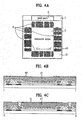
- FIGs. 4A to 4C illustrate a plane view and cross-sectional views of an active matrix electroluminescence device according to a fourth embodiment of the present invention.
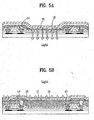
- FIGs. 5A and 5B illustrate cross-sectional views of the active matrix electroluminescence device according to the present invention.
- FIGs. 1A to 1C illustrate a plane view and cross-sectional views of an active matrix electroluminescence device according to a first embodiment of the present invention.
- a pad part 2, an emissive area 3, and a circuit part 8 are formed on a substrate 1.
- the pad part 2 is formed of a gate pad, a data pad, and so on
- the emissive area 3 is formed of a plurality of pixels.
- the circuit part 8 is formed on a non-emissive area as a gate driver or a data driver.
- the active matrix electroluminescence device also includes a metallic protective layer 10 formed on the circuit part 8 outside of the emissive area 3, so as to prevent damages caused by the UV light rays from occurring in the circuit part 8.
- the metallic protective layer 10 is formed on the area excluding the pad part 2 and the emissive area 3 of the substrate 1.
- a plurality of thin film transistors 100 and 200 are formed on a glass substrate 1.
- the thin film transistor 200 formed within the emissive area 3 acts as a switch for controlling each pixel, and the thin film transistor 100 formed outside of the emissive area 3 acts as a gate driver or a data driver.
- the thin film transistors 100 and 200 are formed of source and drain electrodes 4a and 4b, a channel area 4c, a gate insulating layer 5, and a gate electrode 6.
- an interlayer dielectric 7 is formed on the gate insulating layer 5 and the gate electrode 6. Then, the interlayer dielectric 7 and the gate insulating layer 5 are selectively etched, so as to expose a predetermined portion of the surface of the source and drain electrodes 4a and 4b, thereby forming a plurality of contact holes. The contact holes are then filled with a metal, thereby forming a plurality of electrode lines 9 each electrically connected to the source and drain electrodes 4a and 4b.
- an insulating material e.g. , a SiN x group or SiO x group material
- an insulating material e.g. , a SiN x group or SiO x group material
- the metallic protective layer 10 is formed on an area excluding the pad part 2 and the emissive area 3.
- the metallic protective layer 10 is formed on the periphery of the emissive area 3.
- a metal layer is formed on the entire surface of the protective layer 12, and then, the metallic protective layer 10 may be formed by selectively removing the metal layer on the emissive area 3 and the pad part 2.
- the metallic protective layer 10 may also be selectively deposited on the protective layer 12 by using a mask.
- the metallic protective layer 10 is formed of one of or an alloy of chrome (Cr), copper (Cu), tungsten (W), gold (Au), nickel (Ni), silver (Ag), titanium (Ti), and tantalum (Ta).
- the metallic protective layer 10 is electrically connected to the pad part 2 through a lining.
- the protective layer 12 is selectively removed, so as to expose the electrode line 9 connected to the drain electrode 4b within the emissive area 3.
- contact holes are formed in the area where the protective layer 12 is selectively removed.
- a metal is deposited on the entire surface of the protective layer 12, so as to form a pixel electrode 11.
- the pixel electrode 11 is formed of a transparent material, such as indium-tin-oxide (ITO).
- ITO indium-tin-oxide
- the pixel electrode 11 is formed of a metal having high reflectivity and work function.
- the pixel electrode 11 is formed only in the pixel area within the emissive area and is connected to the electrode line 9 within the emissive area.
- the pixel electrode 11 is formed either before forming the metallic protective layer 10, or after forming the metallic protective layer 10.
- the insulating material layer is selectively removed, so as to form an insulating layer 14 on the area excluding the pixel area, which is the boundary area between each pixel area.
- the insulating layer 14 is formed above the thin film transistor 200 of the emissive area.
- an organic electroluminous (EL) layer 15 is formed on the pixel electrode 11 by using a shadow mask (not shown), and a common electrode 16 is formed on the organic EL layer 15 and the insulating layer 14.
- a protective layer (not shown) is formed to protect the organic EL layer 15 from oxygen or moisture.
- a protective cap is formed by using a sealant and a transparent substrate.
- FIGs. 2A to 2C illustrate a plane view and cross-sectional views of the active matrix electroluminescence device according to a second embodiment of the present invention.
- a pad part 2, an emissive area 3, and a circuit part 8 are formed on a substrate 1.
- the active matrix electroluminescence device also includes a metallic protective layer 20 formed on the circuit part 8 outside of the emissive area 3, so as to prevent damages caused by the UV light rays from occurring in the circuit part 8.
- the metallic protective layer 20 is selectively formed only on the devices, such as the thin film transistor 100, which are formed outside of the emissive area 3.
- the structure of the second embodiment is the same as that of the first embodiment.
- FIGs. 3A to 3C illustrate a plane view and cross-sectional views of an active matrix electroluminescence device according to a third embodiment of the present invention.
- a pad part 2, an emissive area 3, and a circuit part 8 are formed on a substrate 1.
- the active matrix electroluminescence device also includes a metallic protective layer 30 formed on the circuit part 8 outside of the emissive area 3, so as to prevent damages caused by the UV light rays from occurring in the circuit part 8.
- the metallic protective layer 30 is formed only on a region outside of the pad part 2 and the emissive area 3.
- a plurality of thin film transistors 100 and 200 is formed on the glass substrate 41.
- the thin film transistor 200 formed within the emissive area 3 acts as a switch for controlling each pixel, and the thin film transistor 100 formed outside of the emissive area 3 acts as a gate driver or a data driver.
- the thin film transistors 100 and 200 are formed of source and drain electrodes 4a and 4b, a channel area 4c, a gate insulating layer 5, and a gate electrode 6.
- an interlayer dielectric 7 is formed on the gate insulating layer 5 and the gate electrode 6. Then, the interlayer dielectric 7 and the gate insulating layer 5 are selectively etched, so as to expose a predetermined portion of the surface of the source and drain electrodes 4a and 4b, thereby forming a plurality of contact holes. The contact holes are then filled with a metal, thereby forming a plurality of electrode lines 9 each electrically connected to the source and drain electrodes 4a and 4b.
- an insulating material e.g ., a SiN x group or SiO x group material
- a planarization overcoat 17 is formed on the protective layer 12.
- a metallic material layer is deposited on the planarization overcoat 17, and the metallic material layer is selectively removed, so as to simultaneously form the pixel electrode 11 and the metallic protective layer 30 of the same material.
- the pixel electrode 11 is formed only on the pixel area within the emissive area 3 and is connected to the electrode line 7 within the emissive area 3.
- the metallic protective layer 30 is formed in the area excluding the emissive area 3 and the pad part 2, as shown in FIG. 3A . More specifically, the metallic protective layer 30 is formed on the periphery of the emissive area 3.
- the pixel electrode 11 and the metallic protective layer 30 are formed of one of or an alloy of chrome (Cr), copper (Cu), tungsten (W), gold (Au), nickel (Ni), silver (Ag), titanium (Ti), and tantalum (Ta).
- the metallic protective layer 30 is electrically connected to the pad part 2 through a lining.
- the insulating material layer is selectively removed, so as to form an insulating layer 14 on the area excluding the pixel area, which is the boundary area between each pixel area.
- an organic electroluminous (EL) layer 15 is formed on the pixel electrode 11 by using a shadow mask (not shown), and a common electrode 16 is formed on the organic EL layer 15 and the insulating layer 14.
- FIGs. 4A to 4C illustrate a plane view and cross-sectional views of an active matrix electroluminescence device according to a fourth embodiment of the present invention.
- a pad part 2, an emissive area 3, and a circuit part 8 are formed on a substrate 1.
- the active matrix electroluminescence device also includes a metallic protective layer 40 formed on the circuit part 8 outside of the emissive area 3, so as to prevent damages caused by the UV light rays from occurring in the circuit part 8.
- the metallic protective layer 40 is selectively formed only on the devices, such as the thin film transistor 100, which are formed outside of the emissive area 3.
- the metallic protective layer 40 is formed of the same material as that of the pixel electrode 11.
- the structure of the fourth embodiment is the same as that of the third embodiment.
- the metallic protective layer is formed on devices outside of the emissive area, such as the thin film transistor, so as to prevent damage caused by the UV light rays from occurring during the fabrication process, thereby providing a highly reliable device.
Landscapes
- Engineering & Computer Science (AREA)
- Microelectronics & Electronic Packaging (AREA)
- Electroluminescent Light Sources (AREA)
- Devices For Indicating Variable Information By Combining Individual Elements (AREA)
Claims (18)
- Elektrolumineszente Aktiv-Matrix-Anzeigevorrichtung, aufweisend:eine Vielzahl von Transistoren (100, 200), welche auf einem Substrat (1) gebildet sind, auf welchem ein emittierender Bereich (3) und ein nicht emittierender Bereich definiert sind;eine Isolierschicht (14), welche auf dem Substrat (1) und den Dünnschichttransistoren (100, 200) gebildet ist;eine metallische Schutzschicht (10; 20; 30; 40), welche auf der Isolierschicht (14) des nicht emittierenden Bereichs gebildet ist;eine erste Elektrode, welche auf der Isolierschicht (14) des emittierenden Bereichs (3) gebildet ist;eine elektrolumineszierende Schicht (15), welche auf der ersten Elektrode gebildet ist; undeine zweite Elektrode, welche auf der elektrolumineszierenden Schicht (15) gebildet ist.
- Vorrichtung nach Anspruch 1, wobei die metallische Schutzschicht (10; 20; 30; 40) auf einem vorbestimmten Bereich der Isolierschicht (14) gebildet ist, die auf den Dünnschichttransistoren (100) des nicht emittierenden Bereichs gebildet ist.
- Vorrichtung nach Anspruch 1 oder 2, wobei die metallische Schutzschicht (10; 20; 30; 40) und die erste Elektrode aus dem gleichen Material gebildet sind.
- Vorrichtung nach Anspruch 3, wobei die metallische Schutzschicht (10; 20; 30; 40) und die erste Elektrode aus mindestens einem aus Chrom (Cr), Kupfer (Cu), Wolfram (W), Gold (Au), Nickel (Ni), Silber (Ag), Titan (Ti) und Tantal (Ta) gebildet sind.
- Vorrichtung nach Anspruch 1 oder 2, wobei die metallische Schutzschicht (10; 20; 30; 40) und die erste Elektrode aus unterschiedlichen Materialien gebildet sind.
- Vorrichtung nach Anspruch 5, wobei die metallische Schutzschicht (10; 20; 30; 40) aus einem undurchsichtigen Metall gebildet ist und die erste Elektrode aus einem transparenten Metall gebildet ist.
- Vorrichtung nach einem der vorhergehenden Ansprüche, wobei die metallische Schutzschicht (10; 20; 30; 40) elektrisch mit einer Gate-Anschlussstelle oder einer Datenanschlussstelle verbunden ist.
- Vorrichtung nach einem der vorhergehenden Ansprüche, wobei die erste Elektrode mit dem Dünnschichttransistor (200) des emittierenden Bereichs (3) durch ein Kontaktloch verbunden ist, das durch die Isolierschicht (14) hindurch verläuft.
- Vorrichtung nach einem der vorhergehenden Ansprüche, ferner aufweisend eine Isolierschicht (14) auf dem vorbestimmten Bereich der Isolierschicht (14) und der ersten Elektrode, die auf den Dünnschichttransistoren (200) des emittierenden Bereichs gebildet ist.
- Verfahren zur Herstellung einer elektrolumineszenten Aktiv-Matrix-Anzeigevorrichtung, aufweisend:Bilden einer Mehrzahl von Transistoren (100, 200) auf einem Substrat (1) mit einem darauf definierten emittierenden Bereich (3) und einem nicht emittierenden Bereich;Bilden einer Isolierschicht (14) auf dem Substrat und den Dünnschichttransistoren (100; 200);Bilden einer metallischen Schutzschicht (10; 20; 30; 40) auf der Isolierschicht (14) des nicht emittierenden Bereichs, und Bilden einer ersten Elektrode auf der Isolierschicht (14) des emittierenden Bereichs (3);Bilden einer elektrolumineszierenden Schicht (15) auf der ersten Elektrode; undBilden einer zweiten Elektrode auf der elektrolumineszierenden Schicht (15).
- Verfahren nach Anspruch 10, wobei eine metallische Materialschicht auf einer gesamten Oberfläche der Isolierschicht (14) gebildet ist, wobei die metallische Materialschicht dann selektiv entfernt wird, um so gleichzeitig die erste Elektrode und die metallische Schutzschicht (10; 20; 30; 40) zu bilden.
- Verfahren nach Anspruch 10 oder 11, wobei die metallische Schutzschicht (10; 20; 30; 40) aus mindestens einem aus Chrom (Cr), Kupfer (Cu), Wolfram (W), Gold (Au), Nickel (Ni), Silber (Ag), Titan (Ti) und Tantal (Ta) gebildet ist.
- Verfahren nach einem der Ansprüche 10 bis 12, wobei die metallische Schutzschicht (10; 20; 30; 40) auf einem vorbestimmten Bereich der Isolierschicht (14) gebildet ist, welche auf den Dünnschichttransistoren (100) des nicht emittierenden Bereichs gebildet ist.
- Verfahren nach einem der Ansprüche 10 bis 13, wobei die metallische Schutzschicht (10; 20; 30; 40) elektrisch mit einer Gate-Anschlusstelle oder einer Daten-Anschlussstelle verbunden ist.
- Verfahren nach einem der Ansprüche 10 bis 14, ferner aufweisend das Bilden eines Kontaktloches, das durch die Isolierschicht (14) hindurch verläuft, um so einen Teil des Dünnschichttransistors (200) in dem emittierenden Bereich (3) freizulegen.
- Verfahren nach einem der Ansprüche 10 bis 15, ferner aufweisend das Bilden einer Isolierschicht (14) auf dem vorbestimmten Bereich der Isolierschicht (14) und der ersten Elektrode auf den Dünnschichttransistoren (200) des emittierenden Bereichs (3).
- Verfahren nach einem der Ansprüche 10 bis 16, wobei die erste Elektrode aus einem transparenten Metall gebildet ist.
- Verfahren nach einem der Ansprüche 19 bis 16, wobei die metallische Schutzschicht (10; 20; 30; 40) aus einem undurchsichtigen Metall gebildet ist.
Applications Claiming Priority (2)
| Application Number | Priority Date | Filing Date | Title |
|---|---|---|---|
| KR10-2003-0040712A KR100531294B1 (ko) | 2003-06-23 | 2003-06-23 | 유기 el 소자 및 그 제조 방법 |
| KR2003040712 | 2003-06-23 |
Publications (3)
| Publication Number | Publication Date |
|---|---|
| EP1492388A2 EP1492388A2 (de) | 2004-12-29 |
| EP1492388A3 EP1492388A3 (de) | 2006-04-05 |
| EP1492388B1 true EP1492388B1 (de) | 2008-08-06 |
Family
ID=33411776
Family Applications (1)
| Application Number | Title | Priority Date | Filing Date |
|---|---|---|---|
| EP04012054A Expired - Lifetime EP1492388B1 (de) | 2003-06-23 | 2004-05-21 | Elektrolumineszente aktiv-Matrix-Vorrichtung und deren Herstellungsmethode |
Country Status (6)
| Country | Link |
|---|---|
| US (4) | US7187122B2 (de) |
| EP (1) | EP1492388B1 (de) |
| JP (1) | JP4614051B2 (de) |
| KR (1) | KR100531294B1 (de) |
| CN (1) | CN100474652C (de) |
| DE (1) | DE602004015534D1 (de) |
Families Citing this family (13)
| Publication number | Priority date | Publication date | Assignee | Title |
|---|---|---|---|---|
| KR100989252B1 (ko) * | 2003-12-29 | 2010-10-20 | 엘지디스플레이 주식회사 | 유기전계발광 소자 |
| KR101087567B1 (ko) * | 2004-03-23 | 2011-11-28 | 엘지디스플레이 주식회사 | 유기전계발광 소자 및 그 제조방법 |
| US8148895B2 (en) | 2004-10-01 | 2012-04-03 | Semiconductor Energy Laboratory Co., Ltd. | Display device and manufacturing method of the same |
| KR100821068B1 (ko) | 2006-05-16 | 2008-04-10 | 삼성에스디아이 주식회사 | 유기 전계 발광 표시 장치 및 그 제조방법 |
| KR100746983B1 (ko) * | 2006-06-29 | 2007-08-07 | 주식회사 대우일렉트로닉스 | 유기 발광 소자 패널 |
| JP4298726B2 (ja) * | 2006-07-07 | 2009-07-22 | 東芝松下ディスプレイテクノロジー株式会社 | 表示装置 |
| KR100770127B1 (ko) * | 2006-11-10 | 2007-10-24 | 삼성에스디아이 주식회사 | 유기 전계 발광 표시 장치 및 그 제조 방법 |
| KR20080099541A (ko) * | 2007-05-09 | 2008-11-13 | 삼성전자주식회사 | 표시 장치 및 그 제조 방법 |
| JP5439837B2 (ja) | 2009-02-10 | 2014-03-12 | ソニー株式会社 | 表示装置 |
| WO2012014759A1 (en) | 2010-07-26 | 2012-02-02 | Semiconductor Energy Laboratory Co., Ltd. | Light-emitting device, lighting device, and manufacturing method of light-emitting device |
| KR102032962B1 (ko) | 2012-10-26 | 2019-10-17 | 삼성디스플레이 주식회사 | 박막 트랜지스터 표시판 및 그 제조 방법 |
| CN104701337B (zh) * | 2013-12-04 | 2018-04-10 | 群创光电股份有限公司 | 主动矩阵电致发光显示装置 |
| CN114156280B (zh) * | 2021-11-29 | 2023-08-01 | 武汉华星光电半导体显示技术有限公司 | 一种显示面板及其制备方法、移动终端 |
Family Cites Families (24)
| Publication number | Priority date | Publication date | Assignee | Title |
|---|---|---|---|---|
| US3988823A (en) | 1974-08-26 | 1976-11-02 | Hughes Aircraft Company | Method for fabrication of multilayer interconnected microelectronic devices having small vias therein |
| CA1207421A (en) | 1983-11-14 | 1986-07-08 | Ottilia F. Toth | High efficiency stable cds cu.sub.2s solar cells manufacturing process using thick film methodology |
| US4637028A (en) | 1984-08-02 | 1987-01-13 | Hughes Aircraft Company | Conductively cooled laser rod |
| JP2588931B2 (ja) | 1988-05-16 | 1997-03-12 | 三菱電機株式会社 | 固体レーザ |
| JP3155132B2 (ja) | 1993-09-24 | 2001-04-09 | 三菱電機株式会社 | 固体レーザ装置及びレーザ加工装置 |
| JPH07211976A (ja) | 1994-01-24 | 1995-08-11 | Sony Corp | 光学共振器 |
| US5796766A (en) | 1994-08-23 | 1998-08-18 | Laser Power Corporation | Optically transparent heat sink for longitudinally cooling an element in a laser |
| US6101201A (en) | 1996-10-21 | 2000-08-08 | Melles Griot, Inc. | Solid state laser with longitudinal cooling |
| TW540251B (en) * | 1999-09-24 | 2003-07-01 | Semiconductor Energy Lab | EL display device and method for driving the same |
| JP3409764B2 (ja) * | 1999-12-28 | 2003-05-26 | 日本電気株式会社 | 有機el表示パネルの製造方法 |
| JP2002108250A (ja) * | 2000-09-29 | 2002-04-10 | Sharp Corp | アクティブマトリックス駆動型自発光表示装置及びその製造方法 |
| US6625193B2 (en) | 2001-01-22 | 2003-09-23 | The Boeing Company | Side-pumped active mirror solid-state laser for high-average power |
| KR200257242Y1 (ko) * | 2001-09-13 | 2001-12-22 | 엘지.필립스 엘시디 주식회사 | 유기전계발광소자 |
| JP4634673B2 (ja) * | 2001-09-26 | 2011-02-16 | シャープ株式会社 | 液晶表示装置及びその製造方法 |
| KR100563131B1 (ko) * | 2001-11-05 | 2006-03-21 | 엘지.필립스 엘시디 주식회사 | 유기전계발광 소자 |
| JP3617644B2 (ja) | 2002-03-26 | 2005-02-09 | ソニー株式会社 | 液体吐出装置 |
| TW595254B (en) * | 2002-03-29 | 2004-06-21 | Sanyo Electric Co | Electroluminescense display device |
| TW591564B (en) * | 2002-04-24 | 2004-06-11 | Sanyo Electric Co | Display device |
| JP2003316284A (ja) * | 2002-04-24 | 2003-11-07 | Sanyo Electric Co Ltd | 表示装置 |
| TWI227654B (en) * | 2002-04-26 | 2005-02-01 | Sanyo Electric Co | Method for dimming an electroluminescence display panel, and electroluminescence display panel |
| JP2003332045A (ja) * | 2002-05-09 | 2003-11-21 | Sanyo Electric Co Ltd | エレクトロルミネッセンス表示装置及びその製造方法 |
| JP4281293B2 (ja) * | 2002-05-10 | 2009-06-17 | セイコーエプソン株式会社 | 電気光学装置の製造方法及び電気光学装置の製造装置 |
| JP3884351B2 (ja) * | 2002-08-26 | 2007-02-21 | 株式会社 日立ディスプレイズ | 画像表示装置およびその製造方法 |
| JP2004101948A (ja) * | 2002-09-10 | 2004-04-02 | Dainippon Printing Co Ltd | 表示装置およびその製造方法 |
-
2003
- 2003-06-23 KR KR10-2003-0040712A patent/KR100531294B1/ko not_active Expired - Fee Related
-
2004
- 2004-05-03 US US10/836,348 patent/US7187122B2/en not_active Expired - Fee Related
- 2004-05-21 DE DE602004015534T patent/DE602004015534D1/de not_active Expired - Lifetime
- 2004-05-21 EP EP04012054A patent/EP1492388B1/de not_active Expired - Lifetime
- 2004-05-24 CN CNB2004100383823A patent/CN100474652C/zh not_active Expired - Fee Related
- 2004-06-14 JP JP2004175628A patent/JP4614051B2/ja not_active Expired - Fee Related
-
2007
- 2007-01-23 US US11/656,471 patent/US7755280B2/en not_active Expired - Lifetime
- 2007-09-13 US US11/854,700 patent/US7876040B2/en not_active Expired - Lifetime
-
2010
- 2010-12-16 US US12/970,356 patent/US8344620B2/en not_active Expired - Fee Related
Also Published As
| Publication number | Publication date |
|---|---|
| EP1492388A2 (de) | 2004-12-29 |
| JP2005019401A (ja) | 2005-01-20 |
| US20040256985A1 (en) | 2004-12-23 |
| DE602004015534D1 (de) | 2008-09-18 |
| US20110089813A1 (en) | 2011-04-21 |
| EP1492388A3 (de) | 2006-04-05 |
| US7187122B2 (en) | 2007-03-06 |
| CN1575060A (zh) | 2005-02-02 |
| US7755280B2 (en) | 2010-07-13 |
| US20070131943A1 (en) | 2007-06-14 |
| KR20050000130A (ko) | 2005-01-03 |
| CN100474652C (zh) | 2009-04-01 |
| KR100531294B1 (ko) | 2005-11-28 |
| US7876040B2 (en) | 2011-01-25 |
| US8344620B2 (en) | 2013-01-01 |
| US20080174240A1 (en) | 2008-07-24 |
| JP4614051B2 (ja) | 2011-01-19 |
Similar Documents
| Publication | Publication Date | Title |
|---|---|---|
| US7755280B2 (en) | Active matrix electroluminescence device having a metallic protective layer and method for fabricating the same | |
| US7312571B2 (en) | Organic electroluminescent device including layer having uneven patterns | |
| US8937311B2 (en) | Thin film transistor, thin film transistor array substrate and method of fabricating the same | |
| US8987725B2 (en) | Flat panel display device | |
| US7803029B2 (en) | Method of fabricating organic electroluminescent display device | |
| US12342624B2 (en) | Display apparatus | |
| US9570529B2 (en) | Organic light emitting diode display | |
| US20040032202A1 (en) | Luminescent apparatus and method of manufacturing the same | |
| US20110220898A1 (en) | Organic light emitting diode display and manufacturing method thereof | |
| EP1505666A2 (de) | Nach oben abstrahlende elektrolumineszente Vorrichtung mit aktiver Matrix und Verfahren zu deren Herstellung | |
| JP4488557B2 (ja) | El表示装置 | |
| US8310151B2 (en) | Active matrix electroluminescence device and method for fabricating the same | |
| CN112186004A (zh) | 显示设备 | |
| US12063846B2 (en) | Display device capable of preventing burnt | |
| KR20230102327A (ko) | 표시 장치 및 그의 제조 방법 |
Legal Events
| Date | Code | Title | Description |
|---|---|---|---|
| PUAI | Public reference made under article 153(3) epc to a published international application that has entered the european phase |
Free format text: ORIGINAL CODE: 0009012 |
|
| AK | Designated contracting states |
Kind code of ref document: A2 Designated state(s): AT BE BG CH CY CZ DE DK EE ES FI FR GB GR HU IE IT LI LU MC NL PL PT RO SE SI SK TR |
|
| AX | Request for extension of the european patent |
Extension state: AL HR LT LV MK |
|
| PUAL | Search report despatched |
Free format text: ORIGINAL CODE: 0009013 |
|
| AK | Designated contracting states |
Kind code of ref document: A3 Designated state(s): AT BE BG CH CY CZ DE DK EE ES FI FR GB GR HU IE IT LI LU MC NL PL PT RO SE SI SK TR |
|
| AX | Request for extension of the european patent |
Extension state: AL HR LT LV MK |
|
| RIC1 | Information provided on ipc code assigned before grant |
Ipc: H01L 23/552 20060101AFI20060215BHEP |
|
| 17P | Request for examination filed |
Effective date: 20060729 |
|
| 17Q | First examination report despatched |
Effective date: 20060905 |
|
| AKX | Designation fees paid |
Designated state(s): DE FR GB NL |
|
| GRAP | Despatch of communication of intention to grant a patent |
Free format text: ORIGINAL CODE: EPIDOSNIGR1 |
|
| GRAS | Grant fee paid |
Free format text: ORIGINAL CODE: EPIDOSNIGR3 |
|
| GRAA | (expected) grant |
Free format text: ORIGINAL CODE: 0009210 |
|
| AK | Designated contracting states |
Kind code of ref document: B1 Designated state(s): DE FR GB NL |
|
| REG | Reference to a national code |
Ref country code: GB Ref legal event code: FG4D |
|
| REF | Corresponds to: |
Ref document number: 602004015534 Country of ref document: DE Date of ref document: 20080918 Kind code of ref document: P |
|
| PG25 | Lapsed in a contracting state [announced via postgrant information from national office to epo] |
Ref country code: NL Free format text: LAPSE BECAUSE OF FAILURE TO SUBMIT A TRANSLATION OF THE DESCRIPTION OR TO PAY THE FEE WITHIN THE PRESCRIBED TIME-LIMIT Effective date: 20080806 |
|
| PLBE | No opposition filed within time limit |
Free format text: ORIGINAL CODE: 0009261 |
|
| STAA | Information on the status of an ep patent application or granted ep patent |
Free format text: STATUS: NO OPPOSITION FILED WITHIN TIME LIMIT |
|
| 26N | No opposition filed |
Effective date: 20090507 |
|
| REG | Reference to a national code |
Ref country code: FR Ref legal event code: PLFP Year of fee payment: 13 |
|
| REG | Reference to a national code |
Ref country code: FR Ref legal event code: PLFP Year of fee payment: 14 |
|
| REG | Reference to a national code |
Ref country code: FR Ref legal event code: PLFP Year of fee payment: 15 |
|
| PGFP | Annual fee paid to national office [announced via postgrant information from national office to epo] |
Ref country code: DE Payment date: 20200406 Year of fee payment: 17 Ref country code: FR Payment date: 20200408 Year of fee payment: 17 |
|
| PGFP | Annual fee paid to national office [announced via postgrant information from national office to epo] |
Ref country code: GB Payment date: 20200408 Year of fee payment: 17 |
|
| REG | Reference to a national code |
Ref country code: DE Ref legal event code: R119 Ref document number: 602004015534 Country of ref document: DE |
|
| GBPC | Gb: european patent ceased through non-payment of renewal fee |
Effective date: 20210521 |
|
| PG25 | Lapsed in a contracting state [announced via postgrant information from national office to epo] |
Ref country code: GB Free format text: LAPSE BECAUSE OF NON-PAYMENT OF DUE FEES Effective date: 20210521 Ref country code: DE Free format text: LAPSE BECAUSE OF NON-PAYMENT OF DUE FEES Effective date: 20211201 |
|
| PG25 | Lapsed in a contracting state [announced via postgrant information from national office to epo] |
Ref country code: FR Free format text: LAPSE BECAUSE OF NON-PAYMENT OF DUE FEES Effective date: 20210531 |