EP1493711B1 - Herstellungsverfahren für eine Halbleitervorrichtung mit einem hängenden Mikrosystem und entsprechende Vorrichtung - Google Patents
Herstellungsverfahren für eine Halbleitervorrichtung mit einem hängenden Mikrosystem und entsprechende Vorrichtung Download PDFInfo
- Publication number
- EP1493711B1 EP1493711B1 EP03425441A EP03425441A EP1493711B1 EP 1493711 B1 EP1493711 B1 EP 1493711B1 EP 03425441 A EP03425441 A EP 03425441A EP 03425441 A EP03425441 A EP 03425441A EP 1493711 B1 EP1493711 B1 EP 1493711B1
- Authority
- EP
- European Patent Office
- Prior art keywords
- layer
- polysilicon layer
- polysilicon
- semiconductor device
- porous
- Prior art date
- Legal status (The legal status is an assumption and is not a legal conclusion. Google has not performed a legal analysis and makes no representation as to the accuracy of the status listed.)
- Expired - Lifetime
Links
Images


Classifications
-
- B—PERFORMING OPERATIONS; TRANSPORTING
- B81—MICROSTRUCTURAL TECHNOLOGY
- B81C—PROCESSES OR APPARATUS SPECIALLY ADAPTED FOR THE MANUFACTURE OR TREATMENT OF MICROSTRUCTURAL DEVICES OR SYSTEMS
- B81C1/00—Manufacture or treatment of devices or systems in or on a substrate
- B81C1/00015—Manufacture or treatment of devices or systems in or on a substrate for manufacturing microsystems
- B81C1/00134—Manufacture or treatment of devices or systems in or on a substrate for manufacturing microsystems comprising flexible or deformable structures
- B81C1/00142—Bridges
-
- B—PERFORMING OPERATIONS; TRANSPORTING
- B81—MICROSTRUCTURAL TECHNOLOGY
- B81B—MICROSTRUCTURAL DEVICES OR SYSTEMS, e.g. MICROMECHANICAL DEVICES
- B81B2201/00—Specific applications of microelectromechanical systems
- B81B2201/04—Optical MEMS
- B81B2201/042—Micromirrors, not used as optical switches
-
- B—PERFORMING OPERATIONS; TRANSPORTING
- B81—MICROSTRUCTURAL TECHNOLOGY
- B81C—PROCESSES OR APPARATUS SPECIALLY ADAPTED FOR THE MANUFACTURE OR TREATMENT OF MICROSTRUCTURAL DEVICES OR SYSTEMS
- B81C2201/00—Manufacture or treatment of microstructural devices or systems
- B81C2201/01—Manufacture or treatment of microstructural devices or systems in or on a substrate
- B81C2201/0101—Shaping material; Structuring the bulk substrate or layers on the substrate; Film patterning
- B81C2201/0111—Bulk micromachining
- B81C2201/0115—Porous silicon
Definitions
- the present invention refers to a process for the obtainment of a semiconductor device comprising a suspended micro-system, to a device so obtained and its applications.
- the suspended micro-systems defined also semiconductor suspended structures, in the integrated circuits, are generally used in the case in which there is the necessity to provide orthogonal movements of portions of the surface of a crystal of silicon opportunely worked.
- micro-systems can be for example for the realization of micro minor thermally moved.
- the obtainment of such structures is a very complex process.
- the complexity is to be searched in the impossibility to realize sacrificial layers of elevated thickness, for example of about ten micrometres, with the VLSI and ULSI technologies.
- EP 0747686 discloses a method foi forming a diaphragm supported in a cavity, comprising the steps of implanting a P type layer in a substrate, depositing an n-type layer on the substrate, implanting spaced sinkers through the epitaxial layer and into electrical connection with the layer, anodising the substrate to form porous silicon of the sinkers and said layer, oxidizing said porous silicon to form silicon dioxide and etching the silicon dioxide to form the cavity and the diaphragm.
- the present invention it is possible to realize a suspended micro-system using a porous layer of silicon as sacrificial oxide and to create in this way a three-dimensional structure below the suspended micro-system, that allows the micro-system to freely move without touching structures near it
- the micro-system results suspended by hinges obtained with the same material of the micro-system that has not been removed.
- the hinges are connected to walls being formed during the obtainment of the device.
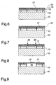
- the following step provides for the oxidation of the porous layer 11, to get an oxidized porous layer 12.
- the oxidation is obtained at low temperature, around 900 °Cs, for a brief period of 30 minutes, enough for oxidizing the thread-like structure with an average diameter of 50 nm (that can vary in accordance to the process) which constitutes the crystalline skeleton of the porous silicon.
- an average diameter of 50 nm that can vary in accordance to the process
- the following steps allow to realize some suspended structures in polysilicon by using the oxidized porous layer as sacrificial layer.
- a process of deposition and photoengraving of the resist follows. Then a plasma attack of the polysilicon layer 14, effected with a mixture of Cl 2 and HBr followed by a process at high selectivity with respect to the silicon oxide with a mixture of He, O 2 and HBr, is carried out, thereby delimiting portions of the structure as it can be seen in figure 3 .
- the two layers 16 and 17 will uniformly distribute themselves on the whole surface thereby linking to the silicon substrate.
Landscapes
- Engineering & Computer Science (AREA)
- Manufacturing & Machinery (AREA)
- Microelectronics & Electronic Packaging (AREA)
- Micromachines (AREA)
- Element Separation (AREA)
Claims (9)
- Verfahren zur Erhaltung einer Halbleitervorrichtung, die ein hängendes Mikrosystem aufweist, folgende Schritte aufweisend:Ausbilden eines Siliciumsubstrats (10);Ausbilden einer porösen Siliciumschicht (11) über dem Substrat (10);Oxidieren der porösen Schicht (12);Abscheiden einer Oxidschicht (13) auf der gesamten Vorrichtung;Abscheiden einer ersten Polysiliciumschicht (14) über der Oxidschicht (13);Entfernen der ersten Polysiliciumschicht (14), der Oxidschicht (13) und der porösen Schicht (12) an ausgewählten Stellen, um Rinnen (15) nach unten bis zum Erreichen des Substrats (10) auszubilden;Abscheiden einer Nitridschicht (16) auf der gesamten Vorrichtung;Abscheiden einer zweiten Polysiliciumschicht (17) auf der gesamten Vorrichtung, um die Rinnen (15) mit einer Doppelschicht aus Nitrid (16) und Polysilicium (17) zu füllen;Entfernen der zweiten Polysiliciumschicht (17), der Nitridschicht (16), der ersten Polysiliciumschicht (14) und der Oxidschicht (13) an ausgewählten Stellen;Entfernen der oxidierten porösen Schicht (12) in den Bereichen (18), die durch den vorangehenden Entfernungsschritt zugänglich gemacht wurden und von den gefüllten Rinnen (15) als Seitenwänden begrenzt werden.
- Verfahren nach Anspruch 1, dadurch gekennzeichnet, dass bei dem Schritt des Entfernens der ersten Polysiliciumschicht (14), der Oxidschicht (13) und der porösen Schicht (12) an ausgewählten Stellen die erste Polysiliciumschicht (14) als Maske in einem fotolithografischen Prozess verwendet wird.
- Verfahren nach Anspruch 1, dadurch gekennzeichnet, dass bei dem Schritt des Entfernens der zweiten Polysiliciumschicht (17), der Nitridschicht (16) und der ersten Polysiliciumschicht (14) an ausgewählten Stellen die zweite Polysiliciumschicht (17) als Maske in einem fotolithografischen Prozess verwendet wird.
- Verfahren nach Anspruch 1, dadurch gekennzeichnet, dass die zweite Polysiliciumschicht (17), die Nitridschicht (16) und die erste Polysiliciumschicht (14) an ausgewählten Stellen entfernt werden, um eine Hängestruktur (19), die durch gewisse nicht entfernte Teile (22, 24) der Hängestruktur (19) seitlich befestigt ist, zu schaffen.
- Halbleitervorrichtung, aufweisend ein hängendes Mikrosystem (19), das durch Gelenke (22, 24) an mindestens zwei Wänden befestigt ist, wobei die zwei Wände über einem Siliciumsubstrat (10) angebracht sind und von einer ersten Nitridschicht (16) und einer zweiten Polysiliciumschicht (17) gebildet werden, wobei das Mikrosystem (19) in Aufeinanderfolge von einer Oxidschicht (13), einer ersten Polysiliciumschicht (14), einer Nitridschicht (16) und der zweiten Polysiliciumschicht (17) aufgebaut ist, wobei die Vorrichtung unter dem Mikrosystem (19) einen leeren Raum (18) aufweist, wobei der leere Raum (18) Seitenwände hat, die aus oxidiertem porösen Silicium (12), bedeckt von der ersten Nitridschicht (16) und der zweiten Polysiliciumschicht (17), bestehen.
- Halbleitervorrichtung nach Anspruch 5, dadurch gekennzeichnet, dass die Gelenke in Aufeinanderfolge durch eine Oxidschicht (13), eine erste Polysiliciumschicht (14), eine Nitridschicht (16) und eine zweite Polysiliciumschicht (17) aufgebaut sind.
- Halbleitervorrichtung nach Anspruch 5, dadurch gekennzeichnet, dass die Gelenke (22, 24) von begrenzten Materialbereichen, die die Wände mit der Hängestruktur (19) strukturell verbinden, gebildet werden.
- Halbleitervorrichtung nach Anspruch 5, dadurch gekennzeichnet, dass das Mikrosystem (19) ein Mikrospiegel ist.
- Halbleitervorrichtung nach Anspruch 8, dadurch gekennzeichnet, dass der Mikrospiegel mittels eines Thermo-Betätigungselements (23) bewegt wird.
Priority Applications (4)
| Application Number | Priority Date | Filing Date | Title |
|---|---|---|---|
| DE60320391T DE60320391D1 (de) | 2003-07-04 | 2003-07-04 | Herstellungsverfahren für eine Halbleitervorrichtung mit einem hängenden Mikrosystem und entsprechende Vorrichtung |
| EP03425441A EP1493711B1 (de) | 2003-07-04 | 2003-07-04 | Herstellungsverfahren für eine Halbleitervorrichtung mit einem hängenden Mikrosystem und entsprechende Vorrichtung |
| US10/884,867 US7195946B2 (en) | 2003-07-04 | 2004-07-02 | Process for fabricating a semiconductor device having a suspended micro-system and resultant device |
| US11/683,785 US7777285B2 (en) | 2003-07-04 | 2007-03-08 | Semiconductor device having a suspended micro-system |
Applications Claiming Priority (1)
| Application Number | Priority Date | Filing Date | Title |
|---|---|---|---|
| EP03425441A EP1493711B1 (de) | 2003-07-04 | 2003-07-04 | Herstellungsverfahren für eine Halbleitervorrichtung mit einem hängenden Mikrosystem und entsprechende Vorrichtung |
Publications (2)
| Publication Number | Publication Date |
|---|---|
| EP1493711A1 EP1493711A1 (de) | 2005-01-05 |
| EP1493711B1 true EP1493711B1 (de) | 2008-04-16 |
Family
ID=33427300
Family Applications (1)
| Application Number | Title | Priority Date | Filing Date |
|---|---|---|---|
| EP03425441A Expired - Lifetime EP1493711B1 (de) | 2003-07-04 | 2003-07-04 | Herstellungsverfahren für eine Halbleitervorrichtung mit einem hängenden Mikrosystem und entsprechende Vorrichtung |
Country Status (3)
| Country | Link |
|---|---|
| US (2) | US7195946B2 (de) |
| EP (1) | EP1493711B1 (de) |
| DE (1) | DE60320391D1 (de) |
Cited By (2)
| Publication number | Priority date | Publication date | Assignee | Title |
|---|---|---|---|---|
| US8308962B2 (en) | 2007-09-14 | 2012-11-13 | Qualcomm Mems Technologies, Inc. | Etching processes used in MEMS production |
| US8536059B2 (en) | 2007-02-20 | 2013-09-17 | Qualcomm Mems Technologies, Inc. | Equipment and methods for etching of MEMS |
Families Citing this family (13)
| Publication number | Priority date | Publication date | Assignee | Title |
|---|---|---|---|---|
| KR100692593B1 (ko) * | 2005-01-24 | 2007-03-13 | 삼성전자주식회사 | Mems 구조체, 외팔보 형태의 mems 구조체 및밀봉된 유체채널의 제조 방법. |
| US7608470B2 (en) * | 2005-06-28 | 2009-10-27 | Intel Corporation | Interconnection device including one or more embedded vias and method of producing the same |
| JP2009503564A (ja) | 2005-07-22 | 2009-01-29 | クアルコム,インコーポレイテッド | Memsデバイスのための支持構造、およびその方法 |
| US7732241B2 (en) * | 2005-11-30 | 2010-06-08 | Semiconductor Energy Labortory Co., Ltd. | Microstructure and manufacturing method thereof and microelectromechanical system |
| DE102007015726B4 (de) * | 2007-04-02 | 2011-09-29 | Fraunhofer-Gesellschaft zur Förderung der angewandten Forschung e.V. | Auslenkbare Struktur, mikromechanische Struktur mit derselben und Verfahren zur Einstellung einer mikromechanischen Struktur |
| EP2129619A2 (de) | 2007-04-04 | 2009-12-09 | Qualcomm Mems Technologies, Inc. | Beseitigung von freisetzungsätzangriffen durch schnittstellenmodifikation in opferschichten |
| US7749789B2 (en) * | 2008-03-18 | 2010-07-06 | Solid-State Research, Inc. | CMOS-compatible bulk-micromachining process for single-crystal MEMS/NEMS devices |
| US8613816B2 (en) * | 2008-03-21 | 2013-12-24 | California Institute Of Technology | Forming of ferromagnetic metallic glass by rapid capacitor discharge |
| US8664731B2 (en) * | 2011-02-14 | 2014-03-04 | Kionix, Inc. | Strengthened micro-electromechanical system devices and methods of making thereof |
| FR3006304B1 (fr) | 2013-05-28 | 2015-07-03 | Commissariat Energie Atomique | Procede de realisation d'une partie suspendue d'une structure microelectronique et/ou nanoelectronique dans une partie monolithique d'un substrat |
| US10876903B2 (en) * | 2019-03-20 | 2020-12-29 | Xiang Zheng Tu | Multi-purpose MEMS thermopile sensors |
| US11118979B2 (en) * | 2019-09-16 | 2021-09-14 | Xiang Zheng Tu | Vacuum packaged infrared sensor arrays |
| CN112382678A (zh) * | 2020-11-13 | 2021-02-19 | 福建新峰二维材料科技有限公司 | 一种铸造单晶硅异质结太阳电池的制备方法 |
Family Cites Families (14)
| Publication number | Priority date | Publication date | Assignee | Title |
|---|---|---|---|---|
| US5090254A (en) * | 1990-04-11 | 1992-02-25 | Wisconsin Alumni Research Foundation | Polysilicon resonating beam transducers |
| US5736430A (en) * | 1995-06-07 | 1998-04-07 | Ssi Technologies, Inc. | Transducer having a silicon diaphragm and method for forming same |
| CA2176052A1 (en) * | 1995-06-07 | 1996-12-08 | James D. Seefeldt | Transducer having a resonating silicon beam and method for forming same |
| US6021675A (en) * | 1995-06-07 | 2000-02-08 | Ssi Technologies, Inc. | Resonating structure and method for forming the resonating structure |
| US6395618B2 (en) * | 1998-07-10 | 2002-05-28 | Stmicroelectronics S.R.L. | Method for manufacturing integrated structures including removing a sacrificial region |
| US6225140B1 (en) * | 1998-10-13 | 2001-05-01 | Institute Of Microelectronics | CMOS compatable surface machined pressure sensor and method of fabricating the same |
| US7083997B2 (en) * | 2000-08-03 | 2006-08-01 | Analog Devices, Inc. | Bonded wafer optical MEMS process |
| US6734762B2 (en) * | 2001-04-09 | 2004-05-11 | Motorola, Inc. | MEMS resonators and method for manufacturing MEMS resonators |
| US6736982B2 (en) * | 2001-06-15 | 2004-05-18 | Xiang Zheng Tu | Micromachined vertical vibrating gyroscope |
| ATE355530T1 (de) * | 2001-07-26 | 2006-03-15 | Fraunhofer Ges Forschung | Mikromechanisches bauelement |
| DE10244785A1 (de) * | 2002-09-26 | 2004-04-08 | Robert Bosch Gmbh | Verfahren und mikromechanisches Bauelement |
| JP4252889B2 (ja) * | 2003-08-12 | 2009-04-08 | 富士通株式会社 | マイクロ構造体の製造方法 |
| US7078337B2 (en) * | 2003-09-30 | 2006-07-18 | Agere Systems Inc. | Selective isotropic etch for titanium-based materials |
| US7115436B2 (en) * | 2004-02-12 | 2006-10-03 | Robert Bosch Gmbh | Integrated getter area for wafer level encapsulated microelectromechanical systems |
-
2003
- 2003-07-04 DE DE60320391T patent/DE60320391D1/de not_active Expired - Lifetime
- 2003-07-04 EP EP03425441A patent/EP1493711B1/de not_active Expired - Lifetime
-
2004
- 2004-07-02 US US10/884,867 patent/US7195946B2/en not_active Expired - Fee Related
-
2007
- 2007-03-08 US US11/683,785 patent/US7777285B2/en not_active Expired - Lifetime
Cited By (3)
| Publication number | Priority date | Publication date | Assignee | Title |
|---|---|---|---|---|
| US8536059B2 (en) | 2007-02-20 | 2013-09-17 | Qualcomm Mems Technologies, Inc. | Equipment and methods for etching of MEMS |
| US8308962B2 (en) | 2007-09-14 | 2012-11-13 | Qualcomm Mems Technologies, Inc. | Etching processes used in MEMS production |
| US8323516B2 (en) | 2007-09-14 | 2012-12-04 | Qualcomm Mems Technologies, Inc. | Etching processes used in MEMS production |
Also Published As
| Publication number | Publication date |
|---|---|
| US20050026321A1 (en) | 2005-02-03 |
| US7195946B2 (en) | 2007-03-27 |
| US7777285B2 (en) | 2010-08-17 |
| US20070145501A1 (en) | 2007-06-28 |
| EP1493711A1 (de) | 2005-01-05 |
| DE60320391D1 (de) | 2008-05-29 |
Similar Documents
| Publication | Publication Date | Title |
|---|---|---|
| US7777285B2 (en) | Semiconductor device having a suspended micro-system | |
| EP1417151B9 (de) | Verfahren zur herstellung aufgehängter poröser siliziummikrostrukturen und anwendung in gassensoren | |
| JP5221845B2 (ja) | トレンチされたキャビティを有するセンサエレメント | |
| US7276277B2 (en) | Micromechanical component, in particular a sensor element, having a stabilized membrane and a method of producing such a component | |
| JP4431502B2 (ja) | エピタキシによって半導体デバイスを形成する方法 | |
| US8716052B2 (en) | Method for making a structure comprising at least one multi-thick active part | |
| JP2004502555A (ja) | 半導体構成素子の製造方法並びにその方法により製造された半導体構成素子 | |
| JP2004209640A (ja) | エピタキシャルリアクタにおける表面マイクロマシニングされた構造のためのギャップチューニング | |
| US7456041B2 (en) | Manufacturing method of a MEMS structure, a cantilever-type MEMS structure, and a sealed fluidic channel | |
| JP2010017843A (ja) | 部分的な単結晶アンカーを含むmems/nems構造体及びその製造方法 | |
| Kaltsas et al. | Bulk silicon micromachining using porous silicon sacrificial layers | |
| French et al. | New silicon micromachining techniques for microsystems | |
| US7755152B2 (en) | Semiconductor component configured as a diaphragm sensor | |
| JP4327456B2 (ja) | マイクロメカニックス構成素子及びその製造方法 | |
| Serry et al. | Silicon Germanium as a novel mask for silicon deep reactive ion etching | |
| US20030199148A1 (en) | Method of reducing the thickness of a silicon substrate | |
| US7803646B2 (en) | Method for producing a component having a semiconductor substrate and component | |
| Kuhl et al. | Formation of porous silicon using an ammonium fluoride based electrolyte for application as a sacrificial layer | |
| US8501516B2 (en) | Method for producing micromechanical patterns having a relief-like sidewall outline shape or an adjustable angle of inclination | |
| US20060115919A1 (en) | Method of making a microelectromechanical (MEM) device using porous material as a sacrificial layer | |
| Zorman et al. | Advanced processing techniques for silicon carbide MEMS and NEMS | |
| Rao et al. | Microstructures with protected convex corners in modified KOH solution exhibiting high-speed silicon etching | |
| Kaltsas et al. | The proposed process is fully C-MOS compatible and it was successfully used to fabricate deep cavities into silicon with very smooth bottom surfaces and sidewalls. Suspended flat polysilicon membranes were also produced of a surface as large as 230 x 550 pum?, as well as polysilicon cantilevers. This process opens important possibilities in silicon integrated sensor fabrication. | |
| He et al. | Post-deposition porous etching of polysilicon: Fabrication and characterization of free-standing structures | |
| Yue et al. | Porous Silicon Fabrication Process for Optical Reflectors |
Legal Events
| Date | Code | Title | Description |
|---|---|---|---|
| PUAI | Public reference made under article 153(3) epc to a published international application that has entered the european phase |
Free format text: ORIGINAL CODE: 0009012 |
|
| AK | Designated contracting states |
Kind code of ref document: A1 Designated state(s): AT BE BG CH CY CZ DE DK EE ES FI FR GB GR HU IE IT LI LU MC NL PT RO SE SI SK TR |
|
| AX | Request for extension of the european patent |
Extension state: AL LT LV MK |
|
| 17P | Request for examination filed |
Effective date: 20050613 |
|
| AKX | Designation fees paid |
Designated state(s): DE FR GB IT |
|
| 17Q | First examination report despatched |
Effective date: 20050715 |
|
| GRAP | Despatch of communication of intention to grant a patent |
Free format text: ORIGINAL CODE: EPIDOSNIGR1 |
|
| GRAS | Grant fee paid |
Free format text: ORIGINAL CODE: EPIDOSNIGR3 |
|
| GRAA | (expected) grant |
Free format text: ORIGINAL CODE: 0009210 |
|
| AK | Designated contracting states |
Kind code of ref document: B1 Designated state(s): DE FR GB IT |
|
| REF | Corresponds to: |
Ref document number: 60320391 Country of ref document: DE Date of ref document: 20080529 Kind code of ref document: P |
|
| ET | Fr: translation filed | ||
| PLBE | No opposition filed within time limit |
Free format text: ORIGINAL CODE: 0009261 |
|
| STAA | Information on the status of an ep patent application or granted ep patent |
Free format text: STATUS: NO OPPOSITION FILED WITHIN TIME LIMIT |
|
| 26N | No opposition filed |
Effective date: 20090119 |
|
| GBPC | Gb: european patent ceased through non-payment of renewal fee |
Effective date: 20080716 |
|
| PG25 | Lapsed in a contracting state [announced via postgrant information from national office to epo] |
Ref country code: DE Free format text: LAPSE BECAUSE OF FAILURE TO SUBMIT A TRANSLATION OF THE DESCRIPTION OR TO PAY THE FEE WITHIN THE PRESCRIBED TIME-LIMIT Effective date: 20080717 |
|
| PG25 | Lapsed in a contracting state [announced via postgrant information from national office to epo] |
Ref country code: GB Free format text: LAPSE BECAUSE OF NON-PAYMENT OF DUE FEES Effective date: 20080716 |
|
| PGFP | Annual fee paid to national office [announced via postgrant information from national office to epo] |
Ref country code: FR Payment date: 20110810 Year of fee payment: 9 |
|
| PGFP | Annual fee paid to national office [announced via postgrant information from national office to epo] |
Ref country code: IT Payment date: 20120626 Year of fee payment: 10 |
|
| REG | Reference to a national code |
Ref country code: FR Ref legal event code: ST Effective date: 20130329 |
|
| PG25 | Lapsed in a contracting state [announced via postgrant information from national office to epo] |
Ref country code: FR Free format text: LAPSE BECAUSE OF NON-PAYMENT OF DUE FEES Effective date: 20120731 |
|
| PG25 | Lapsed in a contracting state [announced via postgrant information from national office to epo] |
Ref country code: IT Free format text: LAPSE BECAUSE OF NON-PAYMENT OF DUE FEES Effective date: 20130704 |