EP1494078A1 - Lithographischer Apparat und Verfahren zur Herstellung einer Vorrichtung - Google Patents
Lithographischer Apparat und Verfahren zur Herstellung einer Vorrichtung Download PDFInfo
- Publication number
- EP1494078A1 EP1494078A1 EP04076864A EP04076864A EP1494078A1 EP 1494078 A1 EP1494078 A1 EP 1494078A1 EP 04076864 A EP04076864 A EP 04076864A EP 04076864 A EP04076864 A EP 04076864A EP 1494078 A1 EP1494078 A1 EP 1494078A1
- Authority
- EP
- European Patent Office
- Prior art keywords
- substrate
- correction signal
- movable part
- movable
- movable parts
- Prior art date
- Legal status (The legal status is an assumption and is not a legal conclusion. Google has not performed a legal analysis and makes no representation as to the accuracy of the status listed.)
- Withdrawn
Links
- 238000004519 manufacturing process Methods 0.000 title claims description 15
- 239000000758 substrate Substances 0.000 claims abstract description 123
- 238000005259 measurement Methods 0.000 claims abstract description 69
- 238000006073 displacement reaction Methods 0.000 claims abstract description 21
- 238000012937 correction Methods 0.000 claims description 105
- 230000005855 radiation Effects 0.000 claims description 38
- 230000001133 acceleration Effects 0.000 claims description 28
- 238000000059 patterning Methods 0.000 claims description 17
- 239000000463 material Substances 0.000 claims description 10
- 230000003287 optical effect Effects 0.000 claims description 8
- 239000010410 layer Substances 0.000 description 15
- 238000000034 method Methods 0.000 description 13
- 235000012431 wafers Nutrition 0.000 description 6
- 230000000694 effects Effects 0.000 description 5
- 238000012545 processing Methods 0.000 description 4
- 238000003491 array Methods 0.000 description 2
- 238000001514 detection method Methods 0.000 description 2
- 230000006870 function Effects 0.000 description 2
- 239000011159 matrix material Substances 0.000 description 2
- 230000010363 phase shift Effects 0.000 description 2
- 230000008569 process Effects 0.000 description 2
- 239000004065 semiconductor Substances 0.000 description 2
- XUIMIQQOPSSXEZ-UHFFFAOYSA-N Silicon Chemical compound [Si] XUIMIQQOPSSXEZ-UHFFFAOYSA-N 0.000 description 1
- 238000010521 absorption reaction Methods 0.000 description 1
- 230000002411 adverse Effects 0.000 description 1
- 230000002238 attenuated effect Effects 0.000 description 1
- 230000033228 biological regulation Effects 0.000 description 1
- 230000005540 biological transmission Effects 0.000 description 1
- 230000008859 change Effects 0.000 description 1
- 239000011248 coating agent Substances 0.000 description 1
- 238000000576 coating method Methods 0.000 description 1
- 238000010276 construction Methods 0.000 description 1
- 230000007423 decrease Effects 0.000 description 1
- 230000001934 delay Effects 0.000 description 1
- 238000013461 design Methods 0.000 description 1
- 238000011161 development Methods 0.000 description 1
- 238000010586 diagram Methods 0.000 description 1
- 230000004069 differentiation Effects 0.000 description 1
- 230000009977 dual effect Effects 0.000 description 1
- 230000005684 electric field Effects 0.000 description 1
- 230000005670 electromagnetic radiation Effects 0.000 description 1
- 238000010894 electron beam technology Methods 0.000 description 1
- 238000005530 etching Methods 0.000 description 1
- 238000003384 imaging method Methods 0.000 description 1
- 238000007689 inspection Methods 0.000 description 1
- 230000010354 integration Effects 0.000 description 1
- 238000005468 ion implantation Methods 0.000 description 1
- 238000010884 ion-beam technique Methods 0.000 description 1
- 239000002346 layers by function Substances 0.000 description 1
- 239000004973 liquid crystal related substance Substances 0.000 description 1
- 238000001459 lithography Methods 0.000 description 1
- 230000005381 magnetic domain Effects 0.000 description 1
- 230000015654 memory Effects 0.000 description 1
- 238000001465 metallisation Methods 0.000 description 1
- 230000003647 oxidation Effects 0.000 description 1
- 238000007254 oxidation reaction Methods 0.000 description 1
- 239000002245 particle Substances 0.000 description 1
- 238000005498 polishing Methods 0.000 description 1
- 230000037452 priming Effects 0.000 description 1
- 230000009467 reduction Effects 0.000 description 1
- 238000000926 separation method Methods 0.000 description 1
- 238000007493 shaping process Methods 0.000 description 1
- 229910052710 silicon Inorganic materials 0.000 description 1
- 239000010703 silicon Substances 0.000 description 1
- 239000010409 thin film Substances 0.000 description 1
- 238000012546 transfer Methods 0.000 description 1
Images


Classifications
-
- G—PHYSICS
- G03—PHOTOGRAPHY; CINEMATOGRAPHY; ANALOGOUS TECHNIQUES USING WAVES OTHER THAN OPTICAL WAVES; ELECTROGRAPHY; HOLOGRAPHY
- G03F—PHOTOMECHANICAL PRODUCTION OF TEXTURED OR PATTERNED SURFACES, e.g. FOR PRINTING, FOR PROCESSING OF SEMICONDUCTOR DEVICES; MATERIALS THEREFOR; ORIGINALS THEREFOR; APPARATUS SPECIALLY ADAPTED THEREFOR
- G03F7/00—Photomechanical, e.g. photolithographic, production of textured or patterned surfaces, e.g. printing surfaces; Materials therefor, e.g. comprising photoresists; Apparatus specially adapted therefor
- G03F7/70—Microphotolithographic exposure; Apparatus therefor
- G03F7/70691—Handling of masks or workpieces
- G03F7/70733—Handling masks and workpieces, e.g. exchange of workpiece or mask, transport of workpiece or mask
Definitions
- the present invention relates to a lithographic apparatus comprising:
- patterning means as here employed should be broadly interpreted as referring to means that can be used to endow an incoming radiation beam with a patterned cross-section, corresponding to a pattern that is to be created in a target portion of the substrate; the term “light valve” can also be used in this context.
- the said pattern will correspond to a particular functional layer in a device being created in the target portion, such as an integrated circuit or other device (see below). Examples of such patterning means include:
- Lithographic projection apparatus can be used, for example, in the manufacture of integrated circuits (ICs).
- the patterning means may generate a circuit pattern corresponding to an individual layer of the IC, and this pattern can be imaged onto a target portion (e.g. comprising one or more dies) on a substrate (silicon wafer) that has been coated with a layer of radiation-sensitive material (resist).
- a target portion e.g. comprising one or more dies
- a substrate silicon wafer
- a layer of radiation-sensitive material resist
- a single wafer will contain a whole network of adjacent target portions that are successively irradiated via the projection system, one at a time.
- employing patterning by a mask on a mask table a distinction can be made between two different types of machine.
- each target portion is irradiated by exposing the entire mask pattern onto the target portion in one go; such an apparatus is commonly referred to as a wafer stepper or step-and-repeat apparatus.
- each target portion is irradiated by progressively scanning the mask pattern under the projection beam in a given reference direction (the "scanning" direction) while synchronously scanning the substrate table parallel or anti-parallel to this direction; since, in general, the projection system will have a magnification factor M (generally ⁇ 1), the speed V at which the substrate table is scanned will be a factor M times that at which the mask table is scanned.
- M magnification factor
- a pattern (e.g. in a mask) is imaged onto a substrate that is at least partially covered by a layer of radiation-sensitive material (resist).
- the substrate Prior to this imaging step, the substrate may undergo various procedures, such as priming, resist coating and a soft bake. After exposure, the substrate may be subjected to other procedures, such as a post-exposure bake (PEB), development, a hard bake and measurement/inspection of the imaged features.
- PEB post-exposure bake
- This array of procedures is used as a basis to pattern an individual layer of a device, e.g. an IC.
- Such a patterned layer may then undergo various processes such as etching, ion-implantation (doping), metallization, oxidation, chemo-mechanical polishing, etc., all intended to finish off an individual layer. If several layers are required, then the whole procedure, or a variant thereof, will have to be repeated for each new layer. Eventually, an array of devices will be present on the substrate (wafer). These devices are then separated from one another by a technique such as dicing or sawing, whence the individual devices can be mounted on a carrier, connected to pins, etc.
- the projection system may hereinafter be referred to as the "lens"; however, this term should be broadly interpreted as encompassing various types of projection system, including refractive optics, reflective optics, and catadioptric systems, for example.
- the radiation system may also include components operating according to any of these design types for directing, shaping or controlling the projection beam of radiation, and such components may also be referred to below, collectively or singularly, as a "lens".
- the lithographic apparatus may be of a type having two or more substrate tables (and/or two or more mask tables). In such "multiple stage” devices the additional tables may be used in parallel, or preparatory steps may be carried out on one or more tables while one or more other tables are being used for exposures. Dual stage lithographic apparatus are described, for example, in US 5,969,441 and WO 98/40791, both incorporated herein by reference.
- a problem associated with the known lithographic projection apparatus and device manufacturing method mentioned above is that a movement of a movable part (e.g. of the measurement system) will influence a position of the other movable part (e.g. of the exposure system) and vice versa.
- a resolution of the desired pattern is very high, and consequently accuracy requirements on the lithographic apparatus are very severe, a small disturbance might lead to a detoriation of the accuracy of the lithographic apparatus and/or to a detoriation in the production yield of the apparatus.
- lithographic apparatus as specified in the opening paragraph, characterized in that the lithographic apparatus further comprises
- the first and second movable parts are preferably movable with respect to each other in an uncorrelated manner, thus a movement of one of the movable parts not necessarily results in a movement of the other one of the movable parts having an opposite, compensating effect.
- the correction signal is determined for correcting the position of the disturbed one of the movable parts, and the correction signal is fed into the respective control means to correct the position of the disturbed movable part.
- the invention is advantageously applied for correcting an error of a position of one of the movable parts, the error being caused by a displacement of air due to a movement of the other one of the movable parts.
- This allows a significant further reduction of remaining position errors in the position of the movable parts, as the correction of the position due to displacement of air is not left to the regular, existing control means (comprising e.g. a feedback loop) thus resulting in a residual error, but according to the invention a correction signal is determined and fed into the respective control means of the disturbed movable part.
- the error advantageously comprises a position error, velocity error, acceleration error or other position related error.
- the movable parts can comprise any movable part of the lithographic apparatus. More specifically, in a preferred embodiment, the movable part comprises a movable part of which a position related error, speed related error or acceleration related error results in an inaccuracy, reproduction error, scaling error, or other error of a lithographic projection to be created by the lithographic apparatus.
- the first and second control means can comprise dedicated hardware, such as an analogue electronic control system, however it is also possible that one or both of the control means are programmed in software which is executed by a processing means, such as a microprocessor dedicated for this function, or by processing means of the apparatus which also performs one or more other functions in the apparatus.
- the lithographic apparatus further comprises an exposure system, the exposure system comprising:
- the lithographic apparatus in an advantageous embodiment further comprises a measurement system comprising:
- the optical measurement device advantageously serves to measure a surface property (such as a flatness) of the second substrate, to which end a measurement beam is projected in operation on a target portion of the second substrate.
- a correction signal is determined for at least partly correcting the position of the movable part of the exposure system, the error by a movement of the movable part of the optical measurement system, however it is also possible that an error in the position of the movable part of the measurement system is corrected or at least partly corrected, by means of the correction signal, the error by a movement of the movable part of the exposure system.
- both corrections are applied simultaneously, consecutively, or alternatingly.
- the movable part of the exposure system and/or the measurement system can comprise a respective single movable part, however it is possible that one or both of the movable parts each comprises two or more movable subparts each moving in a same or a different (such as an opposite) direction. Also, it will be understood that the error could not only be caused by a displacement of air or other atmosphere or gas in which the apparatus is operating, but instead or in addition due to any other cause of transfer of the disturbance, such as by mechanical vibrations, etc.
- the feeding means can e.g. comprise a signal to force converter for converting the correction signal into a correction force, however the feeding means can also comprise any other suitable means, such as an analogue or digital addition, subtraction etc. for combining the correction signal with any other suitable signal in the apparatus.
- the lithographic apparatus comprises an actuator system comprising a long stroke actuator for moving an assembly of the apparatus in a displacement range and a short stroke actuator for moving the assembly in a subrange of the displacement range, the first movable part being comprised in the long stroke actuator, the second movable part being comprised in the short stroke actuator.
- the long stroke actuator advantageously serves as a coarse positioning means while the short stroke actuator serves as a fine positioning means, a total of the displacements by the short and long stroke actuator proving a total displacement by the actuator system.
- the actuator system can be comprised in any part of the lithographic apparatus, advantageously in the exposure system, benefitting from the advantageous effects such as increased accuracy as described above.
- the correction determination means are adapted for determining the correction signal from states (such as mechanical states, positions, movements etc., or any combination thereof) of one or both of the movable parts.
- the correction determination means are adapted for calculating the correction signal from information, preferably an acceleration, of the other one of the movable parts, and a distance between the movable parts.
- information preferably an acceleration, of the other one of the movable parts, and a distance between the movable parts.
- the inventor has devised that the influence on the one of the movable parts caused by a movement of the other one of the movable parts decreases when the distance between these parts increases, and that the disturbance, and thus the error is related to the acceleration of the movable parts. With this advantageous embodiment a good estimate of the disturbance, and thus a suitable value of the correction signal can be determined.
- the information comprises the acceleration, the acceleration being provided by an acceleration detector comprised in the first or second control means (e.g. comprised in the other one of the exposure system and the measurement system) and wherein the distance which is calculated from the respective positions of the movable parts, the respective positions being provided by respective position detectors.
- an acceleration detector comprised in the first or second control means (e.g. comprised in the other one of the exposure system and the measurement system) and wherein the distance which is calculated from the respective positions of the movable parts, the respective positions being provided by respective position detectors.
- an x axis and a y axis being defined in a plane in which the first and second movable parts are movable
- the correction determination means being adapted for determining an x-correction signal for correcting an error in the position of the one of the first and second movable parts along the x-axis from an x - axis component of the information and for determining an y-correction signal for correcting an error in the position of the one of the first and second movable parts along the y-axis from an y-axis component of the information.
- a movement of the other one of the movable parts in a certain direction will result in an error caused by displacement of air in the same direction, which can thus be corrected.
- F x,y is the correction signal in x and y direction respectively
- C is a constant
- Acc x,y is the acceleration in x and y direction respectively
- D xy is the distance between the first and second movable parts.
- the constant C can be identical for the correction in the x direction and the y direction, however it is also possible that different values for the constant C are applied.
- the correction determination means being adapted for determining an x to y-correction signal for correcting an error in the position of the one of the first and second movable parts along the x-axis from an y -axis component of the information and for determining an y to x-correction signal for correcting an error in the position of the one of the first and second movable parts along the y-axis from an x-axis component of the information.
- a more accurate correction can be achieved, as a movement of one of the movable parts in the x or y direction will also result in a correction of the other one of the movable parts in the other (thus the y or x) direction.
- F x to y, y to x is the x to y and the y to x correction signal respectively
- C is a constant
- Acc x,y is the acceleration in x and y direction respectively
- D x is the distance between the first and second movable parts in x direction
- D y is the distance between the first and second movable parts in y direction.
- the constant C can have different values for the x to y and the y to x correction, however can have also have identical values for these two corrections, and the value of the constant C can be identical of different to the value(s) of the constant C for calculating the F x,y correction signal.
- the apparatus and in particular the feeding means can comprise a delay for delaying the or each correction signal, such that delays due to digital processing applied in the control means can be taken into account.
- the feeding means are adapted for adding the or each correction signal to a control signal, such as a position signal, at an output of a regulator in a closed loop feedback control loop.
- a control signal such as a position signal
- the correction signal is added at a place in the control loop the most similar to the place where the disturbance too is acting, thus resulting in a good compensation of the error.
- the method further comprises:
- the compensation according to the invention can not only be applied for compensating an error due to a movement of a movable part of e.g. the other one of the measurement system and the exposure system, but can be applied for compensating a disturbance caused by any other movable part of the apparatus.
- UV radiation e.g. with a wavelength of 365, 248, 193, 157 or 126 nm
- EUV extreme ultra-violet
- particle beams such as ion beams or electron beams.
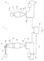
- the lithographic projection apparatus as depicted in fig. 1 comprises an exposure system 2 and a measurement system 3.
- the exposure system 2 comprises a radiation system 4, such as a light source for generating a projection beam of radion 5 and a prism (or other deflection means) 4a, a support structure for the patterning means 6a, such as a reticle, a substrate table 7 for holding a first substrate 8, and a projection system 9 for projecting the patterned beam onto a target portion of the second substrate 13.
- a radiation system 4 such as a light source for generating a projection beam of radion 5 and a prism (or other deflection means) 4a
- a support structure for the patterning means 6a such as a reticle
- a substrate table 7 for holding a first substrate 8
- a projection system 9 for projecting the patterned beam onto a target portion of the second substrate 13.
- the optical measurement device can for example comprise a radiation system 11a, a projection system 11b and further elements (not shown) for measuring a surface property of the target portion of the second substrate 13 by means of reflection, a geometric change, absorption, diffraction or any other physical phenomena due to the projection of the measurement beam 12 on the target portion of the second substrate 13.
- the measurement system 2 further comprises a second substrate table 14 for holding the second substrate 13 and second control means 15 for moving at least a part of the measurement system 2, such that the measurement beam is movable over the substrate 13.
- the exposure system 2 exposes target portions of the first substrate and thus projects the pattern provided by the patterning means 6c onto the first substrate 8.
- the substrate table 7 is moved under control of the first control means 10, such that the patterned beam moves with respect to the first substrate 8, thus providing the possibility for scanning the first substrate and exposing each desired part of the first substrate.
- the measurement system 3 measures a surface property, such as a flatness of a second substrate 13.
- a scanning movement of the measurement beam 12 with respect to the second substrate 13 is accomplished, as explained above by moving the second substrate 13 and the correction beam 12 with respect to each other.
- exposing a first substrate 8 and measuring a second substrate 13 can be performed simultaneously.
- Each of the movable parts, in this example the substrate table 7 and the substrate table 14, is controlled by respective control means 10, 15 controlling a position of the respective substrate table 7, 14.
- the control means 10, 15 each form a close loop control circuit with respective position detection means 7a, 14a, such as position sensors, acceleration sensors, etc.
- the structure of the first and second control means will be explained in more detail below.
- the system further comprises correction determination means 16 for determining a correction signal. The correction signal is fed via feeding means 17 into the first control means 10.
- the correction determination means 16 are supplied with position information regarding a position of the first and second substrate table, the position information being supplied by the respective position sensors 7a and 14a of the first and second substrate tables 7 and 14.
- the calculation determination means calculate a correction signal from the information provided by the sensors 7a and 14a.
- the correction signal provides a correction for a disturbance and consequently a position error in the exposure system which is caused by a movement of the movable part (in this example the movable substrate table 14) of the measurement system 3. Due to the movement of the movable parts, pressure waves in air surrounding the respective movable parts are generated, which pressure waves tend to cause disturbances in the other system (in this example the exposure system 2).
- the correction determination means 16 in this embodiment calculate the correction signal from an acceleration of the movable part of the measurement system (i.e. the second table 14) and a distance between the respective movable parts, i.e. in this example the first and second substrate tables 7 and 14.
- the sensor 14a comprises an acceleration sensor for measuring an acceleration of the substrate table 14 as well as position sensors for detecting a position of the second substrate table 14.
- the sensor 7a in this example comprises at least a position sensor for detecting the position of the first substrate table 7.
- the position of both substrate tables 7 and 14 as well as the acceleration of the second substrate table 14 is provided to the correction determination means. From the positions of the first and second substrate tables 7 and 14 a distance between these substrate tables is calculated by the correction determination means 16, the distance being applied for calculating the correction signal.
- F is the correction signal
- C constant
- Acc the acceleration
- D the distance between the movable parts of the exposure system and de measurement system.
- a position of a movable part of the exposure system is corrected, thus Acc being the acceleration of the other movable part, thus the movable part of the measurement system.
- Fig. 2a and fig. 2b highly schematically show a top view of a movable part 100 of a measurement system and a movable part 101 of an exposure system.
- Fig. 2a as well as fig. 2b also show a coordinate system comprising an x axis and an y axis.
- the x axis and y axis are defined in a plane in which the movable parts 100 and 101 are movable.
- a correction signal is calculated by the correction determination means which at least partly counteract an influence of the disturbance 101a.
- F x, y C * Acc x,y D 2 xy
- F x,y is the correction signal in x and y direction respectively
- C is a constant
- Acc x,y is the acceleration in x and y direction respectively
- D xy is the distance between the movable parts of the exposure system and the measurement system.
- the displacement of the movable part 100 which is schematically indicated by the 100a causes a pressure wave in the surrounding air which influences the movable part 101 and causes a disturbance indicated by the arrows 101a and 101b.
- the disturbance indicated by the arrow 101a is in the direction of the y axis
- the disturbance indicated by the arrow 101b is in the direction of the x axis.
- the displacement 100a which is in the direction of the y axis causes a disturbance of the movable part 101 in the direction of the x axis as well as the direction of the y axis.
- the correction determination means are adapted for calculating the correction signal comprising a component for at least partly compensating the disturbance 101a in the y direction and a component for at least partly compensating the disturbance 101b in the x direction.
- F x to y, y to x is the x to y and the y to x correction signal respectively
- C is a constant
- Acc x,y is the acceleration in x and y direction respectively
- D x is the distance between the movable parts of the exposure system and the measurement system in x direction
- D y is the distance between the movable parts of the exposure system and the measurement system in y direction.
- F x to y represents a correction in the y direction due to a movement of the other movable part in the x direction and vice versa.
- the distances D x and D y are indicated in fig. 2b..
- a calculation of the x to y and y to x compensation will result in a correction having a value zero, while the larger the distance D x (fig, 2b as compared to fig. 2a), the larger the x to y- and/or y to x-compensation signal will be.
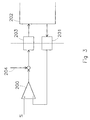
- Fig. 3 shows a more detailed schematic representation of a closed loop control loop comprising the first control means 10 as depicted in fig. 1.
- the first control means comprise a regulator 200 having two inputs.
- a first input of the regulator 200 is connected to a set point signal S which provides a set point, i.e. a signal representing a desired position of the movable part.
- the other input of the regulator 200 is connected to a sensor, 201, such as a position sensor or an acceleration sensor which detects a position or acceleration of the movable part 202.
- the movable part of which only a highly schematically depicted part is shown, is positioned by positioning means 203, such as an actuator.
- the positioning means 203 are driven by an output signal of the regulator 200.
- the regulator 200 can for example be an analogue electronic regulator, however it is also possible that the regulator 200 is implemented by means of suitable software instructions running on a microprocessor or a microcomputer.
- the regulator 200 can comprise integration, proportional regulation, differentiation or any suitable operations.
- the dotted line which crosses the positioning means 203 and the sensor 201 represents a separation between an "electronic" or “control” part and a "physical” part. The increase of a disturbance due to displacement of another movable part of the projection apparatus, air pressure fluctuations or pressure waves caused by this displacement will result in a disturbance of the movable part 202.
- a compensation signal 204 is added to the output signal of the regulator 200, thus feeding the correction signal into the control loop.
- the control means comprise a digital regulator, comprising dedicated hardware or programmed in software
- the feeding means for feeding the correction signal into the control means for example comprise a digital addition of subtraction implemented in either hardware or software, however it is also possible that the feeding means comprise any other suitable means for feeding the correction signal into the respective control means, such as an analogue addition adding a voltage or a current, any suitable means, or any other way of feeding the correction signal into the control means.
- the feeding means according to this embodiment comprise a delay for delaying the correction signal. The delay in this example matches a delay of the digital control means, such that adverse effects due to for example a to early compensation by the correction signal are largely eliminated; thus the feeding means add the correction signal to a control signal at the output of the regulator in the closed loop control.
- Fig. 4 shows the device manufacturing method according to the invention.
- a first substrate is provided.
- the first substrate is at least partly covered by a layer of radiation-sensitive material.
- a projection beam is provided using a radiation system.
- pattern means are used to endow the projection beam with a pattern in its cross-section.
- the patterned beam is projected onto a target potion of the layer of radiation-sensitive material on the first substrate.
- the patterned beam is moved with respect to the first substrate.
- a second substrate is provided while in step 306 a measurement beam is projected on a target portion of the second substrate and a surface property of the target portion of de second substrate is measured.
- the measurement beam is moved over a relevant portion of the surface of the second substrate.
- the respective beam can move with respect to, such as scan, a relevant portion of the respective substrate.
- the patterned beam scans a relevant portion of the first substrate while the measurement beam scans a relevant portion of the second substrate.
- a correction signal is determined for at least partly correcting an error of a position of the patterned beam on the first substrate, the error by a movement of a device for moving the measurement beam with respect to the second substrate.
- step 308 comprises the step of determining a correction signal for at least partly correcting an error of a position of the measurement beam on the second substrate, the error by a movement of a device for moving the patterned beam with respect to the first substrate.
- step 309 the position of the patterned beam with respect to the first substrate is corrected with the correction signal.
- step 308 the position of the measurement beam with respect to the second substrate is corrected with the correction signal.
- a compensation for compensating an error caused by a displacement of air due to a movement of a movable part of a lithographic system, the error being caused by displacement of air or pressure waves in the air due to a movement of another movable part of the lithographic apparatus.
- the compensation is calculated based on the acceleration of the movable part which causes the disturbance, and the distance (more preferably the inverse of the square distance) between the respective movable parts.
- An embodiment of the invention can also be worded as a lithographic projection apparatus comprising an exposure system and a measurement system, the exposure system comprising:
- the method according to the invention can also be worded as a device manufacturing method comprising the steps of:
Landscapes
- Physics & Mathematics (AREA)
- General Physics & Mathematics (AREA)
- Exposure And Positioning Against Photoresist Photosensitive Materials (AREA)
Priority Applications (1)
| Application Number | Priority Date | Filing Date | Title |
|---|---|---|---|
| EP04076864A EP1494078A1 (de) | 2003-07-01 | 2004-06-28 | Lithographischer Apparat und Verfahren zur Herstellung einer Vorrichtung |
Applications Claiming Priority (3)
| Application Number | Priority Date | Filing Date | Title |
|---|---|---|---|
| EP03077048 | 2003-07-01 | ||
| EP03077048 | 2003-07-01 | ||
| EP04076864A EP1494078A1 (de) | 2003-07-01 | 2004-06-28 | Lithographischer Apparat und Verfahren zur Herstellung einer Vorrichtung |
Publications (1)
| Publication Number | Publication Date |
|---|---|
| EP1494078A1 true EP1494078A1 (de) | 2005-01-05 |
Family
ID=33436120
Family Applications (1)
| Application Number | Title | Priority Date | Filing Date |
|---|---|---|---|
| EP04076864A Withdrawn EP1494078A1 (de) | 2003-07-01 | 2004-06-28 | Lithographischer Apparat und Verfahren zur Herstellung einer Vorrichtung |
Country Status (1)
| Country | Link |
|---|---|
| EP (1) | EP1494078A1 (de) |
Cited By (2)
| Publication number | Priority date | Publication date | Assignee | Title |
|---|---|---|---|---|
| CN101441419B (zh) * | 2007-10-10 | 2011-03-16 | Asml荷兰有限公司 | 衬底传送方法、传送系统和光刻投影设备 |
| CN103365118A (zh) * | 2013-07-19 | 2013-10-23 | 中国科学院上海光学精密机械研究所 | 光刻机光束监测系统的标定装置及标定方法 |
Citations (5)
| Publication number | Priority date | Publication date | Assignee | Title |
|---|---|---|---|---|
| EP0557100A1 (de) * | 1992-02-21 | 1993-08-25 | Canon Kabushiki Kaisha | System zum Steuern von Trägerplatten |
| US20010015799A1 (en) * | 2000-01-11 | 2001-08-23 | Toshiya Asano | Stage apparatus, exposure apparatus, and device production method |
| US20020001915A1 (en) * | 2000-07-03 | 2002-01-03 | Satoshi Akimoto | Step & scan projection exposure apparatus, maintenance method therefor, and semiconductor device manufacturing method and semiconductor manufacturing factory using the apparatus |
| EP1186959A2 (de) * | 2000-09-07 | 2002-03-13 | Asm Lithography B.V. | Verfahren zur Eichung eines lithographischen Projektionsapparats |
| EP1347498A2 (de) * | 2002-02-26 | 2003-09-24 | Canon Kabushiki Kaisha | Vorrichtung zur Ausrichtung eines Trägers und Kontrollverfahren dafür |
-
2004
- 2004-06-28 EP EP04076864A patent/EP1494078A1/de not_active Withdrawn
Patent Citations (5)
| Publication number | Priority date | Publication date | Assignee | Title |
|---|---|---|---|---|
| EP0557100A1 (de) * | 1992-02-21 | 1993-08-25 | Canon Kabushiki Kaisha | System zum Steuern von Trägerplatten |
| US20010015799A1 (en) * | 2000-01-11 | 2001-08-23 | Toshiya Asano | Stage apparatus, exposure apparatus, and device production method |
| US20020001915A1 (en) * | 2000-07-03 | 2002-01-03 | Satoshi Akimoto | Step & scan projection exposure apparatus, maintenance method therefor, and semiconductor device manufacturing method and semiconductor manufacturing factory using the apparatus |
| EP1186959A2 (de) * | 2000-09-07 | 2002-03-13 | Asm Lithography B.V. | Verfahren zur Eichung eines lithographischen Projektionsapparats |
| EP1347498A2 (de) * | 2002-02-26 | 2003-09-24 | Canon Kabushiki Kaisha | Vorrichtung zur Ausrichtung eines Trägers und Kontrollverfahren dafür |
Cited By (3)
| Publication number | Priority date | Publication date | Assignee | Title |
|---|---|---|---|---|
| CN101441419B (zh) * | 2007-10-10 | 2011-03-16 | Asml荷兰有限公司 | 衬底传送方法、传送系统和光刻投影设备 |
| CN103365118A (zh) * | 2013-07-19 | 2013-10-23 | 中国科学院上海光学精密机械研究所 | 光刻机光束监测系统的标定装置及标定方法 |
| CN103365118B (zh) * | 2013-07-19 | 2015-03-25 | 中国科学院上海光学精密机械研究所 | 光刻机光束监测系统的标定装置及标定方法 |
Similar Documents
| Publication | Publication Date | Title |
|---|---|---|
| US6765218B2 (en) | Lithographic projection apparatus with positioning system for use with reflectors | |
| US5593800A (en) | Mask manufacturing method and apparatus and device manufacturing method using a mask manufactured by the method or apparatus | |
| US7126671B2 (en) | Lithographic apparatus and device manufacturing method | |
| EP1345082A1 (de) | Lithographischer Apparat und Verfahren zur Herstellung einer Vorrichtung | |
| EP1465018B1 (de) | Korrektur in Abtastrichtung der Verschiebung zwischen Maske und Objekt infolge einer Z-Verschiebung und einer nicht-senkrechten Beleuchtung | |
| CN101641645B (zh) | 器件制造方法、光刻设备 | |
| CN100507718C (zh) | 投影系统及利用该投影系统的方法 | |
| US7633600B2 (en) | Lithographic apparatus and device manufacturing method | |
| US7804584B2 (en) | Integrated circuit manufacturing methods with patterning device position determination | |
| EP1107068B1 (de) | Lithographischer Projektionsapparat mit System zur Positionierung eines Reflektors | |
| EP1469348B1 (de) | Projektionssystem und Verfahren zu dessen Verwendung | |
| US7148950B2 (en) | Lithographic apparatus and device manufacturing method | |
| KR100585465B1 (ko) | 리소그래피 투영장치, 디바이스제조방법, 이것에 의하여제조된 디바이스 및 측정방법 | |
| US7379156B2 (en) | Lithographic apparatus and device manufacturing method | |
| EP1494078A1 (de) | Lithographischer Apparat und Verfahren zur Herstellung einer Vorrichtung | |
| US7177059B2 (en) | Device and method for manipulation and routing of a metrology beam | |
| US6992752B2 (en) | Lithographic projection apparatus, computer program for control thereof, and device manufacturing method | |
| EP1465015A1 (de) | Lithographischer Apparat und Verfahren zur Herstellung einer Vorrichtung | |
| EP1146395A2 (de) | Lithographischer Apparat, Verfahren zur Herstellung einer Vorrichtung, sowie durch dieses Verfahren hergestellte Vorrichtung | |
| EP1267213B1 (de) | Lithographischer Projektionsapparat | |
| EP1335248A1 (de) | Lithographischer Apparat und Verfahren zur Herstellung einer Vorrichtung | |
| EP1345084A1 (de) | Lithographischer Apparat und Verfahren zur Herstellung einer Vorrichtung |
Legal Events
| Date | Code | Title | Description |
|---|---|---|---|
| PUAI | Public reference made under article 153(3) epc to a published international application that has entered the european phase |
Free format text: ORIGINAL CODE: 0009012 |
|
| AK | Designated contracting states |
Kind code of ref document: A1 Designated state(s): AT BE BG CH CY CZ DE DK EE ES FI FR GB GR HU IE IT LI LU MC NL PL PT RO SE SI SK TR |
|
| AX | Request for extension of the european patent |
Extension state: AL HR LT LV MK |
|
| 17P | Request for examination filed |
Effective date: 20050628 |
|
| AKX | Designation fees paid |
Designated state(s): DE FR GB IT NL |
|
| GRAP | Despatch of communication of intention to grant a patent |
Free format text: ORIGINAL CODE: EPIDOSNIGR1 |
|
| INTG | Intention to grant announced |
Effective date: 20130709 |
|
| STAA | Information on the status of an ep patent application or granted ep patent |
Free format text: STATUS: THE APPLICATION IS DEEMED TO BE WITHDRAWN |
|
| 18D | Application deemed to be withdrawn |
Effective date: 20131120 |