EP1494200A2 - Anzeigegerät - Google Patents
Anzeigegerät Download PDFInfo
- Publication number
- EP1494200A2 EP1494200A2 EP04015138A EP04015138A EP1494200A2 EP 1494200 A2 EP1494200 A2 EP 1494200A2 EP 04015138 A EP04015138 A EP 04015138A EP 04015138 A EP04015138 A EP 04015138A EP 1494200 A2 EP1494200 A2 EP 1494200A2
- Authority
- EP
- European Patent Office
- Prior art keywords
- display
- signal
- emission
- correction
- display device
- Prior art date
- Legal status (The legal status is an assumption and is not a legal conclusion. Google has not performed a legal analysis and makes no representation as to the accuracy of the status listed.)
- Withdrawn
Links
- 239000003086 colorant Substances 0.000 claims abstract description 28
- 239000011159 matrix material Substances 0.000 claims abstract description 5
- 238000000034 method Methods 0.000 claims description 6
- 239000000463 material Substances 0.000 description 9
- 230000007423 decrease Effects 0.000 description 8
- 238000001514 detection method Methods 0.000 description 6
- 238000010586 diagram Methods 0.000 description 5
- 230000006870 function Effects 0.000 description 4
- 230000001276 controlling effect Effects 0.000 description 3
- 230000002093 peripheral effect Effects 0.000 description 3
- 230000003247 decreasing effect Effects 0.000 description 2
- 230000001105 regulatory effect Effects 0.000 description 2
- CIWBSHSKHKDKBQ-JLAZNSOCSA-N Ascorbic acid Chemical compound OC[C@H](O)[C@H]1OC(=O)C(O)=C1O CIWBSHSKHKDKBQ-JLAZNSOCSA-N 0.000 description 1
- 108010043121 Green Fluorescent Proteins Proteins 0.000 description 1
- 230000000694 effects Effects 0.000 description 1
- 238000005401 electroluminescence Methods 0.000 description 1
- 239000002245 particle Substances 0.000 description 1
- 230000004044 response Effects 0.000 description 1
- 238000005070 sampling Methods 0.000 description 1
- 238000005303 weighing Methods 0.000 description 1
Images


Classifications
-
- G—PHYSICS
- G09—EDUCATION; CRYPTOGRAPHY; DISPLAY; ADVERTISING; SEALS
- G09G—ARRANGEMENTS OR CIRCUITS FOR CONTROL OF INDICATING DEVICES USING STATIC MEANS TO PRESENT VARIABLE INFORMATION
- G09G3/00—Control arrangements or circuits, of interest only in connection with visual indicators other than cathode-ray tubes
- G09G3/20—Control arrangements or circuits, of interest only in connection with visual indicators other than cathode-ray tubes for presentation of an assembly of a number of characters, e.g. a page, by composing the assembly by combination of individual elements arranged in a matrix no fixed position being assigned to or needed to be assigned to the individual characters or partial characters
- G09G3/2003—Display of colours
-
- G—PHYSICS
- G09—EDUCATION; CRYPTOGRAPHY; DISPLAY; ADVERTISING; SEALS
- G09G—ARRANGEMENTS OR CIRCUITS FOR CONTROL OF INDICATING DEVICES USING STATIC MEANS TO PRESENT VARIABLE INFORMATION
- G09G2320/00—Control of display operating conditions
- G09G2320/02—Improving the quality of display appearance
- G09G2320/0271—Adjustment of the gradation levels within the range of the gradation scale, e.g. by redistribution or clipping
-
- G—PHYSICS
- G09—EDUCATION; CRYPTOGRAPHY; DISPLAY; ADVERTISING; SEALS
- G09G—ARRANGEMENTS OR CIRCUITS FOR CONTROL OF INDICATING DEVICES USING STATIC MEANS TO PRESENT VARIABLE INFORMATION
- G09G2320/00—Control of display operating conditions
- G09G2320/06—Adjustment of display parameters
- G09G2320/0666—Adjustment of display parameters for control of colour parameters, e.g. colour temperature
-
- G—PHYSICS
- G09—EDUCATION; CRYPTOGRAPHY; DISPLAY; ADVERTISING; SEALS
- G09G—ARRANGEMENTS OR CIRCUITS FOR CONTROL OF INDICATING DEVICES USING STATIC MEANS TO PRESENT VARIABLE INFORMATION
- G09G2320/00—Control of display operating conditions
- G09G2320/06—Adjustment of display parameters
- G09G2320/0673—Adjustment of display parameters for control of gamma adjustment, e.g. selecting another gamma curve
-
- G—PHYSICS
- G09—EDUCATION; CRYPTOGRAPHY; DISPLAY; ADVERTISING; SEALS
- G09G—ARRANGEMENTS OR CIRCUITS FOR CONTROL OF INDICATING DEVICES USING STATIC MEANS TO PRESENT VARIABLE INFORMATION
- G09G2360/00—Aspects of the architecture of display systems
- G09G2360/16—Calculation or use of calculated indices related to luminance levels in display data
-
- G—PHYSICS
- G09—EDUCATION; CRYPTOGRAPHY; DISPLAY; ADVERTISING; SEALS
- G09G—ARRANGEMENTS OR CIRCUITS FOR CONTROL OF INDICATING DEVICES USING STATIC MEANS TO PRESENT VARIABLE INFORMATION
- G09G3/00—Control arrangements or circuits, of interest only in connection with visual indicators other than cathode-ray tubes
- G09G3/20—Control arrangements or circuits, of interest only in connection with visual indicators other than cathode-ray tubes for presentation of an assembly of a number of characters, e.g. a page, by composing the assembly by combination of individual elements arranged in a matrix no fixed position being assigned to or needed to be assigned to the individual characters or partial characters
- G09G3/22—Control arrangements or circuits, of interest only in connection with visual indicators other than cathode-ray tubes for presentation of an assembly of a number of characters, e.g. a page, by composing the assembly by combination of individual elements arranged in a matrix no fixed position being assigned to or needed to be assigned to the individual characters or partial characters using controlled light sources
- G09G3/28—Control arrangements or circuits, of interest only in connection with visual indicators other than cathode-ray tubes for presentation of an assembly of a number of characters, e.g. a page, by composing the assembly by combination of individual elements arranged in a matrix no fixed position being assigned to or needed to be assigned to the individual characters or partial characters using controlled light sources using luminous gas-discharge panels, e.g. plasma panels
- G09G3/288—Control arrangements or circuits, of interest only in connection with visual indicators other than cathode-ray tubes for presentation of an assembly of a number of characters, e.g. a page, by composing the assembly by combination of individual elements arranged in a matrix no fixed position being assigned to or needed to be assigned to the individual characters or partial characters using controlled light sources using luminous gas-discharge panels, e.g. plasma panels using AC panels
- G09G3/291—Control arrangements or circuits, of interest only in connection with visual indicators other than cathode-ray tubes for presentation of an assembly of a number of characters, e.g. a page, by composing the assembly by combination of individual elements arranged in a matrix no fixed position being assigned to or needed to be assigned to the individual characters or partial characters using controlled light sources using luminous gas-discharge panels, e.g. plasma panels using AC panels controlling the gas discharge to control a cell condition, e.g. by means of specific pulse shapes
- G09G3/294—Control arrangements or circuits, of interest only in connection with visual indicators other than cathode-ray tubes for presentation of an assembly of a number of characters, e.g. a page, by composing the assembly by combination of individual elements arranged in a matrix no fixed position being assigned to or needed to be assigned to the individual characters or partial characters using controlled light sources using luminous gas-discharge panels, e.g. plasma panels using AC panels controlling the gas discharge to control a cell condition, e.g. by means of specific pulse shapes for lighting or sustain discharge
Definitions
- the present invention relates to a display device using a self emitting flat display panel, such as a plasma display panel (hereafter called “PDP”) and an electroluminescence (hereafter called “EL”) panel.
- a self emitting flat display panel such as a plasma display panel (hereafter called “PDP”) and an electroluminescence (hereafter called “EL”) panel.
- PDP plasma display panel
- EL electroluminescence
- ABL Automatic Brightness Limiting
- total number of SUS the total number of sustain pulses to be applied to the PDP during one field period, that is the total number of sustain pulses to be applied to the subfields of one field period (hereafter called "total number of SUS"), is gradually decreased as the APL increases.
- the total number of SUS is maintained to be a predetermined constant value.
- the total number of SUS is decreased as the APL increases, so as to decrease power consumption.
- the number of times of light emission from fluorescent elements, included in the display cells arrayed on the PDP also decreases.
- Red, green and blue colors are hereafter called R, G and B respectively.
- One pixel on the display screen is defined by a combination of display cells (combination of these three different fluorescent materials). Display cells emit different colors according to the signal levels of the pixel signals of the respective colors included in the image signal, and a color screen is displayed on the display panel.
- the afterglow characteristics of these fluorescent materials are different, depending on the colors of the fluorescent materials.
- the brightness ratio of each of the R, G and B fluorescent materials at emission is not constant if the number of times of emission changes. Therefore, even if the white balance is corrected at a predetermined number of times of emission on the basis of the brightness of each fluorescent material (i.e., the emission brightness of the display cell for each color is corrected) so that all the R, G and B display cells emit in combination white light, the white balance is lost if the number of times of emission of the fluorescent materials changes.
- the afterglow characteristics of the G fluorescent material normally have a bigger value than those of the other fluorescent materials. Therefore as the APL increases and the total number of SUS decreases, that is, as the pulse density per unit time of sustain pulses decreases, the emission brightness of the G component relatively increases and makes the display screen of the PDP greenish. So if the white balance correction is set in advance based on the pulse density at an intermediate value of the APL, then the entire screen becomes greenish even if the APL increases and the pulse density decreases to attempt to create an entirely white screen. If the APL decreases and the pulse density increases to reduce the white area on the screen, on the other hand, the entire screen becomes reddish.
- the drive current of the sustain pulse drive circuit also changes.
- Such a change of the drive current causes a distortion of pulse waveforms to be supplied to the PDP by the influence of switching resistance and the drive impedance of the sustain pulse drive circuit.
- the emission brightness of the display cells changes. This further increases the loss of white balance, in addition to the difference caused by the above mentioned afterglow characteristics for each fluorescent material.
- One object of the present invention is to provide a display device which can maintain the white balance even if the brightness of the display image changes.
- an improved display device for displaying an image on a display panel in accordance with an input image signal.
- the display panel includes a plurality of display cells, and these display cells are divided into a plurality of groups. Each display cell group serves as a pixel.
- the display cell groups are arranged in a matrix.
- the display cells in each group have different emission colors. Emission of respective colors are determined by signal levels of pixel signals included in the input image signal.
- the display device includes a brightness level calculation unit for calculating emission brightness of the image and generating a brightness level signal that represents a level of the emission brightness.
- the display device also includes an emission level correction unit for correcting the signal levels of the pixel signals included in the image signal for the respective emission colors based on the brightness level signal.
- an improved drive method for a display device is adapted to display an image on a display panel in accordance with an input image signal.
- the display panel includes a plurality of display cells, and these display cells are divided into a plurality of groups. Each display cell group serves as a pixel.
- the display cell groups are arranged in a matrix.
- the display cells in each group have different emission colors, and emission of respective colors are determined by signal levels of pixel signals included in the input image signal.
- a display period of each field of the input image signal is divided into of a plurality of subfields.
- a predetermined number of sustain pulses is set for each subfield.
- Each of the display cells is set into a lit mode or an unlit mode in each subfield in accordance with the input image signal.
- the signal levels of the pixel signals included in the image signal are corrected for the respective emission colors based on a total number of sustain pulses repeatedly applied in the subfield or a period of the sustain pulses.
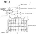
- the display device 10 according to the first embodiment of the present invention is shown in Fig. 1, and includes an analog-to-digital converter 11 (hereafter called "AD converter 11"), a synchronization detection section 12, a display data generation section 20, an image memory section 30, a driver control section 40, a PDP 50, an address driver circuit 60, an X sustain driver circuit 70 and a Y sustain driver circuit 80.
- the display data generation section 20 mainly corresponds to the brightness level calculation means and emission level correction means set forth in the appended claims.
- the AD converter 11 is a circuit for converting the image signals supplied from an image source (not illustrated), such as a digital broadcast receiver or video disk player, into digital pixel signals having a predetermined bit length at a predetermined sampling rate.
- the synchronization detection section 12 is a circuit for detecting the horizontal and vertical synchronization signals included in the image signals, and notifying such synchronization timing to the display data generation section 20 and the driver control section 40.
- the display data generation section 20 is a circuit for generating the display pixel signals to be displayed on the display screen by performing a predetermined processing on the digital pixel signals supplied from the AD converter 11.
- Fig. 2 shows the configuration of the display data generation section 20.
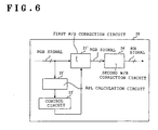
- the display data generation section 20 includes a first white balance correction circuit 21 (hereafter called “first correction circuit 21"), APL calculation circuit 22, control circuit 23, and second white balance correction circuit 24 (hereafter called “second correction circuit 24").
- the APL calculation circuit 22 and control circuit 23 mainly correspond to the brightness level calculation means in the appended claims
- the first correction circuit 21, second correction circuit 24 and control circuit 23 mainly correspond to the emission level correction means in the appended claims.
- the first correction circuit 21 corresponds to the first correction means
- the second correction circuit 24 corresponds to the second correction means.
- the first correction circuit 21 is a circuit for correcting the white balance of the display screen by correcting the signal levels of the digital pixel signals for respective emission colors using the correction values stored in the correction value table.
- the correction value table is prepared in advance.
- the APL calculation circuit 22 is a circuit for calculating the emission brightness of the display image, generating the brightness level signal which indicates the brightness level, and supplying the brightness level signal to the control circuit 23.
- the control circuit 23 includes a microcomputer, a memory circuit having a RAM and a ROM, and peripheral circuits thereof (none of these are illustrated) for controlling the entire display data generation section 20.
- the second correction circuit 24 is a circuit for adjusting the white balance of the display screen by performing predetermined arithmetic processing on the signal levels of the digital pixel signals, and correcting the signal levels for respective emission colors.
- the display data generation section 20 includes a multi-grayscale processing circuit and various circuits required for creating display image data, such as a dither processing circuit, but the block diagram in Fig. 2 shows only the elements related to the embodiment of the present invention.
- the image memory section 30 is an image memory circuit for temporarily storing display pixel signals supplied from the display data generation section 20 for one field to several fields, for example.
- the display pixel signals stored in the image memory section 30 are supplied to the address driver 60 based on timing signals supplied from the driver control section 40.
- the driver control section 40 generates control signals for driving the address driver and the X and Y sustain drivers based on the synchronization timing signals included in the image signals, and supplies the control signals to the respective drivers.
- the PDP 50 is a display screen for displaying images, and includes row electrodes X 1 to X n and row electrodes Y 1 to Y n . Each pair of row electrodes X i and Y i defines each display line (first row to n-th row) of one screen.
- column electrodes Z 1 to Z m are also provided corresponding to vertical lines (first column to m-th column) of one screen. The column electrodes extend perpendicularly to the row electrode pairs. The dielectric layer and the discharge space layer, which are not illustrated, are sandwiched between the column electrodes and the row electrode pairs.
- One display cell C (i, j) is formed at a cross-section of a pair of row electrodes (X i , Y i ) and one column electrode Z j .
- the electrodes of the PDP 50 are connected to the address driver 60, X sustain driver 70 and Y sustain driver 80, and these driver circuits are controlled by instructions from the driver control section 40.
- the Y sustain driver 80 generates various drive pulses including the reset pulse and sustain pulse, and applies these pulses to the row electrodes Y 1 to Y n at a predetermined timing.
- the X sustain driver 70 also generates various drive pulses and applies these pulses to the row electrodes X 1 to X n at a predetermined timing.
- the address driver 60 generates the pixel signal pulses corresponding to the first to n-th rows of the display screen from the display pixel signals supplied from the image memory section 30 based on the timing signals from the driver control section 40, and sequentially applies these pulses to the column electrodes Z 1 to Z n .
- a pulse generation circuit (not illustrated) for generating various drive pulses is disposed for each row and column electrode of the PDP 50.
- the Y sustain driver 80 generates reset pulses PR y with a positive voltage as shown in the timing chart in Fig. 3, and applies these pulses to the row electrodes Y 1 to Y n simultaneously.
- the X sustain driver 70 generates reset pulses RP x with a negative voltage, and applies these pulses to all the row electrodes X 1 to X n simultaneously.
- reset pulses RP x and RP y By applying these reset pulses RP x and RP y simultaneously, all the display cells of the PDP 50 are discharged and excited, and charged particles are generated. After the discharge ends, a certain amount of wall charges are formed uniformly in the dielectric layers of all the display cells. This processing is called the "reset step".
- the address driver 60 After the reset step ends, the address driver 60 generates pixel signal pulses DP 1 to DP n according to the pixel signals of the first row to n-th row of the screen. The address driver 60 sequentially applies these pixel signal pulses to the column electrodes Z 1 to Z m , as shown in Fig. 3.
- the Y sustain driver 80 on the other hand, generates scan pulses SP with a negative voltage according to the respective application timing of the pixel signal pulses DP 1 to DP n .
- the Y sustain driver 80 sequentially applies these scan pulses SP to the row electrodes Y 1 to Y n at the timing shown in Fig. 2.
- the Y sustain driver 80 continuously applies the sustain pulses IP y with a positive voltage to the row electrodes Y 1 - Y n , as shown in Fig. 3.
- the X sustain driver 70 continuously applies the sustain pulses IP x with a positive voltage to the row electrodes X 1 to X n at a timing shifted from the application timing of the sustain pulses IP y .
- discharge emission is repeated in the emission discharge cells where the wall charges remain, and the emission status of these display cells is maintained. This processing step is called the "sustain step".
- FIG. 4 An overview of the program for such processing is shown in the flow chart in Fig. 4.
- This program has been stored in the ROM of the control circuit 23 in advance, and the microcomputer in the control circuit 23 executes this program one step at a time, synchronizing with the internal clock signals.
- the program shown in Fig. 4 may be started up for each screen synchronizing with the detection timing of the vertical synchronization signals from the synchronization detection section 12, or may be started up according to a predetermined timing.
- the microcomputer of the control circuit 23 sends instructions to the APL calculation circuit 22, and has this circuit calculate the APL of the image data which is output from the first correction circuit 21 in step S11.
- the first white balance correction has been performed by the correction value table included in the first correction circuit.
- the white balance correction by the correction value table is executed according to the following procedure. At first, the correction values which have been stored in the addresses corresponding to R, G and B pixel signal values to be supplied to the first correction circuit 21 are extracted from the correction value table in which the correction values are set in advance based on the emission characteristics of the display panel. Then correction is made by performing a weighing on the signal level of the pixel signal for each color using the extracted correction values.
- the microcomputer Upon receiving the APL of the image data from the APL calculation circuit 22, the microcomputer moves to the next step S12, and decides the total number of SUS corresponding to the acquired APL and the pulse density of the sustain pulses in the sustain step.
- the microcomputer moves to the next step S13 and decides correction values for the second correction circuit 24. Specifically, based on the total number of SUS and the pulse density determined in step S12, the microcomputer calculates the gain value to multiply and the offset value to be superimposed for each of the R, G and B pixel signals. It should be noted that the gain value and offset value may be obtained using a prepared numerical table on the basis of the total number of SUS and pulse density. Alternatively, a predetermined function may be established in advance between the total number of SUS, pulse density, gain value and offset value, so as to use this function for calculation of the gain value and offset value.
- step S13 Upon finishing each correction value decision processing in step S13, the microcomputer moves to the next step S14, and transfers the calculated correction values to the second correction circuit 24.
- Fig. 5 shows the principle of the white balance correction in the second correction circuit 24.
- the signal level of the output pixel signal may be adjusted by multiplying the input pixel signal by the gain value transferred from the control circuit 23.
- the signal level of the output pixel signal may be adjusted by superimposing the transferred offset value onto the input pixel signal.
- Such correction processing is executed for each of the R, G and B pixels.
- the processing described above is executed for each display screen. Therefore, even if the brightness of the display screen changes, appropriate white balance correction is executed according to the most recent brightness.
- the display data generation section 20 in the second embodiment includes a first white balance correction circuit 21' (hereafter called “first correction circuit 21'"), APL calculation circuit 22' , control circuit 23' and second white balance correction circuit 24' (hereafter called “second correction circuit 24'").
- the APL calculation circuit 22' and control circuit 23' mainly correspond to the brightness level calculation means in the appended claims
- the first correction circuit 21' , second correction circuit 24' and control circuit 23' mainly correspond to the emission level correction means in the appended claims.
- the first correction circuit 21' corresponds to the first correction means
- the second correction circuit 24' corresponds to the second correction means respectively.
- the first correction circuit 21' is a circuit for correcting the white balance of the display screen by adjusting the signal level of the digital pixel signal for each emission color using the correction values stored in the correction value table.
- the APL calculation circuit 22' is a circuit for calculating the emission brightness of the display image, generating the brightness level signal which indicates the brightness level, and supplying the brightness level signal to the control circuit 23'.
- the control circuit 23' includes a microcomputer, a memory circuit having a RAM and a ROM, and peripheral circuits thereof (none of these are illustrated), and operates and controls the entire display data generation section 20.
- the second correction circuit 24' is a circuit for correcting the white balance of the display screen by performing predetermined arithmetic processing on the signal levels of the digital pixel signals, and correcting the signal levels for the respective emission colors.
- description is omitted.
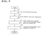
- FIG. 7 An overview of the program for such processing is shown in the flow chart in Fig. 7.
- This program has been stored in the ROM of the control circuit 23' in advance, and the microcomputer in the control circuit 23' executes this program one step at a time, synchronizing with the internal clock signals.
- the program shown in Fig. 7 may be started up for each screen synchronizing with the detection time of the vertical synchronization signals from the synchronization detection section 12, or may be started up according to a predetermined timing.
- microcomputer When the program shown in Fig. 7 is started up, the microcomputer of the control circuit 23' (hereafter simply called “microcomputer") sends predetermined instructions to the APL calculation circuit 22' , and has this circuit calculate the APL of the image data which is introduced to the first correction circuit 21' in step S21.
- microcomputer sends predetermined instructions to the APL calculation circuit 22' , and has this circuit calculate the APL of the image data which is introduced to the first correction circuit 21' in step S21.
- the microcomputer Upon receiving the APL of the image data from the APL calculation circuit 22', the microcomputer moves to the next step S22, and determines the total number of SUS corresponding to the acquired APL and the pulse density of the sustain pulses in the sustain step.
- the microcomputer moves to the next step S23, and determines the correction adjustment values for the correction values of the first correction circuit 21'. Specifically, based on the total number of SUS and pulse density decided in step S22, the microcomputer calculates the correction adjustment values for adjusting the correction values which are stored in the correction value table included in the first correction circuit 21'.
- the correction values which are set based on the emission characteristics of the display panel are stored in the correction value table.
- adjustment according to the brightness change of the display screen is further added to the correction values, so as to improve the white balance correction effect in the first correction circuit 21'.
- the correction adjustment values may be obtained from a numerical table on the basis of the total number of SUS and pulse density.
- predetermined functions are defined among the total number of SUS, pulse density and adjustment value, so as to use these functions for calculation of the adjustment values.
- the microcomputer moves to the next step S24, and transfers the calculated correction adjustment values to the first correction circuit 21'.
- the first correction circuit 21' which receives the correction adjustment values from the control circuit 23', adjusts the correction values stored in the correction value table using these correction adjustment values, and corrects the white balance for the pixel signals of the respective colors using the adjusted (modified) correction values.
- predetermined fixed values are prepared for the gain value and the offset value to be used for correction of the white balance in the second correction circuit 24'.
- the white balance correction processing in the first correction circuit 21' and the second correction circuit 24' is the same as the first embodiment, so that description thereof will be omitted.
- the processing described above is executed for each display screen. Therefore, even if the brightness of the display screen changes, appropriate white balance correction is executed according to the current screen brightness.
- the display data generation section 20 in the third embodiment includes a first white balance correction circuit 21" (hereafter called “first correction circuit 21””), APL calculation circuit 22", control circuit 23", second white balance correction circuit 24" (hereafter called “second correction circuit 24””) and a switching control circuit 25.
- the APL calculation circuit 22" and control circuit 23" mainly correspond to the brightness level calculation means in the appended claims, and the first correction circuit 21", second correction circuit 24" and control circuit 23” mainly correspond to the emission level correction means in the appended claims.
- the switching control circuit 25 corresponds to the operation switching means, the first correction circuit 21" corresponds to the first correction means, and the second correction circuit 24" corresponds to the second correction means.
- the first correction circuit 21" corrects the white balance of the display screen by correcting the signal levels of the digital pixel signals for the emission colors using the correction values stored in the correction value table.
- the APL calculation circuit 22" is a circuit for calculating the emission brightness of the display screen, generating the brightness level signal which indicates the brightness level, and supplying the brightness level signal to the control circuit 23".
- the control circuit 23" includes a microcomputer, a memory circuit having a RAM and a ROM, and peripheral circuits thereof (none of these are illustrated) for controlling the entire display data generation section 20.
- the second correction circuit 24" is a circuit for correcting the white balance of the display screen by performing arithmetic processing on the signal levels of the digital pixel signals, and correcting the signal levels for the emission colors.
- the switching control circuit 25 switches the operation of the display data generation section 20 in response to switching instructions.
- This embodiment is characterized in that operation of the display data generation section 20 is switched by the switching instructions which the user enters to the switching control circuit 25 from an operation panel (not illustrated) of the display device, for example.
- the switching control circuit 25 connects the input signal directed to the first correction circuit 21" to the APL calculation circuit 22" , and connects the output signal from the control circuit 23" to the second correction circuit 24". By these connections, the processing operation described in the first embodiment is executed.
- the switching control circuit 25 connects the output signal from the first correction circuit 21" to the APL calculation circuit 22", and connects the output signal from the control circuit 23" to the first correction circuit 21". By these connections, the processing operation described in the second embodiment is executed.
- appropriate white balance correction is performed according to the brightness change of the display screen, based on the selected processing operation.
- the present invention is not limited to the above described embodiments.
- the first correction circuit and the second correction circuit it is not necessary to always include the first correction circuit and the second correction circuit, and the display data generation section 20 may include only one of these correction circuits.
- the total number of SUS and the density of sustain pulses in one field period are determined based on the average brightness in one field period of the image signal, and the R, G and B signals are corrected (adjusted) on the basis of the total number of SUS and sustain pulse density.
- the present invention is not limited in this regard.
- the present invention can be applied as long as the R, G and B signals are respectively corrected to adjust the white balance of the display image, when the density of the sustain pulses (i.e., the period of sustain pulses which are repeatedly applied in the sustain step of each subfield) changes.
- the R, G and B signals may be respectively corrected correspondingly so as to adjust the white balance of the display image.
Landscapes
- Engineering & Computer Science (AREA)
- Physics & Mathematics (AREA)
- Computer Hardware Design (AREA)
- General Physics & Mathematics (AREA)
- Theoretical Computer Science (AREA)
- Control Of Indicators Other Than Cathode Ray Tubes (AREA)
- Control Of El Displays (AREA)
- Video Image Reproduction Devices For Color Tv Systems (AREA)
- Control Of Gas Discharge Display Tubes (AREA)
Applications Claiming Priority (2)
| Application Number | Priority Date | Filing Date | Title |
|---|---|---|---|
| JP2003192216A JP2005025058A (ja) | 2003-07-04 | 2003-07-04 | ディスプレイ装置 |
| JP2003192216 | 2003-07-04 |
Publications (2)
| Publication Number | Publication Date |
|---|---|
| EP1494200A2 true EP1494200A2 (de) | 2005-01-05 |
| EP1494200A3 EP1494200A3 (de) | 2005-08-10 |
Family
ID=33432363
Family Applications (1)
| Application Number | Title | Priority Date | Filing Date |
|---|---|---|---|
| EP04015138A Withdrawn EP1494200A3 (de) | 2003-07-04 | 2004-06-28 | Anzeigegerät |
Country Status (3)
| Country | Link |
|---|---|
| US (1) | US20050024354A1 (de) |
| EP (1) | EP1494200A3 (de) |
| JP (1) | JP2005025058A (de) |
Families Citing this family (6)
| Publication number | Priority date | Publication date | Assignee | Title |
|---|---|---|---|---|
| JP2006343377A (ja) * | 2005-06-07 | 2006-12-21 | Pioneer Electronic Corp | 表示装置 |
| EP1785974A1 (de) * | 2005-11-10 | 2007-05-16 | Deutsche Thomson-Brandt Gmbh | Verfahren und Vorrichtung zur Leistungspegelregelung einer Anzeigevorrichtung |
| KR101133552B1 (ko) | 2006-02-06 | 2012-04-05 | 삼성전자주식회사 | 영상의 휘도 정보를 이용한 색변환장치 및 이를 구비하는디스플레이 장치 |
| KR20090010032A (ko) | 2006-05-24 | 2009-01-28 | 파나소닉 주식회사 | 색온도 보정 장치 및 디스플레이 장치 |
| KR20080028232A (ko) * | 2006-09-26 | 2008-03-31 | 주식회사 대우일렉트로닉스 | 텔레비전의 화이트 밸런스 조정회로 및 방법 |
| WO2011089889A1 (ja) * | 2010-01-19 | 2011-07-28 | パナソニック株式会社 | プラズマディスプレイパネルの駆動方法およびプラズマディスプレイ装置 |
Family Cites Families (7)
| Publication number | Priority date | Publication date | Assignee | Title |
|---|---|---|---|---|
| JPH09281927A (ja) * | 1996-04-19 | 1997-10-31 | Fujitsu General Ltd | プラズマディスプレイ装置 |
| EP1031131B1 (de) * | 1998-09-18 | 2010-10-27 | Panasonic Corporation | Farbanzeigevorrichtung |
| JP3580732B2 (ja) * | 1999-06-30 | 2004-10-27 | 富士通株式会社 | 色温度若しくは色偏差を一定にするプラズマ・ディスプレイ・パネル |
| JP3939066B2 (ja) * | 2000-03-08 | 2007-06-27 | 富士通日立プラズマディスプレイ株式会社 | カラープラズマディスプレイ装置 |
| JP2002044681A (ja) * | 2000-07-21 | 2002-02-08 | Nec Corp | プラズマディスプレイ輝度制御装置及び方法並びに記録媒体 |
| JP2002244615A (ja) * | 2001-02-20 | 2002-08-30 | Fujitsu General Ltd | Pdp装置 |
| KR20030067930A (ko) * | 2002-02-09 | 2003-08-19 | 엘지전자 주식회사 | 플라즈마 디스플레이 패널의 화이트 밸런스 보상방법 및장치 |
-
2003
- 2003-07-04 JP JP2003192216A patent/JP2005025058A/ja active Pending
-
2004
- 2004-06-28 EP EP04015138A patent/EP1494200A3/de not_active Withdrawn
- 2004-07-01 US US10/882,145 patent/US20050024354A1/en not_active Abandoned
Non-Patent Citations (1)
| Title |
|---|
| None * |
Also Published As
| Publication number | Publication date |
|---|---|
| US20050024354A1 (en) | 2005-02-03 |
| JP2005025058A (ja) | 2005-01-27 |
| EP1494200A3 (de) | 2005-08-10 |
Similar Documents
| Publication | Publication Date | Title |
|---|---|---|
| US7133008B2 (en) | Drive method and drive apparatus for a display panel | |
| JP3891499B2 (ja) | プラズマディスプレイパネルにおける輝度調整装置 | |
| EP1031131B1 (de) | Farbanzeigevorrichtung | |
| US7439941B1 (en) | White balance correction circuit and correction method for display apparatus that displays color image by controlling number of emissions or intensity thereof in accordance with plurality of primary color video signals | |
| US6891519B2 (en) | Display apparatus capable of maintaining high image quality without dependence on display load, and method for driving the same | |
| EP1065648B1 (de) | Plasmaanzeigetafel | |
| JP2007193338A (ja) | プラズマディスプレイ装置及びその駆動方法 | |
| US7515118B2 (en) | Plasma display device | |
| US8194004B2 (en) | Plasma display panel driving method and plasma display device | |
| JP2004212645A (ja) | プラズマディスプレイパネルの駆動方法およびプラズマ表示装置 | |
| US20090122041A1 (en) | Plasma display device and method of driving plasma display panel | |
| EP1494200A2 (de) | Anzeigegerät | |
| JP4519493B2 (ja) | 表示装置 | |
| US20050083253A1 (en) | Panel driving method and apparatus | |
| KR100480148B1 (ko) | 플라즈마 디스플레이 패널의 구동방법 및 장치 | |
| JP4160575B2 (ja) | プラズマディスプレイ装置及びその駆動方法 | |
| JP5002346B2 (ja) | プラズマディスプレイ装置及びプラズマディスプレイパネルの駆動方法 | |
| US20070001932A1 (en) | Plasma display device and method of treating the same | |
| JP2004191610A (ja) | 表示デバイスの駆動方法および画像表示装置 | |
| US20020008679A1 (en) | Sub-field white balance electronically controlled for plasma display panel device | |
| US20120299981A1 (en) | Plasma display device and method for driving a plasma display panel | |
| KR100708704B1 (ko) | 플라즈마 디스플레이 패널 구동장치 | |
| JPH1039832A (ja) | プラズマディスプレイ装置 | |
| KR20090035299A (ko) | 플라즈마 디스플레이 장치 및 그의 구동 방법 | |
| US20120281029A1 (en) | Method for driving plasma display device |
Legal Events
| Date | Code | Title | Description |
|---|---|---|---|
| PUAI | Public reference made under article 153(3) epc to a published international application that has entered the european phase |
Free format text: ORIGINAL CODE: 0009012 |
|
| AK | Designated contracting states |
Kind code of ref document: A2 Designated state(s): AT BE BG CH CY CZ DE DK EE ES FI FR GB GR HU IE IT LI LU MC NL PL PT RO SE SI SK TR |
|
| AX | Request for extension of the european patent |
Extension state: AL HR LT LV MK |
|
| RIN1 | Information on inventor provided before grant (corrected) |
Inventor name: NAGAKUBO, TETSURO Inventor name: SATO, NARUHIRO Inventor name: USUI, JUNICHI Inventor name: SHIGETA, TETSUYA Inventor name: HOSOI, KENICHIRO |
|
| PUAL | Search report despatched |
Free format text: ORIGINAL CODE: 0009013 |
|
| AK | Designated contracting states |
Kind code of ref document: A3 Designated state(s): AT BE BG CH CY CZ DE DK EE ES FI FR GB GR HU IE IT LI LU MC NL PL PT RO SE SI SK TR |
|
| AX | Request for extension of the european patent |
Extension state: AL HR LT LV MK |
|
| 17P | Request for examination filed |
Effective date: 20050718 |
|
| AKX | Designation fees paid |
Designated state(s): DE FR GB |
|
| 17Q | First examination report despatched |
Effective date: 20060308 |
|
| STAA | Information on the status of an ep patent application or granted ep patent |
Free format text: STATUS: THE APPLICATION IS DEEMED TO BE WITHDRAWN |
|
| 18D | Application deemed to be withdrawn |
Effective date: 20080103 |