EP1495475B1 - Magnetisches niederprofilelement - Google Patents
Magnetisches niederprofilelement Download PDFInfo
- Publication number
- EP1495475B1 EP1495475B1 EP03709549A EP03709549A EP1495475B1 EP 1495475 B1 EP1495475 B1 EP 1495475B1 EP 03709549 A EP03709549 A EP 03709549A EP 03709549 A EP03709549 A EP 03709549A EP 1495475 B1 EP1495475 B1 EP 1495475B1
- Authority
- EP
- European Patent Office
- Prior art keywords
- windings
- core
- magnetic
- circuit board
- winding
- Prior art date
- Legal status (The legal status is an assumption and is not a legal conclusion. Google has not performed a legal analysis and makes no representation as to the accuracy of the status listed.)
- Expired - Lifetime
Links
Images



Classifications
-
- H—ELECTRICITY
- H01—ELECTRIC ELEMENTS
- H01F—MAGNETS; INDUCTANCES; TRANSFORMERS; SELECTION OF MATERIALS FOR THEIR MAGNETIC PROPERTIES
- H01F27/00—Details of transformers or inductances, in general
- H01F27/28—Coils; Windings; Conductive connections
- H01F27/2804—Printed windings
-
- H—ELECTRICITY
- H01—ELECTRIC ELEMENTS
- H01F—MAGNETS; INDUCTANCES; TRANSFORMERS; SELECTION OF MATERIALS FOR THEIR MAGNETIC PROPERTIES
- H01F27/00—Details of transformers or inductances, in general
- H01F27/24—Magnetic cores
-
- Y—GENERAL TAGGING OF NEW TECHNOLOGICAL DEVELOPMENTS; GENERAL TAGGING OF CROSS-SECTIONAL TECHNOLOGIES SPANNING OVER SEVERAL SECTIONS OF THE IPC; TECHNICAL SUBJECTS COVERED BY FORMER USPC CROSS-REFERENCE ART COLLECTIONS [XRACs] AND DIGESTS
- Y10—TECHNICAL SUBJECTS COVERED BY FORMER USPC
- Y10T—TECHNICAL SUBJECTS COVERED BY FORMER US CLASSIFICATION
- Y10T29/00—Metal working
- Y10T29/49—Method of mechanical manufacture
- Y10T29/49002—Electrical device making
- Y10T29/4902—Electromagnet, transformer or inductor
Definitions
- This invention relates to mechanical construction and its electrical results for planar inductors and planar transformers used in power conversion.
- Fig. 2 appears a prior art approach of splitting the output current wherein several transformers are employed.
- the primaries 16, 20 and 24 of the transformers 10, 12 and 14 are in series and the currents in secondaries 18, 22 and 26 are processed in parallel.
- the secondary windings can be placed in parallel directly or paralleled after the rectifiers (not shown).
- This concept also described in US patents of Jitaru Nos. 5,990,776 and 6,046,918 offers several advantages.
- the voltage across each primary winding is decreased, and as a result the number of turns in the primary winding can be reduced.
- a reduced number of turns will decrease the leakage inductance, which is proportional with the square of the number of turns.
- the use of smaller transformer, and as a result, a smaller magnetic core will allow a better cooling due to an increased core surface area to volume ratio, will decrease the eddy current losses in the magnetic core due to a thinner core, and will prevent the electromagnetic resonant losses associated with very large magnetic cores.
- Document WO 00/11687 A1 discloses a transformer with multiple voltage outputs and reduced physical size that has secondary windings in a mirror configuration.
- the primary and secondary windings are encircling the central leg of an E-shaped core.
- the primary windings may be in a series configuration.
- Each secondary track has several segments which may be connected in parallel.
- the transformer is connected to switching circuitry which selectively switches between the first and the second secondary track.
- Document US 2001/0020886 A1 discloses a coil device that has a core unit with an intermediate leg and at least two external legs at same distance.
- a first and a second printed coil are provided on a first and a second printed circuit board (PCB). While the first printed coil encircles the central leg, the second coil has two segments encircling the external legs by the same number of turns but in opposite direction and being connected in series.
- PCB printed circuit board
- the invention provides for a magnetic circuit element according to claim 1, and for a method of power convertion according to claim 13. Preferred embodiments are defined in dependent claims.
- the magnetic component structure of this invention provides an improved magnetic core and winding arrangement.
- transformer construction it is highly suitable for higher current applications.
- the invention will allow a reduction in the core volume while the current in the secondary is split to minimize the conduction losses. As a consequence the invention leads to lower core loss, and lower conduction losses in a transformer structure.
- a magnetic circuit element includes a circuit board with at least two flux-conducting magnetic core arms or segments penetrating the board and at least two flux-conducting magnetic elements extending between the core arms on opposite sides of the board. At least one buried winding carried on an interior intermediate layer of a multilayer circuit board encircles or partially encircles one of the core arms or segments.
- the core arms and elements cooperate to form a flux path that is closed and unbranched.
- closed is meant a flux path that returns upon itself as does the combination of C and I core sections; the term is not meant to exclude air gaps although the specific preferred exemplary embodiments described in detail below are without air gaps.
- the structure includes circuit components including one or more active or power components occupying locations on at least one of the outer surfaces of the circuit board directly above or below at least one of the buried windings, thus providing high power density.
- core sections that make up the magnetic flux path in accordance with the embodiments of the present invention are referred to variously as core elements, segments or arms.
- the core pieces that extend generally parallel to the faces of the board have been referred to as core "elements.” These may be planar as that tern has become known in the art. I.e. these parts of the magnetic core can be "planar” in being low in profile and extending along the surface of a circuit board with a low generally planar upper surface so as not to greatly increase the circuit thickness.
- the terms “segments” and “arms” have been used to refer to the core sections located in holes in the circuit board, penetrating the board from one outer face to the other.
- the core “elements” and “segments” or “arms” are not necessarily distinct or separable pieces of the core.
- these “elements” are the integral spanning central part of the “C” that joins together the two parallel arms of the C, the bight as it were. In that case the two ends of the C are the segments or arms that penetrate the board.
- every primary winding that is connected in series has the same number of turns as every other primary winding.
- every parallel-connected secondary winding has the same number of turns as every other secondary winding.
- each primary winding is closely coupled to a secondary winding.
- the magnetic core of this invention has a good surface to volume ratio.
- the absence of intermediate branching flux paths permits greater space for the windings inward of the closed magnetic circuit that the core forms.
- Each core arm penetrating the board and each core element bridging a pair of core arms can be fashioned from a magnetic C core section or a magnetic I core section.
- the core elements bridging the penetrating core arms comprise a pair of magnetic plates overlying the two exterior surfaces of the circuit board.
- each plate may be in flux conducting relation to all of the core arms penetrating the circuit board.
- the invention includes, in a preferred exemplary embodiment, the method of power conversion for providing high amperage, low voltage power including the formation of a printed circuit board, forming holes through the board, locating magnetic core arms in those holes, locating magnetic core elements in flux-conducting relation between the arms on opposite faces of the board to form a transformer core, and winding on the core arms a plurality of series-connected windings and a plurality of parallel-connected windings on the core arms to form, respectively, a transformer primary and a transformer secondary.
- winding the plurality of series-connected windings and parallel-connected windings is by printing or depositing the windings on surfaces of the board in encircling or partially encircling relation to a core arm.
- the printing or depositing of the windings is again on a surface of a layer that is to be located intermediate the outer surfaces of the board, whereby these windings become buried windings in a multilayer circuit board.
- the invention preferably includes a multilayer printed circuit board made by the foregoing process and having the characteristics described above.
- a printed circuit can accomplish high current high power density, good heat dissipation, and high magnetizing flux linking all windings for high efficiency.
- a transformer structure 28 according to the invention is shown schematically.
- independent secondary windings are used, such as 32, 36...n s .
- Primary windings of the transformer 28 are also split in the same number of sections as the secondary. These sections 30, 34...n p are close coupled with their equivalent secondary 32, 36...n s . In this way a close coupling between primary and secondary is formed.
- the magnetic flux in a magnetic core 150 used by the structure 28 links all of the windings.
- Fig. 2 is a schematic representing the prior art concept wherein independent transformer structures are used for splitting the output current. As mentioned before, in this prior art approach, the magnetizing current is lower and it leads to a larger magnetizing current and lower efficiency.
- Fig. 1 demonstrates the transition from the prior art implementation to the structure of this invention.
- two transformers 42, 44 are formed by two E cores or by an E & I core configuration.
- Each transformer has a one turn winding 64, 66, which surrounds the center leg.
- flux through the outer legs 50, 52 of the magnetic core is shown.
- Fig. 1B illustrates an improvement of the original structure wherein the two transformers merge into only one, 46.
- the fluxes 108, 110 generated by the current flowing through the winding 68 and 70 merge into the center leg 58 of the transformer. If the current flowing through the winding 68 is equal to the current flowing through the winding 70, the flux flowing through the center leg 58 is zero.
- a first embodiment of this invention is, then, depicted in Fig. 1C . Since, for equal currents flowing through windings 68 and 70 of the Fig. 1B arrangement, the flux through the center leg is zero, the next step is to remove the center leg.
- the E core configuration of Figs. 1A and 1B is changed to a pair of C core (or C & I cores) to form the transformer core.
- One advantage of this is an increase in the winding area 71, i.e. the area inside the core available for windings.
- Another advantage is a decrease in core loss due to a decrease of magnetic core volume.
- Fig. 1C A first embodiment of this invention is, then, depicted in Fig. 1C . Since, for equal currents flowing through windings 68 and 70 of the Fig. 1B arrangement, the flux through the center leg is zero, the next step is to remove the center leg.
- a printed circuit board is indicated at 73.
- Vertical core arms 61 and 63 penetrate the board 73.
- the core 62, thus formed, is an unbranched or branchless core forming a closed flux path linking each winding 72 and 74 with the same flux 60.
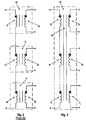
- FIG. 4 an embodiment of the invention extends the concept depicted in Fig. 1C to a four winding structure, forming a magnetic structure 76.
- Windings 116, 114, 120 and 118 carry the same current.
- a flux 112 flows through the C cores 180, 186 and through the I cores 182, 184.
- the core structure of Fig. 4 can be also constructed by using only C core members or only I core members, without departing from the spirit of the invention.
- the parallel arms 191, 192 and 193, 194 of the two C cores 180 and 186 are brought together end to end with the two coplanar I cores 182 and 184. This arrangement of the magnetic cores pieces resembles the assembled core pieces of Fig.
- the core is, once more, an unbranched, closed flux path.
- the core arms 191 - 194 penetrate a circuit board indicated as 195 on which the windings 116, 114, 120 and 118 may be printed or deposited to encircle or partially encircle the core legs.
- Fig. 5 illustrates an embodiment of the invention that is a further extension of the concept described with respect to Fig. 1C . It illustrates how the concept of this invention can be applied to any number of windings that is a multiple of two.
- the current flowing through the depicted windings 124,126,128,130,132,134, nn and mm is equal. This leads to an equal flux 138 flowing through each of the elements of the magnetic core.
- the magnetic structure 122 is a generalization of the concept described with respect to Fig. 1C .
- the core 139 can be composed entirely of C or I members or combinations of the two.
- a circuit board is indicated at 140 and is of course penetrated by the core arms 150, 151, 152, 153, 154 -mmm, nnn, which are encircled or partially encircled by the windings 124, 126, 128, 130, 132, 134 -mm, nn.
- the flux path is closed and unbranched. All windings are linked by the same flux.
- FIG. 6 an embodiment of the invention provides a mechanical configuration that offers practical application of the described concepts. It applies to a planar magnetic using a multilayer circuit board.
- the windings indicated by the dashed lines 171, 173, 175 and 177, are embedded into the multilayer circuit board 178.
- Multilayer printed circuit boards having electrically conductive buried windings at least partially encircling core portions that extend through the board are disclosed in U.S. patent No. 5,990,776 of Jitaru.
- the windings here surround the holes 181, 183, 185 and 187.
- a series of cylindrical core arms 166, 169, 170, 172 made of magnetic material are placed into the holes 181, 183, 185 and 187. These serve as the arms of the magnetic core.
- a series of plate-shaped elements 162, 168, 174 and 176 is secured by conventional means to the tops and bottoms of the cylinders 166, 169, 170, 172 in the relationship shown.
- the configuration depicted in Fig. 6 is a practical implementation of the structure depicted in Fig. 4 .
- Fig. 7 illustrates a further embodiment of the invention in which the magnetic plates 162, 168, 174 and 176 of Fig. 6 are replaced by just two magnetic plate elements 190 and 192 affixed to the cylindrical core arms 166,169,170 and 172 at their tops and bottoms.
- the advantages of using standard building elements, magnetic plates and magnetic cylinders are numerous. First of all it offers an economical solution in addressing the magnetic design for different power levels. More elements are employed as a function of the output current requirements.
- the basic cell uses a core of just two plates and two cylinders. From this cell one can extend to as many winding outputs as needed.
- layers 201, 202, 203 and 204 make up a multilayer circuit board 200.
- Magnetic core arms 210, 211 and 212 mask from view similar magnetic core arms 214, 215 and 216. Openings 220, 221 and 222 form holes through the assembled board receiving the core arms 210, 211 and 212.
- the core arms 214, 215 and 216 are similarly received in holes through the board masked from view in Fig. 8 .
- each of the core arms 210, 211, 212, 214, 215, and 216 is wound at least one winding 225 - 233. These are printed on the layers of the multilayer board and become buried windings. Magnetic core elements 240, 241, 242 and 243 extend parallel the upper and lower surfaces of the board.
- the magnetic core element 23I connects the ends of the core elements 210 and 211 in flux-conducting relation.
- the core element 234 connects the ends of the core arms 211 and 212 similarly.
- the core element 232 connects the core arms 212 and 216.
- a further, masked core element 235 lies behind the core element 234 in Fig. 8 and connects the ends of the core arms 216 and 215.
- a masked core element 236 lies behind the core element 231 connecting the core arms 214 and 215.
- the core element 233 bridges core arms 210 and 214.
- Circuit components can be seen on the upper and lower faces 241 and 242 of the board 200. At least some of these elements lie directly over or under the buried windings 225 - 233. Of those, at least certain of the components such as the components 246 and 247 are active or power components, whereas others such as 248 and 249 are passive components.
- the magnetic core like those earlier described, can be formed entirely of C or I core pieces or of a combination of C and I pieces.
- Fig. 9 illustrates schematically a preferred embodiment of the invention in which the transformer 300 is like the transformer of Fig. 3 .
- Series-connected windings 301, 302 and 303 form the primary.
- Circuitry 310, 311 and 312 treats the output of the parallel-connected windings 314, 315 and 316 that form the secondary of the transformer.
- the circuitry 310, 311 and 312 is connected between the secondary outputs and current additive nodes 318 and 319 at which the secondary windings are connected in parallel.
- the circuitry 310, 311 and 312 may be only the typical rectifying diodes or may include additional current treating elements.
Landscapes
- Engineering & Computer Science (AREA)
- Power Engineering (AREA)
- Coils Or Transformers For Communication (AREA)
- Dc-Dc Converters (AREA)
Claims (25)
- Magnetkreiselement (76), das Folgendes enthält: eine Leiterplatte (178, 195), mindestens zwei magnetflussleitende Magnetkernarme (166, 169, 170, 172, 191, 192, 193, 194), welche die Leiterplatte (195) durchdringen, mindestens zwei magnetflussleitende Magnetkernelemente (162, 168, 174, 176, 182, 184), die sich zwischen den Magnetkernarmen (191, 192, 193, 194) erstrecken, und zwar einer auf jeder Seite der Leiterplatte (195), mindestens zwei in Reihe angeschlossene Primärwicklungen (114, 116, 171, 173) auf der Leiterplatte, die mindestens einen der Arme mindestens teilweise umfangen, und mindestens zwei parallel angeschlossene Sekundärwicklungen (118, 120, 175, 177) auf der Leiterplatte, die mindestens einen der Arme mindestens teilweise umfangen, dadurch gekennzeichnet, dass jedes Kernelement (174, 176, 182, 184) die Enden eines Paares Kernarme (166, 172; 169, 170; 192, 194; 191, 193) in einer magnetflussleitenden Beziehung dergestalt verbindet, dass die Kernarme und die Kernelemente einen einzigen unverzweigten und geschlossenen Feldlinienpfad bilden, wodurch alle Primär- und Sekundärwicklungen (114, 116, 118, 120, 171, 173, 175, 177) durch denselben Magnetfluss (112) verkettet sind.
- Magnetkreiselement nach Anspruch 1, wobei die Leiterplatte eine mehrschichtige Leiterplatte (178) ist und mindestens eine der Wicklungen eine vergrabene Wicklung (171, 173, 175, 177) ist, die zwischen Schichten der mehrschichtigen Leiterplatte (178) angeordnet ist.
- Magnetkreiselement nach Anspruch 2, wobei jede der Wicklungen eine vergrabene Wicklung (171, 173, 175, 177) ist, die zwischen Schichten der mehrschichtigen Leiterplatte (178) angeordnet ist.
- Magnetkreiselement nach einem der Ansprüche 2 oder 3, das des Weiteren Schaltkreiskomponenten, einschließlich einer oder mehrerer Leistungskomponenten (246, 247), aufweist, die mindestens eine Außenseite der Leiterplatte über oder unter der mindestens einen vergrabenen Wicklung belegen.
- Magnetkreiselement nach einem der Ansprüche 1-4, wobei jede der Primärwicklungen im Wesentlichen die gleiche Anzahl an Windungen aufweist wie jede andere Sekundärwicklung.
- Magnetkreiselement nach einem der Ansprüche 1-5, wobei jede der Sekundärwicklungen im Wesentlichen die gleiche Anzahl an Windungen aufweist wie jede andere Sekundärwicklung.
- Magnetkreiselement nach einem der Ansprüche 1-6, wobei die Anzahl der Primärwicklungen die gleiche ist wie die Anzahl der Sekundärwicklungen, wobei jede Primärwicklung in einer eng gekoppelten Beziehung zu einer Sekundärwicklung gewickelt ist.
- Magnetkreiselement nach einem der Ansprüche 1-7, wobei alle Kernarme und Kernelemente aus der Gruppe ausgewählt sind, die aus C- und I-Elementen (180, 186, 182, 184) besteht.
- Magnetkreiselement nach einem der Ansprüche 1-8, das eine gerade Anzahl an Kernarmen über die Zahl von zwei hinaus enthält.
- Magnetkreiselement nach Anspruch 9, das mehr als zwei Magnetkernarme aufweist, welche die Leiterplatte durchdringen, wobei jeder Kernarm mit mindestens einer der Primär- und Sekundärwicklungen umwickelt ist.
- Magnetkreiselement nach Anspruch 10, wobei jeder Kernarm mit mindestens einer der Primärwicklungen und mindestens einer der Sekundärwicklungen umwickelt ist.
- Magnetkreiselement nach Anspruch 1, wobei die Leiterplatte eine mehrschichtige gedruckte Leiterplatte (178) der Art ist, die eine erste und eine zweite Fläche auf einer ersten und einer zweiten Seite der Leiterplatte aufweist und einen Transformator mit den Wicklungen (171, 173, 175, 177), die zwischen Schichten der Leiterplatte definiert sind, und einen Transformatorkern, der die Schichten der Leiterplatte durchdringt und um den herum die Wicklungen gewickelt sind, enthält; wobei sich mehrere, mindestens vier, Magnetkernsegmente (166, 169, 170, 172) durch die Leiterplatte hindurch von der ersten Seite zu der zweiten Seite an voneinander beabstandeten Positionen erstrecken;a) wobei die Wicklungen mehrere, mindestens vier, Wicklungen (171, 173, 175, 177) aufweisen, die jeweils mindestens teilweise ein separates der Kernsegmente (166, 169, 170, 172) umfangen, wo sich die Kernsegmente durch die Leiterplatte hindurch erstrecken;b) wobei mehrere im Wesentlichen planare erste Magnetkernelemente (162, 168) auf der ersten Seite der Leiterplatte angeordnet sind, wobei sich jedes der ersten Kernelemente zwischen einem Paar der Magnetkernsegmente (166/169, 170/172) in magnetflussleitender Beziehung dazu erstreckt, dergestalt, dass jedes Kernsegment auf der ersten Seite der Leiterplatte durch eines der im Wesentlichen planaren Kernelemente (162, 168) auf der ersten Seite der Leiterplatte in magnetflussleitender Beziehung mit einem anderen der Kernsegmente verbunden ist; undc) wobei mehrere im Wesentlichen planare zweite Magnetkernelemente (174, 176) auf der zweiten Seite der Leiterplatte angeordnet sind, wobei sich jedes der zweiten Magnetkernelemente auf der zweiten Seite der Leiterplatte zwischen einem Paar der Magnetkernsegmente (166/169, 170/172) in magnetflussleitender Beziehung dazu erstreckt.
- Verfahren zur Leistungsumwandlung zum Erzeugen einer Leistung mit hoher Amperezahl und niedriger Spannung, das Folgendes enthält:(a) Bereitstellen einer gedruckten Leiterplatte (178, 195),(b) Ausbilden von Löchern (181, 183, 185, 187) durch die gedruckte Leiterplatte hindurch,(c) Anordnen von Magnetkernarmen (166, 169, 170, 172) in den Löchern, die in der gedruckten Leiterplatte ausgebildet sind,(d) Anordnen von Magnetkernelementen (162, 168, 174, 176) in magnetflussleitender Beziehung zwischen den Kernarmen auf gegenüberliegenden Flächen der gedruckten Leiterplatte(e) Wickeln mehrerer in Reihe angeschlossener Wicklungen (171, 173) auf die Kernarme, um eine Transformator-Primärwicklung zu bilden,(f) Wickeln mehrerer parallel angeschlossener Wicklungen (175, 177) auf die Kernarme, um eine Transformator-Sekundärwicklung zu bilden,dadurch gekennzeichnet, dass mit jedem Kernelement (162, 168, 174, 176) die Enden eines Paares Kernarme (166, 169, 170, 172) in magnetflussleitender Beziehung verbunden werden, dergestalt, dass ein Transformatorkern mit einem einzigen unverzweigten geschlossenen Feldlinienpfad gebildet wird.
- Verfahren nach Anspruch 13, das des Weiteren enthält, mehrere Ausgangssignalbehandlungseinheiten am Ausgang jeder der Wicklungen, welche die Sekundärwicklung bilden, anzuordnen, wobei die Ausgangssignalbehandlungseinheiten zwischen diesen Wicklungen und einem Stromzusatzanschlusspunkt der Wicklungen angeschlossen sind.
- Verfahren nach einem der Ansprüche 13 oder 14, wobei die Schritte des Wickelns der in Reihe angeschlossenen Wicklungen und des Wickelns der parallel angeschlossenen Wicklungen das Wickeln mindestens einer der in Reihe angeschlossenen Wicklungen in eng gekoppelter Beziehung zu einer der parallel angeschlossenen Wicklungen auf jedem der Kernarme beinhalten.
- Verfahren nach einem der Ansprüche 13-15, wobei das Ausbilden von Löchern in der gedruckten Leiterplatte das Ausbilden von mehr als zwei Löchern darin enthält und wobei der Schritt des Anordnens von Magnetkernarmen in den Löchern das Anordnen von mehr als zwei Kernarmen enthält und wobei das Wickeln mehrerer in Reihe angeschlossener Wicklungen das Wickeln von mehr als zwei in Reihe angeschlossener Wicklungen auf die Kernarme enthält und das Wickeln mehrerer parallel angeschlossener Wicklungen das Wickeln von mehr als zwei parallel angeschlossenen Wicklungen auf die Kernarme enthält.
- Verfahren nach einem der Ansprüche 13-16, wobei jeder Schritt des Wickelns das Aufdrucken oder Abscheiden einer Wicklung auf einer Oberfläche der gedruckten Leiterplatte enthält, dergestalt, dass einer der Kernarme mindestens teilweise umfangen wird.
- Verfahren nach einem der Ansprüche 13-17, wobei der Schritt des Bereitstellens einer gedruckten Leiterplatte das Bereitstellen einer mehrschichtigen Leiterplatte (178) enthält und die Schritte des Wickelns mehrerer in Reihe angeschlossener und parallel angeschlossener Wicklungen das Bereitstellen mindestens mehrerer Wicklungen als vergrabene Wicklungen (171, 173, 175, 177) auf einer oder mehreren Schichtflächen zwischen den gegenüberliegenden Flächen der gedruckten Leiterplatte enthalten.
- Magnetkreiselement nach Anspruch 1,(a) wobei die Leiterplatte eine mehrschichtige Leiterplatte (178) mit einer ersten und einer zweiten Fläche ist,(b) mit einem Transformator, wobei:(A) sich jeder der Magnetkernarme (166, 169, 170, 172) durch ein Loch in der mehrschichtigen Leiterplatte von der ersten Fläche zu der zweiten Fläche erstreckt,(B) sich jedes der Magnetkernelemente (162, 168, 174, 176) entlang der ersten oder zweiten Fläche zwischen Enden der Kernarme erstreckt, um einen Magnetkreis zu schließen, der aus den Kernarmen und Kernelementen besteht,(C) mindestens zwei in Reihe angeschlossene Wicklungen (171, 173) eine Transformator-Primärwicklung bilden, die auf die mehrschichtige Leiterplatte aufgedruckt ist, wobei jede mindestens teilweise einen Kernarm umfängt,(D) mindestens zwei parallel angeschlossene Wicklungen (175, 177) eine Transformator-Sekundärwicklung bilden, die auf die mehrschichtige Leiterplatte aufgedruckt ist, wobei jede mindestens teilweise einen Kernarm umfängt, und(E) jeder Kernarm sich durch die mehrschichtige Leiterplatte hindurch erstreckt, wobei mindestens eine der Transformator-Primärwicklungen oder -Sekundärwicklungen darauf gewickelt ist.
- Magnetkreiselement nach Anspruch 19, das des Weiteren eine Transformatorsekundärwicklungs-Ausgangsverarbeitungsschaltung aufweist, die mit den parallel angeschlossenen Wicklungen verbunden ist, wobei an jede parallel angeschlossene Wicklung im Wesentlichen die gleiche Ausgangsverarbeitungsschaltung (310, 311, 312) angeschlossen ist, um den Ausgang jeder parallel angeschlossenen Wicklung in ähnlicher Weise verarbeiten zu können, wobei die Ausgangsverarbeitungsschaltungen zwischen den parallel angeschlossenen Wicklungen und einem Zwischenverbindungspunkt dieser Wicklungen angeordnet sind.
- Magnetkreiselement nach Anspruch 20, wobei der Zwischenverbindungspunkt (318, 319) zusätzlichen Strom einspeist.
- Magnetkreiselement nach einem der Ansprüche 19-21, wobei mindestens eine der Wicklungen, welche die Transformator-Primärwicklung bilden, und mindestens eine der Wicklungen, welche die Transformator-Sekundärwicklung bilden, vergrabene Wicklungen sind, die auf einer Fläche einer Schicht der mehrschichtigen Leiterplatte innerhalb der ersten und der zweiten Fläche aufgedruckt sind.
- Magnetkreiselement nach einem der Ansprüche 19-22, wobei jede der in Reihe angeschlossenen Wicklungen, welche die Transformator-Primärwicklung bilden, im Wesentlichen die gleiche Anzahl an Windungen aufweist wie jede andere der in Reihe angeschlossenen Wicklungen, welche die Transformator-Primärwicklung bilden.
- Magnetkreiselement nach einem der Ansprüche 19-23, wobei jede der parallel angeschlossenen Wicklungen, welche die Transformator-Sekundärwicklung bilden, im Wesentlichen die gleiche Anzahl an Windungen aufweist wie jede andere der parallel angeschlossenen Wicklungen, welche die Transformator-Sekundärwicklung bilden.
- Magnetkreiselement nach Anspruch 24, wobei auf jeden der Kernarme mindestens eine der in Reihe angeschlossenen Wicklungen, welche die Transformator-Primärwicklung bilden, in eng gekoppelter Beziehung zu mindestens einer der parallel angeschlossenen Wicklungen, welche die Transformator-Sekundärwicklung bilden, gewickelt ist.
Applications Claiming Priority (3)
| Application Number | Priority Date | Filing Date | Title |
|---|---|---|---|
| US37227902P | 2002-04-12 | 2002-04-12 | |
| US372279P | 2002-04-12 | ||
| PCT/CH2003/000246 WO2003088285A1 (en) | 2002-04-12 | 2003-04-11 | Low profile magnetic element |
Publications (2)
| Publication Number | Publication Date |
|---|---|
| EP1495475A1 EP1495475A1 (de) | 2005-01-12 |
| EP1495475B1 true EP1495475B1 (de) | 2008-05-07 |
Family
ID=29250830
Family Applications (1)
| Application Number | Title | Priority Date | Filing Date |
|---|---|---|---|
| EP03709549A Expired - Lifetime EP1495475B1 (de) | 2002-04-12 | 2003-04-11 | Magnetisches niederprofilelement |
Country Status (4)
| Country | Link |
|---|---|
| US (1) | US7295094B2 (de) |
| EP (1) | EP1495475B1 (de) |
| DE (1) | DE60320776D1 (de) |
| WO (1) | WO2003088285A1 (de) |
Cited By (1)
| Publication number | Priority date | Publication date | Assignee | Title |
|---|---|---|---|---|
| CN108475575A (zh) * | 2015-12-17 | 2018-08-31 | 原子能和替代能源委员会 | 包括含有被动热管理装置的至少一个感应器的电子设备 |
Families Citing this family (41)
| Publication number | Priority date | Publication date | Assignee | Title |
|---|---|---|---|---|
| SE527342C2 (sv) * | 2004-03-25 | 2006-02-14 | Schneider Electric Powerline C | Signalkopplings-/-avkopplingsanordning, system samt metoder |
| US9197132B2 (en) | 2006-12-01 | 2015-11-24 | Flextronics International Usa, Inc. | Power converter with an adaptive controller and method of operating the same |
| US7936246B2 (en) * | 2007-10-09 | 2011-05-03 | National Semiconductor Corporation | On-chip inductor for high current applications |
| US7999647B2 (en) | 2008-07-11 | 2011-08-16 | International Business Machines Corporation | Apparatus, system, and method for an integrated winding structure for a magnetic core |
| US9088216B2 (en) | 2009-01-19 | 2015-07-21 | Power Systems Technologies, Ltd. | Controller for a synchronous rectifier switch |
| JP5685815B2 (ja) * | 2009-03-16 | 2015-03-18 | Tdk株式会社 | トランスおよびスイッチング電源装置 |
| JP5257204B2 (ja) * | 2009-03-31 | 2013-08-07 | Tdk株式会社 | スイッチング電源装置 |
| US9019061B2 (en) * | 2009-03-31 | 2015-04-28 | Power Systems Technologies, Ltd. | Magnetic device formed with U-shaped core pieces and power converter employing the same |
| US8643222B2 (en) | 2009-06-17 | 2014-02-04 | Power Systems Technologies Ltd | Power adapter employing a power reducer |
| US9077248B2 (en) | 2009-06-17 | 2015-07-07 | Power Systems Technologies Ltd | Start-up circuit for a power adapter |
| US8339808B2 (en) | 2009-06-19 | 2012-12-25 | Tdk Corporation | Switching power supply unit |
| US20100321106A1 (en) * | 2009-06-23 | 2010-12-23 | Yen-Wei Hsu | Amplifier |
| US8638578B2 (en) | 2009-08-14 | 2014-01-28 | Power System Technologies, Ltd. | Power converter including a charge pump employable in a power adapter |
| US8976549B2 (en) | 2009-12-03 | 2015-03-10 | Power Systems Technologies, Ltd. | Startup circuit including first and second Schmitt triggers and power converter employing the same |
| US8406007B1 (en) | 2009-12-09 | 2013-03-26 | Universal Lighting Technologies, Inc. | Magnetic circuit board connector component |
| US9086444B2 (en) * | 2009-12-28 | 2015-07-21 | Tdk Corporation | Magnetic field detection device and current sensor |
| US9246391B2 (en) | 2010-01-22 | 2016-01-26 | Power Systems Technologies Ltd. | Controller for providing a corrected signal to a sensed peak current through a circuit element of a power converter |
| US8787043B2 (en) | 2010-01-22 | 2014-07-22 | Power Systems Technologies, Ltd. | Controller for a power converter and method of operating the same |
| WO2011116225A1 (en) | 2010-03-17 | 2011-09-22 | Power Systems Technologies, Ltd. | Control system for a power converter and method of operating the same |
| US8792257B2 (en) | 2011-03-25 | 2014-07-29 | Power Systems Technologies, Ltd. | Power converter with reduced power dissipation |
| US8823897B2 (en) * | 2011-11-29 | 2014-09-02 | Shenzhen China Star Optoelectronics Technology Co., Ltd. | Display device, liquid crystal module, and fixing structure |
| US8792256B2 (en) | 2012-01-27 | 2014-07-29 | Power Systems Technologies Ltd. | Controller for a switch and method of operating the same |
| US9190898B2 (en) | 2012-07-06 | 2015-11-17 | Power Systems Technologies, Ltd | Controller for a power converter and method of operating the same |
| US9106130B2 (en) | 2012-07-16 | 2015-08-11 | Power Systems Technologies, Inc. | Magnetic device and power converter employing the same |
| US9379629B2 (en) | 2012-07-16 | 2016-06-28 | Power Systems Technologies, Ltd. | Magnetic device and power converter employing the same |
| US9214264B2 (en) | 2012-07-16 | 2015-12-15 | Power Systems Technologies, Ltd. | Magnetic device and power converter employing the same |
| US9099232B2 (en) | 2012-07-16 | 2015-08-04 | Power Systems Technologies Ltd. | Magnetic device and power converter employing the same |
| US9240712B2 (en) | 2012-12-13 | 2016-01-19 | Power Systems Technologies Ltd. | Controller including a common current-sense device for power switches of a power converter |
| US9300206B2 (en) | 2013-11-15 | 2016-03-29 | Power Systems Technologies Ltd. | Method for estimating power of a power converter |
| US20160307695A1 (en) * | 2014-03-19 | 2016-10-20 | Ionel Jitaru | Magnetic structures for low leakage inductance and very high efficiency |
| US10128764B1 (en) | 2015-08-10 | 2018-11-13 | Vlt, Inc. | Method and apparatus for delivering power to semiconductors |
| US10468181B1 (en) | 2015-08-10 | 2019-11-05 | Vlt, Inc. | Self-aligned planar magnetic structure and method |
| US12525885B1 (en) * | 2016-04-05 | 2026-01-13 | Vicor Corporation | Planar inductive apparatus and method |
| CN107275056B (zh) * | 2017-05-12 | 2019-02-12 | 中科电力装备集团有限公司 | 一种变压器结构 |
| US10957445B2 (en) | 2017-10-05 | 2021-03-23 | Hill-Rom Services, Inc. | Caregiver and staff information system |
| DE102017223322A1 (de) * | 2017-12-20 | 2019-06-27 | Robert Bosch Gmbh | Transformatorkern und Transformator |
| US10939543B2 (en) | 2017-12-29 | 2021-03-02 | International Business Machines Corporation | Unified conductor to lower the resistance between a planar transformer and one or more inductors |
| US11848140B2 (en) * | 2019-06-11 | 2023-12-19 | Virginia Tech Intellectual Properties, Inc. | Integrated parallel matrix transformer and inductor |
| CN112104200B (zh) | 2020-02-27 | 2025-06-06 | 台达电子工业股份有限公司 | 电源模块组装结构及其组装方法 |
| US12336118B1 (en) | 2020-05-19 | 2025-06-17 | Vicor Corporation | Planar inductive apparatus and method |
| KR102607386B1 (ko) * | 2021-05-21 | 2023-11-29 | 주식회사 솔루엠 | 변압기 및 이를 포함하는 전원공급장치 |
Family Cites Families (8)
| Publication number | Priority date | Publication date | Assignee | Title |
|---|---|---|---|---|
| GB2252208B (en) * | 1991-01-24 | 1995-05-03 | Burr Brown Corp | Hybrid integrated circuit planar transformer |
| US5508673A (en) * | 1993-06-02 | 1996-04-16 | Alcatel Network Systems, Inc. | High frequency transformer apparatus |
| FI962803A0 (fi) * | 1996-07-10 | 1996-07-10 | Nokia Telecommunications Oy | Planartransformator |
| FR2752328B1 (fr) * | 1996-08-07 | 1998-10-09 | Sagem | Bobinage, notamment pour circuit haute tension de bobine d'allumage |
| US6650217B1 (en) * | 1997-03-07 | 2003-11-18 | Koninklijke Philips Electronics N.V. | Low profile magnetic component with planar winding structure having reduced conductor loss |
| AU4926099A (en) | 1998-08-21 | 2000-03-14 | Nucleus Ecopower Limited | Planar transformer |
| JP2000260639A (ja) * | 1999-03-11 | 2000-09-22 | Murata Mfg Co Ltd | コイル装置およびこれを用いたスイッチング電源装置 |
| FR2818463B1 (fr) * | 2000-12-18 | 2003-02-28 | Eisenmann France Sarl | Generateur de haute tension pour equipement de peinture electrostatique |
-
2003
- 2003-04-11 EP EP03709549A patent/EP1495475B1/de not_active Expired - Lifetime
- 2003-04-11 DE DE60320776T patent/DE60320776D1/de not_active Expired - Lifetime
- 2003-04-11 US US10/512,128 patent/US7295094B2/en not_active Expired - Lifetime
- 2003-04-11 WO PCT/CH2003/000246 patent/WO2003088285A1/en not_active Ceased
Cited By (2)
| Publication number | Priority date | Publication date | Assignee | Title |
|---|---|---|---|---|
| CN108475575A (zh) * | 2015-12-17 | 2018-08-31 | 原子能和替代能源委员会 | 包括含有被动热管理装置的至少一个感应器的电子设备 |
| CN108475575B (zh) * | 2015-12-17 | 2020-08-28 | 原子能和替代能源委员会 | 包括含有被动热管理装置的至少一个感应器的电子设备 |
Also Published As
| Publication number | Publication date |
|---|---|
| US20060006975A1 (en) | 2006-01-12 |
| EP1495475A1 (de) | 2005-01-12 |
| WO2003088285A1 (en) | 2003-10-23 |
| US7295094B2 (en) | 2007-11-13 |
| DE60320776D1 (de) | 2008-06-19 |
Similar Documents
| Publication | Publication Date | Title |
|---|---|---|
| EP1495475B1 (de) | Magnetisches niederprofilelement | |
| US6181231B1 (en) | Diamond-based transformers and power convertors | |
| US11848140B2 (en) | Integrated parallel matrix transformer and inductor | |
| US7277002B2 (en) | Electronic transformer/inductor devices and methods for making same | |
| US12170165B1 (en) | Method of manufacturing a printed circuit board with a self-aligned setback | |
| US4873757A (en) | Method of making a multilayer electrical coil | |
| CN110326207B (zh) | 具有集成磁性元件的llc谐振转换器 | |
| US12512251B2 (en) | Stacked matrix transformer | |
| US10395819B2 (en) | Multiple phase power converters having integrated magnetic cores for transformer and inductor windings | |
| US7012414B1 (en) | Vertically packaged switched-mode power converter | |
| US4201965A (en) | Inductance fabricated on a metal base printed circuit board | |
| US11894757B2 (en) | Actively cooled coil | |
| US6373736B2 (en) | Isolated converter | |
| US20180317313A1 (en) | Multi-layer printed circuit board having a printed coil and method for the production thereof | |
| US11564318B2 (en) | Voltage regulator module | |
| EP3425650B1 (de) | Modul und schaltung zur gleichstromumwandlung | |
| US11791087B2 (en) | Planar converter | |
| JP2001085248A (ja) | トランス | |
| EP2150964B1 (de) | Planarer transformer mit platten | |
| EP4066267B1 (de) | Elektrischer leistungswandler mit segmentierten wicklungen | |
| Garcia et al. | A standard design method for high frequency PCB transformers | |
| KR20190025674A (ko) | 다층 기판 | |
| US20240222002A1 (en) | Multi-layer power transformer with improved ac and dc resistance | |
| AU613211B2 (en) | High frequency matrix transformer |
Legal Events
| Date | Code | Title | Description |
|---|---|---|---|
| PUAI | Public reference made under article 153(3) epc to a published international application that has entered the european phase |
Free format text: ORIGINAL CODE: 0009012 |
|
| 17P | Request for examination filed |
Effective date: 20041006 |
|
| AK | Designated contracting states |
Kind code of ref document: A1 Designated state(s): AT BE BG CH CY CZ DE DK EE ES FI FR GB GR HU IE IT LI LU MC NL PT RO SE SI SK TR |
|
| RAP1 | Party data changed (applicant data changed or rights of an application transferred) |
Owner name: DET INTERNATIONAL HOLDING LIMITED |
|
| 17Q | First examination report despatched |
Effective date: 20060801 |
|
| GRAP | Despatch of communication of intention to grant a patent |
Free format text: ORIGINAL CODE: EPIDOSNIGR1 |
|
| RIC1 | Information provided on ipc code assigned before grant |
Ipc: H01F 27/26 20060101AFI20070928BHEP Ipc: H01F 27/28 20060101ALI20070928BHEP |
|
| GRAS | Grant fee paid |
Free format text: ORIGINAL CODE: EPIDOSNIGR3 |
|
| GRAA | (expected) grant |
Free format text: ORIGINAL CODE: 0009210 |
|
| AK | Designated contracting states |
Kind code of ref document: B1 Designated state(s): DE FR GB IT |
|
| REG | Reference to a national code |
Ref country code: GB Ref legal event code: FG4D |
|
| REF | Corresponds to: |
Ref document number: 60320776 Country of ref document: DE Date of ref document: 20080619 Kind code of ref document: P |
|
| PLBE | No opposition filed within time limit |
Free format text: ORIGINAL CODE: 0009261 |
|
| STAA | Information on the status of an ep patent application or granted ep patent |
Free format text: STATUS: NO OPPOSITION FILED WITHIN TIME LIMIT |
|
| 26N | No opposition filed |
Effective date: 20090210 |
|
| REG | Reference to a national code |
Ref country code: FR Ref legal event code: PLFP Year of fee payment: 13 |
|
| REG | Reference to a national code |
Ref country code: FR Ref legal event code: PLFP Year of fee payment: 14 |
|
| REG | Reference to a national code |
Ref country code: FR Ref legal event code: PLFP Year of fee payment: 15 |
|
| REG | Reference to a national code |
Ref country code: FR Ref legal event code: PLFP Year of fee payment: 16 |
|
| PGFP | Annual fee paid to national office [announced via postgrant information from national office to epo] |
Ref country code: FR Payment date: 20200420 Year of fee payment: 18 Ref country code: DE Payment date: 20200420 Year of fee payment: 18 |
|
| PGFP | Annual fee paid to national office [announced via postgrant information from national office to epo] |
Ref country code: IT Payment date: 20200423 Year of fee payment: 18 Ref country code: GB Payment date: 20200427 Year of fee payment: 18 |
|
| REG | Reference to a national code |
Ref country code: DE Ref legal event code: R119 Ref document number: 60320776 Country of ref document: DE |
|
| GBPC | Gb: european patent ceased through non-payment of renewal fee |
Effective date: 20210411 |
|
| PG25 | Lapsed in a contracting state [announced via postgrant information from national office to epo] |
Ref country code: DE Free format text: LAPSE BECAUSE OF NON-PAYMENT OF DUE FEES Effective date: 20211103 Ref country code: FR Free format text: LAPSE BECAUSE OF NON-PAYMENT OF DUE FEES Effective date: 20210430 Ref country code: GB Free format text: LAPSE BECAUSE OF NON-PAYMENT OF DUE FEES Effective date: 20210411 |
|
| PG25 | Lapsed in a contracting state [announced via postgrant information from national office to epo] |
Ref country code: IT Free format text: LAPSE BECAUSE OF NON-PAYMENT OF DUE FEES Effective date: 20200411 |
|
| PG25 | Lapsed in a contracting state [announced via postgrant information from national office to epo] |
Ref country code: IT Free format text: LAPSE BECAUSE OF NON-PAYMENT OF DUE FEES Effective date: 20210411 |