EP1495540B1 - Return-to-zero - und abtastimpulserzeugungsschaltungen und verfahren zur direkt-digital-aufwärtsumsetzung - Google Patents
Return-to-zero - und abtastimpulserzeugungsschaltungen und verfahren zur direkt-digital-aufwärtsumsetzung Download PDFInfo
- Publication number
- EP1495540B1 EP1495540B1 EP03716815A EP03716815A EP1495540B1 EP 1495540 B1 EP1495540 B1 EP 1495540B1 EP 03716815 A EP03716815 A EP 03716815A EP 03716815 A EP03716815 A EP 03716815A EP 1495540 B1 EP1495540 B1 EP 1495540B1
- Authority
- EP
- European Patent Office
- Prior art keywords
- output
- circuit
- differential amplifier
- pulse stream
- input
- Prior art date
- Legal status (The legal status is an assumption and is not a legal conclusion. Google has not performed a legal analysis and makes no representation as to the accuracy of the status listed.)
- Expired - Lifetime
Links
Images



Classifications
-
- H—ELECTRICITY
- H03—ELECTRONIC CIRCUITRY
- H03C—MODULATION
- H03C1/00—Amplitude modulation
- H03C1/02—Details
Definitions
- the present invention relates to signal transmission, and more particularly, relates to direct up-conversion analog signals.
- the present invention addresses the problems associated with using local oscillators by performing direct up-conversion using a novel combination of analog and digital circuitry to produce a sampling pulse, which is used to control a gated differential amplifier.
- This results in a time domain waveform that is a pulse doublet train which is amplitude modulated by the input signal to the differential amplifier.
- the pulse circuit is generated by frequency doubling, amplifying and limiting (to square up the resulting signal) a base signal one or more times, and using the resulting signals (times two, times four and so forth) to produce a short duration sampling signal repeating at the frequency of the base signal.
- the invention includes a system and method which squares an input sine wave, applies it to a frequency doubler and limiting amplifier (FDLA), and the two signals are fed to a logical NOR gate to produce a narrow sampling pulse.
- the sampling pulse is used to control the output of a gated differential amplifier.
- the output of the gated differential amplifier tracks the input (from, in one aspect, a digital to analog converter) and when the sampling pulse is not asserted, the output of the differential amplifier is pulled to zero.
- the doubled input signal is in turn applied to a FDLA to produce a times four signal which is also input to the logical NOR gate, in which aspect the sampling pulse is repeated at the frequency of the input sine wave, but has a duration of a single half cycle of eight times the frequency of the input sine wave.
- the invention is, at least in part, implemented as a Monolithic Microwave Integrated Circuit (MMIC), and in yet another aspect uses pseudomorphic high electron mobility transistors (PHEMT).
- MMIC Monolithic Microwave Integrated Circuit
- PHEMT pseudomorphic high electron mobility transistors
- the differential amplifier is controlled by gating the biasing current to the amplifier.
- the output of the differential amplifier in another aspect, is converted to unbalanced microstrip using a planar balun.
- An advantage of the present invention is that it may be implemented in a single monolithic integrated circuit without the need for external local oscillators and mixers. It is also an advantage in a wideband system that eliminating the need for local oscillators reduces the potential for in-band and near in-band re-radiation. Yet another advantage is a reduced number of circuit elements which reduces cost and power consumption.
- FIG. 1 is a block diagram of a return to zero (RTZ) circuit and sampling pulse generator in accordance with the present invention
- FIG. 2 is a time domain plot of a sample output waveform of a direct up conversion
- FIG. 3 is a plot of an output spectrum from a sample waveform after filtering by X-Band pre-selector filter
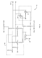
- FIG. 4 is a block diagram of an implementation of an RTZ circuit in a microchip.
- FIG. 5 is a block diagram of a clock generation circuit implementation in a microchip in accordance with one feature of the present invention.
- Direct up conversion of analog signals is of interest to radio, radar and other transmitting systems.
- Direct up-conversion can provide size, power, weight and cost benefits compared to analog up conversion using local oscillators and mixers. Elimination of local oscillators reduces the potential for in-band and near in-band local oscillator re-radiation, which is desirable in stealthy applications.
- a direct up-conversion application can be segmented into two sections: a return to zero (RTZ) sampler and a sampling pulse generator.
- RTZ return to zero
- sampling pulse generator An implementation of a return to zero (RTZ) and sampling pulse circuit in accordance with the principles of the present invention is described below.
- the RTZ uses a gated differential amplifier that tracks an input signal from an analog to digital converter at the input during a short sampling interval, and otherwise outputs zero volts.
- FIG. 1 shows a block diagram of an RTZ circuit and sampling pulse generator in accordance with the present invention.
- a sine wave input 10 is converted to a square wave by a limiting amplifier 12, producing a base pulse stream 14.
- the base pulse stream 14 is fed to a frequency doubler and limiting amplifier (FDLA) 16 producing a times two (X2) pulse stream 18 at twice the frequency of the first pulse stream 14.
- FDLA frequency doubler and limiting amplifier
- X2 times two
- the times two pulse stream 18 is fed to a second FDLA 20 producing a times four (4X) pulse stream 22.
- the three pulse streams (base 14, times two 18 and times four 22) are applied as inputs to a logical NOR circuit 24.
- the result is a sampling pulse output 25 which is a narrow pulse having a pulse width of a single half cycle of the times four pulse stream 22 and a frequency rate equal to the rate of the base pulse stream 14.
- the output 25 of the logical NOR circuit 24 is applied to a control input 28 of a gated differential amplifier 26.
- the control input 28 of the gated differential amplifier 26 When the control input 28 of the gated differential amplifier 26 is enabled, it the output of the differential amplifier 26 follows the input 27.
- the input 27 is connected to the output of a digital to analog converter.
- the RTZ and sampling pulse generator are implemented as a monolithic microwave integrated circuit (MMIC) with pseudomorphic high electron mobility transistors (PHEMT) fabricated using a 0.15 double recess fully selective (etch stop) process.
- MMIC monolithic microwave integrated circuit
- PHEMT pseudomorphic high electron mobility transistors
- etch stop 0.15 double recess fully selective process.
- the MMIC is implemented on a 101.6 um thick substrate with slot vias and incorporated 25 ohms/square TaN (Tantalum Nitride) resistors and 400 pF/mm 2 metal-insulator-metal (MIM) SiN (Silicon Nitride) capacitors.
- a time domain plot 40 of the output 34 of an RTZ circuit fabricated according to the teachings of the present invention is shown.
- a 100 MHz reference signal from a digital to analog converter (not shown) was supplied to the input of the gated differential amplifier 26, and a 2 GHz sine wave (not shown) was supplied as the input 10 to the sampling pulse generator.
- Other frequencies could be used advantageously.
- the X axis 42 is 1 nanosecond per division, and the Y axis 44 is 10 mV per division.
- the plot 46 shows the measured amplitude modulated pulse doublet time domain waveform 46 recorded using a sampling scope.
- FIG. 3 shows the output spectrum 50 of the modulated pulse doublet waveform 46 after passing it through an X-Band pre-selector filter (not shown).
- the X axis 56 is harmonic frequency at 5.0 GHz per division.
- the Y axis 58 is ten dB per division.
- Two modulation sidebands 52 and 54 are clearly evident.
- the fifth harmonic of 2 GHz is shown suppressed by eighteen dB, and the second harmonic (62 and 64) of the modulating frequency is suppressed by forty dB
- FIG 4 shows a schematic diagram of an RTZ circuit 70 as implemented in an MMIC.
- the gated differential amplifier 26 has a control input 28 which when asserted switches the control transistor 74 to supply current to the differential amplifier 26.
- the control input 28 When the control input 28 is not asserted, pull down transistors 76 and 78 pull the output of the differential amplifier 26 to zero.
- the output 80 of the differential amplifier 26 was converted to unbalanced microstrip using a planar balun (not shown).
- FIG 5 shows a schematic of a sample pulse generator circuit.
- a sine wave input 10 is applied to a circuit section 90 which squares the input sine wave to produce the base pulse stream 14, and produces the times two pulse stream 18 and the times four pulse stream 22.
- the NOR circuit 24 produces the sampling pulse 25.
- Circuit section 94 supplies a reference voltage to the NOR circuit.
Landscapes
- Amplifiers (AREA)
- Analogue/Digital Conversion (AREA)
- Stabilization Of Oscillater, Synchronisation, Frequency Synthesizers (AREA)
- Radar Systems Or Details Thereof (AREA)
Claims (15)
- Ein Verfahren für direkte digitale Aufwärtsmischung, das die folgenden Schritte beinhaltet:Anwenden mindestens eines ersten Frequenzverdoppler-und-Begrenzungsverstärkers (FDLA) auf einen ersten Impulsstrom, um einen zweiten Impulsstrom abzuleiten;Ableiten eines Abtastimpulsstroms aus einem logischen NOR von mindestens dem ersten und dem zweiten Impulsstrom;Verwenden des Abtastimpulsstroms, um einen Ausgang eines gattergesteuerten Differenzverstärkers zu aktivieren.
- Verfahren gemäß Anspruch 1, das ferner den Schritt des Ableitens eines dritten lmpulsstroms durch Anwenden eines zweiten FDLAs auf den zweiten Impulsstrom beinhaltet, wobei der dritte Impulsstrom einen weiteren Eingang an das logische NOR beinhaltet.
- Verfahren gemäß Anspruch 1 oder 2, das ferner den Schritt des Aktivierens einer Pull-down-Schaltung, welche auf den Ausgang des gattergesteuerten Differenzverstärkers angewendet wird, mit dem Abtastimpulsstrom beinhaltet.
- Verfahren gemäß einem beliebigen der Ansprüche 1 bis 3, das ferner den Schritt des Umwandelns des Ausgangs des gattergesteuerten Differenzverstärkers in einen unsymmetrischen Mikrostreifen unter der Verwendung eines planaren Symmetrietransformators beinhaltet.
- Verfahren gemäß einem beliebigen der Ansprüche 1 bis 4, das ferner den Schritt des Ableitens des ersten Impulsstroms in der Form einer Rechteckwelle durch Anwenden eines Begrenzungsverstärkers auf eine Sinuswelle beinhaltet.
- Verfahren gemäß einem beliebigen der Ansprüche 1 bis 5, das ferner den Schritt des Verwendens des Abtastimpulsstroms, um eine Stromquelle zum Vorspannen des Differenzverstärkers zu steuern, beinhaltet.
- Eine Schaltung, die Folgendes beinhaltet:mindestens einen ersten Impulsstrom;mindestens einen ersten Frequenzverdoppler- und-Begrenzungsverstärker (FDLA), der als einen Eingang mindestens den ersten Impulsstrom empfängt, und einen Ausgang, der einen zweiten Impulsstrom bereitstellt;eine Logisch-NOR-Schaltung, die als Eingang mindestens den ersten und zweiten Impulsstrom empfängt und einen Abtastimpulsstrom als einen Ausgang bereitstellt; undeinen gattergesteuerten Differenzverstärker, der den Abtastimpulsstrom als einen Steuereingang aufweist.
- Schaltung gemäß Anspruch 7, die ferner einen zweiten FDLA beinhaltet, der als einen Eingang den zweiten Impulsstrom empfängt und als einen Ausgang einen dritten lmpulsstrom, welcher einen weiteren Eingang an die Logisch-NOR-Schaltung beinhaltet, bereitstellt.
- Schaltung gemäß Anspruch 7 oder 8, wobei ein Eingang an den gattergesteuerten Differenzverstärker ein Ausgang von einem Digital-Analog-Umwandler ist.
- Schaltung gemäß einem beliebigen der Ansprüche 7 bis 9, wobei die Schaltung mindestens zum Teil als Mikrochip implementiert wird.
- Schaltung gemäß Anspruch 10, wobei die Schaltung mindestens einen PHEMT (Pseudomorphic High Electron Mobility Transistor) beinhaltet.
- Schaltung gemäß Anspruch 11, wobei der Mikrochip eine monolithische integrierte Mikrowellenschaltung beinhaltet.
- Schaltung gemäß einem beliebigen der Ansprüche 8 bis 12, die ferner einen Symmetrietransformator beinhaltet, der mit dem Ausgang des gattergesteuerten Differenzverstärkers verbunden ist, um den Ausgang in einen unsymmetrischen Mikrostreifen umzuwandeln.
- Schaltung gemäß einem beliebigen der Ansprüche 8 bis 13, die ferner einen Begrenzungsverstärker beinhaltet, welcher eine Sinuswelle als einen Eingang und das erste lmpulssignal als einen Ausgang aufweist.
- Ein System, das Folgendes beinhaltet:eine Schaltung gemäß einem beliebigen der Ansprüche 7 bis 14, wobei eine erste Impulsfolge, die auf den Eingang von mindestens dem ersten FDLA angewendet wird, eine zweite Impulsfolge an dem Ausgang von mindestens dem ersten FDLA produziert, und mindestens die erste und die zweite Impulsfolge Eingänge an die Logisch-NOR-Schaltung beinhalten, und wobei der Ausgang der Logisch-NOR-Schaltung ein Steuersignal beinhaltet; undeine Rückkehr-zu-Null-Schaltung, die einen gattergesteuerten Differenzverstärker beinhaltet, welcher einen Eingang und einen Ausgang und einen Steuereingang, welcher mit dem Steuersignal verbunden ist, aufweist, wobei der Ausgang des gattergesteuerten Differenzverstärkers dem Eingang des gattergesteuerten Differenzverstärkers folgt, wenn sich das Steuersignal in einem ersten logischen Zustand befindet, und wobei der Ausgang des gattergesteuerten Differenzverstärkers in Richtung Null gezogen wird, wenn sich das Steuersignal in einem zweiten logischen Zustand befindet.
Applications Claiming Priority (3)
| Application Number | Priority Date | Filing Date | Title |
|---|---|---|---|
| US113279 | 1993-08-27 | ||
| US10/113,279 US6617938B1 (en) | 2002-04-01 | 2002-04-01 | Return to zero and sampling pulse generating circuits and method for direct digital up conversion |
| PCT/US2003/009073 WO2003085415A2 (en) | 2002-04-01 | 2003-03-24 | Return to zero and sampling pulse generating circuits and method for direct digital up conversion |
Publications (3)
| Publication Number | Publication Date |
|---|---|
| EP1495540A2 EP1495540A2 (de) | 2005-01-12 |
| EP1495540A4 EP1495540A4 (de) | 2006-07-26 |
| EP1495540B1 true EP1495540B1 (de) | 2007-09-19 |
Family
ID=27788417
Family Applications (1)
| Application Number | Title | Priority Date | Filing Date |
|---|---|---|---|
| EP03716815A Expired - Lifetime EP1495540B1 (de) | 2002-04-01 | 2003-03-24 | Return-to-zero - und abtastimpulserzeugungsschaltungen und verfahren zur direkt-digital-aufwärtsumsetzung |
Country Status (6)
| Country | Link |
|---|---|
| US (1) | US6617938B1 (de) |
| EP (1) | EP1495540B1 (de) |
| AT (1) | ATE373893T1 (de) |
| AU (1) | AU2003220505A1 (de) |
| DE (1) | DE60316422T2 (de) |
| WO (1) | WO2003085415A2 (de) |
Families Citing this family (3)
| Publication number | Priority date | Publication date | Assignee | Title |
|---|---|---|---|---|
| EP1468307B1 (de) | 2002-01-22 | 2011-06-29 | BAE SYSTEMS Information and Electronic Systems Integration Inc. | Digital-hf-tag |
| US7560958B1 (en) * | 2003-07-14 | 2009-07-14 | National Semiconductor Corporation | Low power comparator with fast propagation delay |
| US10200222B2 (en) | 2017-01-31 | 2019-02-05 | Raytheon Company | Low cost and low frequency baseband two-tone test set using direct digital synthesizers as signal generators and a fully differential amplifier as the power combiner |
Family Cites Families (5)
| Publication number | Priority date | Publication date | Assignee | Title |
|---|---|---|---|---|
| US3731233A (en) * | 1971-11-17 | 1973-05-01 | Collins Radio Co | Minimum shift keying modulating apparatus |
| US3879663A (en) * | 1973-10-09 | 1975-04-22 | Rca Corp | Delta modulator utilizing a duty cycle circuit |
| US3959745A (en) * | 1975-06-24 | 1976-05-25 | The United States Of America As Represented By The Secretary Of The Army | Pulse amplitude modulator |
| KR960009965B1 (ko) * | 1994-04-14 | 1996-07-25 | 금성일렉트론 주식회사 | 주파수 배수 회로 |
| US5786715A (en) * | 1996-06-21 | 1998-07-28 | Sun Microsystems, Inc. | Programmable digital frequency multiplier |
-
2002
- 2002-04-01 US US10/113,279 patent/US6617938B1/en not_active Expired - Lifetime
-
2003
- 2003-03-24 WO PCT/US2003/009073 patent/WO2003085415A2/en not_active Ceased
- 2003-03-24 EP EP03716815A patent/EP1495540B1/de not_active Expired - Lifetime
- 2003-03-24 AU AU2003220505A patent/AU2003220505A1/en not_active Abandoned
- 2003-03-24 DE DE60316422T patent/DE60316422T2/de not_active Expired - Lifetime
- 2003-03-24 AT AT03716815T patent/ATE373893T1/de not_active IP Right Cessation
Also Published As
| Publication number | Publication date |
|---|---|
| AU2003220505A1 (en) | 2003-10-20 |
| AU2003220505A8 (en) | 2003-10-20 |
| WO2003085415A2 (en) | 2003-10-16 |
| ATE373893T1 (de) | 2007-10-15 |
| WO2003085415A3 (en) | 2003-11-20 |
| EP1495540A4 (de) | 2006-07-26 |
| US6617938B1 (en) | 2003-09-09 |
| EP1495540A2 (de) | 2005-01-12 |
| DE60316422D1 (de) | 2007-10-31 |
| DE60316422T2 (de) | 2008-06-19 |
Similar Documents
| Publication | Publication Date | Title |
|---|---|---|
| Razavi | Challenges in portable RF transceiver design | |
| US7010287B2 (en) | Quadrature signal generator with feedback type frequency doubler | |
| US6211708B1 (en) | Frequency doubling circuits, method, and systems including quadrature phase generators | |
| US7474885B2 (en) | Passive subharmonic mixer | |
| US20020180538A1 (en) | Local oscillator architecture to reduce transmitter pulling effect and minimize unwanted sideband | |
| CN101127746B (zh) | 用于产生混沌信号的装置和方法 | |
| CN101682299A (zh) | 双模混频器电路及方法 | |
| EP1111773B1 (de) | Halbleiterschaltung | |
| Siligaris et al. | A multichannel programmable high order frequency multiplier for channel bonding and full duplex transceivers at 60 GHz band | |
| WO1998036491A1 (en) | Voltage controlled ring oscillator frequency multiplier | |
| EP1393455B1 (de) | Quadraturabstimmung in kommunikationsempfängern | |
| Lee et al. | Reconfigurable 60-GHz radar transmitter SoC with broadband frequency tripler in 45nm SOI CMOS | |
| EP1495540B1 (de) | Return-to-zero - und abtastimpulserzeugungsschaltungen und verfahren zur direkt-digital-aufwärtsumsetzung | |
| US7805124B2 (en) | Low-loss frequency pattern generator | |
| Zhou et al. | A low-complexity FM-UWB transmitter with digital reuse and analog stacking | |
| CN101019307B (zh) | 用于超宽带频率生成的设备 | |
| US11404780B2 (en) | Phase shifter and wireless communication apparatus | |
| Camponeschi et al. | A X-Band ${\rm I}/{\rm Q} $ Upconverter in 65 nm CMOS for High Resolution FMCW Radars | |
| US20040002320A1 (en) | Square wave local oscillator technique for direct conversion receiver | |
| Flete et al. | A× 3 Sub-Sampling Mixer for a 77 GHz Automotive Radar Receiver in 28 nm FD-SOI CMOS Technology | |
| US20040178855A1 (en) | Technique for generating carrier frequencies with fast hopping capability | |
| Saoudi et al. | A multiband, spectrally-efficient impulse radio transmitter design with low-complexity CMOS pulse generator for IEEE 802.15. 4a application | |
| US20040002319A1 (en) | Harmonic boost technique for direct conversion receiver | |
| Chen et al. | A 71-86 GHz Cascaded Harmonic Enhanced Tripler with-69 dBc Fundamental and-66 dBc Second Harmonic Suppression | |
| KR102286754B1 (ko) | 폴디드 스위칭 구조의 단측파대역 주파수 혼합기 |
Legal Events
| Date | Code | Title | Description |
|---|---|---|---|
| PUAI | Public reference made under article 153(3) epc to a published international application that has entered the european phase |
Free format text: ORIGINAL CODE: 0009012 |
|
| 17P | Request for examination filed |
Effective date: 20041027 |
|
| AK | Designated contracting states |
Kind code of ref document: A2 Designated state(s): AT BE BG CH CY CZ DE DK EE ES FI FR GB GR HU IE IT LI LU MC NL PT RO SE SI SK TR |
|
| AX | Request for extension of the european patent |
Extension state: AL LT LV MK |
|
| A4 | Supplementary search report drawn up and despatched |
Effective date: 20060626 |
|
| GRAP | Despatch of communication of intention to grant a patent |
Free format text: ORIGINAL CODE: EPIDOSNIGR1 |
|
| GRAS | Grant fee paid |
Free format text: ORIGINAL CODE: EPIDOSNIGR3 |
|
| GRAA | (expected) grant |
Free format text: ORIGINAL CODE: 0009210 |
|
| AK | Designated contracting states |
Kind code of ref document: B1 Designated state(s): AT BE BG CH CY CZ DE DK EE ES FI FR GB GR HU IE IT LI LU MC NL PT RO SE SI SK TR |
|
| REG | Reference to a national code |
Ref country code: GB Ref legal event code: FG4D |
|
| REG | Reference to a national code |
Ref country code: CH Ref legal event code: EP |
|
| REF | Corresponds to: |
Ref document number: 60316422 Country of ref document: DE Date of ref document: 20071031 Kind code of ref document: P |
|
| REG | Reference to a national code |
Ref country code: IE Ref legal event code: FG4D |
|
| PG25 | Lapsed in a contracting state [announced via postgrant information from national office to epo] |
Ref country code: FI Free format text: LAPSE BECAUSE OF FAILURE TO SUBMIT A TRANSLATION OF THE DESCRIPTION OR TO PAY THE FEE WITHIN THE PRESCRIBED TIME-LIMIT Effective date: 20070919 |
|
| PG25 | Lapsed in a contracting state [announced via postgrant information from national office to epo] |
Ref country code: CH Free format text: LAPSE BECAUSE OF FAILURE TO SUBMIT A TRANSLATION OF THE DESCRIPTION OR TO PAY THE FEE WITHIN THE PRESCRIBED TIME-LIMIT Effective date: 20070919 Ref country code: AT Free format text: LAPSE BECAUSE OF FAILURE TO SUBMIT A TRANSLATION OF THE DESCRIPTION OR TO PAY THE FEE WITHIN THE PRESCRIBED TIME-LIMIT Effective date: 20070919 Ref country code: LI Free format text: LAPSE BECAUSE OF FAILURE TO SUBMIT A TRANSLATION OF THE DESCRIPTION OR TO PAY THE FEE WITHIN THE PRESCRIBED TIME-LIMIT Effective date: 20070919 |
|
| NLV1 | Nl: lapsed or annulled due to failure to fulfill the requirements of art. 29p and 29m of the patents act | ||
| PG25 | Lapsed in a contracting state [announced via postgrant information from national office to epo] |
Ref country code: BE Free format text: LAPSE BECAUSE OF FAILURE TO SUBMIT A TRANSLATION OF THE DESCRIPTION OR TO PAY THE FEE WITHIN THE PRESCRIBED TIME-LIMIT Effective date: 20070919 |
|
| REG | Reference to a national code |
Ref country code: CH Ref legal event code: PL |
|
| PG25 | Lapsed in a contracting state [announced via postgrant information from national office to epo] |
Ref country code: GR Free format text: LAPSE BECAUSE OF FAILURE TO SUBMIT A TRANSLATION OF THE DESCRIPTION OR TO PAY THE FEE WITHIN THE PRESCRIBED TIME-LIMIT Effective date: 20071220 Ref country code: NL Free format text: LAPSE BECAUSE OF FAILURE TO SUBMIT A TRANSLATION OF THE DESCRIPTION OR TO PAY THE FEE WITHIN THE PRESCRIBED TIME-LIMIT Effective date: 20070919 Ref country code: ES Free format text: LAPSE BECAUSE OF FAILURE TO SUBMIT A TRANSLATION OF THE DESCRIPTION OR TO PAY THE FEE WITHIN THE PRESCRIBED TIME-LIMIT Effective date: 20071230 |
|
| ET | Fr: translation filed | ||
| PG25 | Lapsed in a contracting state [announced via postgrant information from national office to epo] |
Ref country code: CZ Free format text: LAPSE BECAUSE OF FAILURE TO SUBMIT A TRANSLATION OF THE DESCRIPTION OR TO PAY THE FEE WITHIN THE PRESCRIBED TIME-LIMIT Effective date: 20070919 Ref country code: SK Free format text: LAPSE BECAUSE OF FAILURE TO SUBMIT A TRANSLATION OF THE DESCRIPTION OR TO PAY THE FEE WITHIN THE PRESCRIBED TIME-LIMIT Effective date: 20070919 Ref country code: PT Free format text: LAPSE BECAUSE OF FAILURE TO SUBMIT A TRANSLATION OF THE DESCRIPTION OR TO PAY THE FEE WITHIN THE PRESCRIBED TIME-LIMIT Effective date: 20080219 |
|
| PG25 | Lapsed in a contracting state [announced via postgrant information from national office to epo] |
Ref country code: SE Free format text: LAPSE BECAUSE OF FAILURE TO SUBMIT A TRANSLATION OF THE DESCRIPTION OR TO PAY THE FEE WITHIN THE PRESCRIBED TIME-LIMIT Effective date: 20071219 Ref country code: RO Free format text: LAPSE BECAUSE OF FAILURE TO SUBMIT A TRANSLATION OF THE DESCRIPTION OR TO PAY THE FEE WITHIN THE PRESCRIBED TIME-LIMIT Effective date: 20070919 |
|
| PLBE | No opposition filed within time limit |
Free format text: ORIGINAL CODE: 0009261 |
|
| STAA | Information on the status of an ep patent application or granted ep patent |
Free format text: STATUS: NO OPPOSITION FILED WITHIN TIME LIMIT |
|
| PG25 | Lapsed in a contracting state [announced via postgrant information from national office to epo] |
Ref country code: DK Free format text: LAPSE BECAUSE OF FAILURE TO SUBMIT A TRANSLATION OF THE DESCRIPTION OR TO PAY THE FEE WITHIN THE PRESCRIBED TIME-LIMIT Effective date: 20070919 |
|
| 26N | No opposition filed |
Effective date: 20080620 |
|
| PG25 | Lapsed in a contracting state [announced via postgrant information from national office to epo] |
Ref country code: MC Free format text: LAPSE BECAUSE OF NON-PAYMENT OF DUE FEES Effective date: 20080331 |
|
| PG25 | Lapsed in a contracting state [announced via postgrant information from national office to epo] |
Ref country code: IE Free format text: LAPSE BECAUSE OF NON-PAYMENT OF DUE FEES Effective date: 20080324 Ref country code: EE Free format text: LAPSE BECAUSE OF FAILURE TO SUBMIT A TRANSLATION OF THE DESCRIPTION OR TO PAY THE FEE WITHIN THE PRESCRIBED TIME-LIMIT Effective date: 20070919 |
|
| PG25 | Lapsed in a contracting state [announced via postgrant information from national office to epo] |
Ref country code: SI Free format text: LAPSE BECAUSE OF FAILURE TO SUBMIT A TRANSLATION OF THE DESCRIPTION OR TO PAY THE FEE WITHIN THE PRESCRIBED TIME-LIMIT Effective date: 20070919 |
|
| PG25 | Lapsed in a contracting state [announced via postgrant information from national office to epo] |
Ref country code: CY Free format text: LAPSE BECAUSE OF FAILURE TO SUBMIT A TRANSLATION OF THE DESCRIPTION OR TO PAY THE FEE WITHIN THE PRESCRIBED TIME-LIMIT Effective date: 20070919 |
|
| PG25 | Lapsed in a contracting state [announced via postgrant information from national office to epo] |
Ref country code: BG Free format text: LAPSE BECAUSE OF FAILURE TO SUBMIT A TRANSLATION OF THE DESCRIPTION OR TO PAY THE FEE WITHIN THE PRESCRIBED TIME-LIMIT Effective date: 20071219 |
|
| PG25 | Lapsed in a contracting state [announced via postgrant information from national office to epo] |
Ref country code: HU Free format text: LAPSE BECAUSE OF FAILURE TO SUBMIT A TRANSLATION OF THE DESCRIPTION OR TO PAY THE FEE WITHIN THE PRESCRIBED TIME-LIMIT Effective date: 20080320 Ref country code: LU Free format text: LAPSE BECAUSE OF NON-PAYMENT OF DUE FEES Effective date: 20080324 |
|
| PG25 | Lapsed in a contracting state [announced via postgrant information from national office to epo] |
Ref country code: TR Free format text: LAPSE BECAUSE OF FAILURE TO SUBMIT A TRANSLATION OF THE DESCRIPTION OR TO PAY THE FEE WITHIN THE PRESCRIBED TIME-LIMIT Effective date: 20070919 |
|
| PG25 | Lapsed in a contracting state [announced via postgrant information from national office to epo] |
Ref country code: IT Free format text: LAPSE BECAUSE OF NON-PAYMENT OF DUE FEES Effective date: 20080331 |
|
| REG | Reference to a national code |
Ref country code: GB Ref legal event code: 732E Free format text: REGISTERED BETWEEN 20110804 AND 20110810 |
|
| REG | Reference to a national code |
Ref country code: GB Ref legal event code: 732E Free format text: REGISTERED BETWEEN 20111117 AND 20111123 |
|
| REG | Reference to a national code |
Ref country code: FR Ref legal event code: TP Owner name: LATERAL RESEARCH LLC, US Effective date: 20111121 |
|
| REG | Reference to a national code |
Ref country code: DE Ref legal event code: R082 Ref document number: 60316422 Country of ref document: DE Representative=s name: MUELLER - HOFFMANN & PARTNER PATENTANWAELTE, DE Effective date: 20120216 Ref country code: DE Ref legal event code: R081 Ref document number: 60316422 Country of ref document: DE Owner name: LATERAL RESEARCH LLC, US Free format text: FORMER OWNER: BAE SYSTEMS INFORMATION AND ELECTRONIC SYSTEMS INTEGRATION INC., NASHUA, US Effective date: 20120216 Ref country code: DE Ref legal event code: R081 Ref document number: 60316422 Country of ref document: DE Owner name: LATERAL RESEARCH LLC, WILMINGTON, US Free format text: FORMER OWNER: BAE SYSTEMS INFORMATION AND ELECTRONIC SYSTEMS INTEGRATION INC., NASHUA, N.H., US Effective date: 20120216 Ref country code: DE Ref legal event code: R082 Ref document number: 60316422 Country of ref document: DE Representative=s name: MUELLER HOFFMANN & PARTNER PATENTANWAELTE MBB, DE Effective date: 20120216 |
|
| REG | Reference to a national code |
Ref country code: DE Ref legal event code: R082 Ref document number: 60316422 Country of ref document: DE Representative=s name: MUELLER - HOFFMANN & PARTNER PATENTANWAELTE, DE |
|
| REG | Reference to a national code |
Ref country code: DE Ref legal event code: R081 Ref document number: 60316422 Country of ref document: DE Owner name: LATERAL RESEARCH LLC, US Free format text: FORMER OWNER: RETRO REFLECTIVE OPTICS, LLC., PETERBOROUGH, US Effective date: 20120710 Ref country code: DE Ref legal event code: R082 Ref document number: 60316422 Country of ref document: DE Representative=s name: MUELLER - HOFFMANN & PARTNER PATENTANWAELTE, DE Effective date: 20120710 Ref country code: DE Ref legal event code: R081 Ref document number: 60316422 Country of ref document: DE Owner name: LATERAL RESEARCH LLC, WILMINGTON, US Free format text: FORMER OWNER: RETRO REFLECTIVE OPTICS, LLC., PETERBOROUGH, N.H., US Effective date: 20120710 Ref country code: DE Ref legal event code: R082 Ref document number: 60316422 Country of ref document: DE Representative=s name: MUELLER HOFFMANN & PARTNER PATENTANWAELTE MBB, DE Effective date: 20120710 |
|
| REG | Reference to a national code |
Ref country code: FR Ref legal event code: PLFP Year of fee payment: 14 |
|
| REG | Reference to a national code |
Ref country code: FR Ref legal event code: PLFP Year of fee payment: 15 |
|
| REG | Reference to a national code |
Ref country code: FR Ref legal event code: PLFP Year of fee payment: 16 |
|
| PGFP | Annual fee paid to national office [announced via postgrant information from national office to epo] |
Ref country code: FR Payment date: 20210218 Year of fee payment: 19 |
|
| PGFP | Annual fee paid to national office [announced via postgrant information from national office to epo] |
Ref country code: DE Payment date: 20210210 Year of fee payment: 19 Ref country code: GB Payment date: 20210311 Year of fee payment: 19 |
|
| REG | Reference to a national code |
Ref country code: DE Ref legal event code: R119 Ref document number: 60316422 Country of ref document: DE |
|
| GBPC | Gb: european patent ceased through non-payment of renewal fee |
Effective date: 20220324 |
|
| PG25 | Lapsed in a contracting state [announced via postgrant information from national office to epo] |
Ref country code: GB Free format text: LAPSE BECAUSE OF NON-PAYMENT OF DUE FEES Effective date: 20220324 Ref country code: FR Free format text: LAPSE BECAUSE OF NON-PAYMENT OF DUE FEES Effective date: 20220331 Ref country code: DE Free format text: LAPSE BECAUSE OF NON-PAYMENT OF DUE FEES Effective date: 20221001 |