EP1496436B1 - Verfahren und Vorrichtung zur Rücksetzung von Chipkartenvorrichtung in Stummsmodus - Google Patents
Verfahren und Vorrichtung zur Rücksetzung von Chipkartenvorrichtung in Stummsmodus Download PDFInfo
- Publication number
- EP1496436B1 EP1496436B1 EP04254046.8A EP04254046A EP1496436B1 EP 1496436 B1 EP1496436 B1 EP 1496436B1 EP 04254046 A EP04254046 A EP 04254046A EP 1496436 B1 EP1496436 B1 EP 1496436B1
- Authority
- EP
- European Patent Office
- Prior art keywords
- processor
- control logic
- status register
- mute mode
- status
- Prior art date
- Legal status (The legal status is an assumption and is not a legal conclusion. Google has not performed a legal analysis and makes no representation as to the accuracy of the status listed.)
- Expired - Lifetime
Links
Images


Classifications
-
- G—PHYSICS
- G06—COMPUTING OR CALCULATING; COUNTING
- G06F—ELECTRIC DIGITAL DATA PROCESSING
- G06F1/00—Details not covered by groups G06F3/00 - G06F13/00 and G06F21/00
- G06F1/24—Resetting means
-
- G—PHYSICS
- G06—COMPUTING OR CALCULATING; COUNTING
- G06F—ELECTRIC DIGITAL DATA PROCESSING
- G06F11/00—Error detection; Error correction; Monitoring
- G06F11/07—Responding to the occurrence of a fault, e.g. fault tolerance
- G06F11/0703—Error or fault processing not based on redundancy, i.e. by taking additional measures to deal with the error or fault not making use of redundancy in operation, in hardware, or in data representation
- G06F11/0706—Error or fault processing not based on redundancy, i.e. by taking additional measures to deal with the error or fault not making use of redundancy in operation, in hardware, or in data representation the processing taking place on a specific hardware platform or in a specific software environment
- G06F11/0745—Error or fault processing not based on redundancy, i.e. by taking additional measures to deal with the error or fault not making use of redundancy in operation, in hardware, or in data representation the processing taking place on a specific hardware platform or in a specific software environment in an input/output transactions management context
-
- G—PHYSICS
- G06—COMPUTING OR CALCULATING; COUNTING
- G06F—ELECTRIC DIGITAL DATA PROCESSING
- G06F11/00—Error detection; Error correction; Monitoring
- G06F11/07—Responding to the occurrence of a fault, e.g. fault tolerance
- G06F11/0703—Error or fault processing not based on redundancy, i.e. by taking additional measures to deal with the error or fault not making use of redundancy in operation, in hardware, or in data representation
- G06F11/0793—Remedial or corrective actions
-
- G—PHYSICS
- G06—COMPUTING OR CALCULATING; COUNTING
- G06F—ELECTRIC DIGITAL DATA PROCESSING
- G06F11/00—Error detection; Error correction; Monitoring
- G06F11/07—Responding to the occurrence of a fault, e.g. fault tolerance
- G06F11/14—Error detection or correction of the data by redundancy in operations
- G06F11/1402—Saving, restoring, recovering or retrying
- G06F11/1415—Saving, restoring, recovering or retrying at system level
- G06F11/1441—Resetting or repowering
Definitions
- the present disclosure relates generally to smart card systems, and in particular but not exclusively, relates to automatically resetting a smart card (SC) device that has entered a mute mode.
- SC smart card
- Smart cards are plastic cards having an embedded integrated circuit (IC). That IC may be a logic circuit with its associated memories, a microcontroller or microprocessor with its associated memories and software, or other type of intelligence.
- IC integrated circuit
- the IC of an SC is typically coupled to contact pads, which allow the SC to communicate or perform transactions with external devices using some type of protocol.
- external devices can include an SC reader, a host personal computer (PC), SC adapters and connectors, and the like.
- SC adapters and connectors can include an SC reader, a host personal computer (PC), SC adapters and connectors, and the like.
- SC adapters and connectors can include an SC reader, a host personal computer (PC), SC adapters and connectors, and the like.
- SCs that are available.
- the mechanical and electrical specifications of SCs are published by the International Standard Organization (ISO). For instance, the ISO 7816 protocol supports contact modes for SCs, while the ISO 14443 protocol supports contactless modes for SCs.
- ISO International Standard Organization
- USB Universal Serial Bus
- a USB smart card sometimes goes into a "mute” state or “mute” mode.
- This is a state that the SC enters when it has detected a malfunction or other abnormal condition in its operation.
- the abnormal condition can include, but not be limited to, a change in the SC's embedded code, a hacker attack, receipt of an unauthorized command, and the like.
- the SC no longer responds to further commands, and more particularly, the central processing unit (CPU) or other processor of the SC does not respond to any commands or requests presented on the USB port to which it is coupled.
- CPU central processing unit
- One technique to remove the SC from the mute mode is to perform a "hard reset" on the SC (i.e. , turn the power supplied to the SC's bus off and then turn the power back on) and start over.
- a bus reset i.e. , turn the power supplied to the SC's bus off and then turn the power back on
- USB implementations if such a bus reset is used to reset the SC's CPU, the enumeration, configuration, etc. of the SC on the bus is lost.
- Some SC applications cannot accept the lost of such data.
- WO 97/24652 describes a rest circuit for an integrated circuit.
- a watchdog timer outputs a signal if a processor fails to write to the watchdog timer.
- the processor is reset in response to this.
- US 6,439,464 describes a dual-mode integrated circuit for a smart card that can swap between a USB and ISO mode.
- a smart card apparatus comprising: a processor; a status register coupled to the processor to store status information indicative of a status associated with the processor characterized in that the processor writes to the status register to indicate transition of the processor to a mute mode just before the processor enters a mute mode; the smart card apparatus further comprising a device controller that can perform register-based and interrupt-based communication with the processor, the device controller including: control logic coupled to the processor and to the status register to check the status information stored therein to determine the status of the processor, wherein if the control logic determines that the status information indicates a mute mode associated with the processor, the control logic can initiate an interrupt-based reset signal to the processor to remove the processor from the mute mode and the device controller maintains a current configuration and state of the device controller.
- a smart card system comprising: the smart apparatus of the first aspect; a means for providing external information to the processor and for receiving information from the processor; a means for communicating between the means for providing external information and the processor; a means for receiving the external information from the means for communicating; and a means for routing and for buffering the received external information.
- a method usable for a smart card comprising: writing to a status register to indicate the transition of a processor to a mute mode just before the processor enters a mute mode; storing status information indicative of a status associated with the processor in the status register; checking the stored status information to determine the status of the processor; and if the status information indicates a mute mode associated with the processor, initiating an interrupt-based reset signal to the processor to remove the processor from the mute mode; wherein checking the stored status information and initiating a reset signal is carried out by a device controller that can perform register-based and interrupt-based communication with the processor and the current configuration and state of the device controller is maintained when the reset signal is initiated
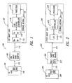
- Figure 1 is a block diagram illustrating a system in which one embodiment of the invention may be implemented.
- FIG. 2 is a block diagram illustrating another system in which one aspect of the invention may be implemented.
- FIG. 3 is a block diagram illustrating components of a SC in accordance with an embodiment of the invention.
- Figure 4 is a block diagram illustrating operation of the components of Figure 3 in more detail in accordance with an embodiment of the invention.
- FIG. 5 is a state diagram of control logic that can be implemented by the component(s) of Figures 3-4 in accordance with an embodiment of the invention.
- an embodiment of the invention provides a technique to automatically get a SC out of a mode where the SC is no longer accepting or processing commands. More particularly in one embodiment, a technique is provided to autoreset a USB SC from a mute mode.
- autoreset may be performed without having to create or define a specific USB vendor specific request (VSR) that generates a "warm reset” (i . e ., a software reset command from the USB host).
- VSR is a functionality provided by the USB specification that allows the user to define application functions in the control transfer mode that are not included in the USB specification.
- DoReset a specifically defined VSR
- the VSR is decoded by the hardware of the SC in the USB device controller and generates a hardware “warm reset” within the SC.
- a “warm reset” is different from a “cold reset,” which is the hardware reset of a device.
- Usually a "warm reset” is generated by software.
- a particularity of this "warm reset" in this embodiment is to reset only the processor and not the USB device controller.
- a VSR implementation is typically more inflexible and complex, since it often needs a specific PC driver to be loaded onto the PC host and/or SC. Moreover, such specific VSRs would require hardware modification of a SC, with the VSR having to be decoded by the hardware and the control logic has to manage its action, which may undesirably take a SC out of a standard device class.
- an embodiment of the invention provides a USB device controller (on the SC) that detects the state of the SC's CPU by polling a status register, and in the event of a mute mode, the USB device controller automatically generates a reset of the SC's CPU, thereby preserving the USB device controller configuration and setting and thus maintaining the communication with the USB host.
- a USB smart card comprises a microcontroller (such as a CPU or other processor) and a USB peripheral block on the same chip.
- the USB peripheral block is a slave to an external USB host, and is designed to respond to all standard USB or VSR requests from the USB host.
- the USB host uses a command (such as Control Mode Transfer) to control or send specific commands to a USB SC.
- a command such as Control Mode Transfer
- the USB specification has some features to ensure that the USB bus is always ready, such as Bus Reset, Single-Ended Zero (SE0), Suspend and Resume, Keep Alive, Preamble, etc.
- the role of the USB peripheral block is to then transfer data received from the USB host to the SC's CPU and memories, and vice-versa.
- the SC's CPU decodes the data, which can be a higher-level instruction or request from the host PC, or simply reads such data so that it can be used by some embedded application(s).
- the interaction between the microcontroller and the USB peripheral block requires that they always be in operation.
- the SC's CPU stops responding to requests from the USB peripheral block, which causes the USB peripheral block to stall or otherwise not respond to the USB host's requests.
- the SC has thus entered a mute mode, where as described above, a hard reset may be performed to remove the SC from the mute mode.
- a hard reset may be performed to remove the SC from the mute mode.
- another technique is to use a VSR, if one has been defined, to perform a warm reset.
- alternative or additional techniques are provided to automatically perform the reset.
- the USB smart card apparatus includes a processor and a USB device controller.
- the communication between these two entities is register-based coupled with an interrupt-based mechanism in an embodiment.
- This register interface includes a status register coupled to the processor to store status information indicative of a status associated with the processor.
- Control logic which is part of the USB device controller, is coupled to the processor and to the status register to check the status information stored therein to determine the status of the processor. If the control logic determines that the status information indicates a non-responsive state associated with the processor, the control logic can initiate an interrupt-based reset signal to the processor to remove the processor from the non-responsive state. This reset is done keeping current the configuration and state of the USB device controller.
- FIG. 1 is a block diagram illustrating a system 100 in which one embodiment of the invention may be implemented.
- a USB smart card 102 is communicatively coupled to a PC host 104 by way of a USB smart card adapter 106.
- the PC host 104 includes a USB port 108, which is used to communicatively couple the PC host 104 to the USB smart card adapter 106 via a connection 110 (such as a USB serial cable).
- a connection 112 completes the serial connection between the USB SC 102 and the PC host 104.
- Suitable USB smart card adapters are available in Schlumberger's line of E-gate smart card products, for example.
- An embodiment of the SC 102 includes D+ and D- pads 114 for communication in accordance with the USB specification, a transceiver 116 to transmit and receive information between the PC host 104 and the SC 102, a USB device controller 118, a processor 120 (such as a microcontroller, CPU, or other type of processor), and a storage medium 122 with which either one or both the processor 120 or the USB device controller 118 can communicate.
- a smart card having the autoreset features described herein may be also implemented in multi-mode smart cards, such as the USB-ISO dual-mode smart card disclosed in U.S. Patent No. 6,439,464 , which is incorporated herein by reference.
- one embodiment of the USB device controller 118 is coupled to determine the state of the processor 120 (e.g. , whether the processor 120 has entered a mute mode), such as by checking one or more status registers that is written to by the processor 120 before going to mute mode, and then takes the appropriate action to automatically reset the processor 120 from the mute mode.
- the status register(s) may comprise part of the USB device controller 118 or part of the storage medium 122.
- the storage medium 122 can itself comprise one or more machine-readable storage locations to store this status information, embedded software or code, data exchanged or to be exchanged between the SC 102 and the host PC 104, or other machine-readable instruction, data, or code.
- the storage medium 122 can be embodied as a cache, buffer, read only memory (ROM), random access memory, data register, or other suitable data repository.
- FIG 2 is a block diagram illustrating another system 200 for comparison with the system 100 of Figure 1 . More specifically, some other type (e . g ., such as an ISO 7816 smart card) smart card 202 is provided.
- the SC 202 communicates with a PC host 204 by way of a smart card reader 206.
- the PC host 204 may be a USB host that communicates with the smart card reader 206 by way of a connection 210 (such as a USB serial cable) between their USB ports 209 and 212.
- a connection 214 can comprise an ISO 7816 contact interface.
- the SC 202 includes an input/output (I/O) controller 218, a processor 220, and a storage medium 222.
- the I/O controller 218 is compliant with the ISO 7816-3 protocol, for instance.
- the SC 202 includes an I/O block 216, such as those used in an ISO 7816-compliant smart card.
- FIG. 3 is a block diagram illustrating components of a SC in accordance with an embodiment of the invention. More specifically, Figure 3 shows components of the USB device controller 118 of the SC 102 in more detail.
- the USB device controller 118 includes a serial interface engine 300 through which is routed information to be sent to the PC host 104 or received from the PC host 104.
- the serial interface engine 300 receives serial data from the transceiver 116 and parallelizes the data.
- a buffer 302 is coupled between the serial interface engine 300 and the processor 302 to store this and other information, if necessary, as the information is transferred between the processor 120 and the PC host 104.
- Control logic 304 is coupled to the buffer 302 and to the serial interface engine 300 to manage and control the flow of information between the buffer 302 and the processor 120, and to also receive (or send) data (such as the parallelized data) from the serial interface engine 302 as appropriate, so that the control logic 304 can decode this data or perform other operations related to the data.
- the communication between the USB device controller 118 and the processor 120 can be interrupt-based in an embodiment.
- control logic 304 is coupled to determine the state or mode of the processor 120 and to reset it if necessary.
- the processor 120 repeatedly writes its status information into a status register 306.
- the control logic 304 polls this status register 306, and if it detects a mute mode (such as if a bit or flag is set to binary 1), the control logic 304 initiates a reset command to the processor 120 via a reset block 308.
- the buffer 302 and the status register 306 have been indicated as comprising part of the USB device controller 118. Again, it is appreciated that such components may be separately located elsewhere on the SC 102, such as in the storage medium 122, in other embodiments.
- Figure 4 is a block diagram illustrating operation of the components of Figure 3 in more detail in accordance with an embodiment of the invention. More particularly, Figure 4 illustrates the relative interaction and connection of some of the USB device controller 118 components in more detail, and the manner in which the processor 120 may be reset. Figure 4 depicts at least three possible types of actions that may be used to reset the processor 120: a hard reset, a warm reset via use of a VSR, and an autoreset in accordance with an embodiment of the invention. The autoreset action may be used alone or in combination with either one or both the warm reset of the VSR and the hard reset.
- a hard reset e . g ., turning the power to the USB SC bus off or on, such as when initially powering up the SC 102 or when "rebooting” it
- a Power On Reset (POR) circuit 400 supplies V BUS (which may be between 4 volts and 5.5 volts supplied via the USB bus, for example) to the processor 120 to power the processor 120.
- V BUS is cut off from the processor 120 by the POR circuit 400 during the hard reset, and then subsequently re-supplied to the processor 120.
- the reset block 308 comprises an OR gate as depicted in Figure 4 , having a first input terminal 402 coupled to an output terminal of the POR circuit 400.
- the POR circuit 400 provides a binary 1 (or other suitable input signal) on the first input terminal 402 of the OR gate, for instance.
- the OR gate has an output terminal 406 coupled to the processor 120 to provide a RESET signal thereto.
- a second input terminal 404 of the OR gate is coupled to an output terminal of the control logic 304.
- the control logic 304 provides a binary 1, for example, on the second input terminal 404 of the OR gate if either one or both the warm reset of the VSR and the autoreset of an embodiment requires a reset of the processor 120.
- a VSR block 408 is provided to receive the reset VSR (such as a DoReset command) from the D+ and D- pads 114 by way of the transceiver 116, if such a VSR has been defined and has been communicated by the PC host 104 to the SC 102.
- the VSR block 408 is a circuit that decodes this VSR (as well as other VSRs that may be received), and to generate an output therefrom that instructs the control logic 304 to reset the processor 120.
- the control logic 304 can do at least some of the decoding.
- This output from the VSR block 408 (a binary 1, for example) is provided from an output terminal of the VSR block 408 to a first input terminal 410 of the control logic 304.
- the control logic 304 Upon receipt of this output from the VSR block 410, the control logic 304 provides a binary 1, for example, to the second input terminal 404 of the OR gate, which in response provides the RESET signal on its output terminal 406 to reset the processor 120.
- an embodiment of the invention provides use of the status register 306. This technique allows a reset to be automatically performed within the SC 102 itself, without needing the PC host 104 to generate a specific VSR command. Thus, when a mute mode is entered where the SC 102 stops responding to commands from the PC host 104, the communication link between the PC host 104 need not broken ⁇ the SC 102 can internally initiate a reset of the processor 120 and thereby resume communication with the PC host after reset.
- the processor 120 writes its status to the status register 306 via a WRITE line.
- the processor 120 may regularly write to a bit of the status register 306 to indicate that it is ready, busy, mute, or other status information that indicates the status of the communication link between the processor 120 and the USB device controller 118. This writing to indicate transition to a mute mode may be performed in a number of possible ways.
- the processor 120 may write (via the WRITE line) to a mute bit in the status register 306 to set that bit high to a binary 1.
- the WRITE line may comprise an enable line to enable a corresponding mute bit or other element in the status register 306 that indicates the mute mode of the processor 120. It is appreciated that instead of setting the bit high to a binary 1 or using an enable line, a mute mode may be indicated by setting a bit low to a binary 0 or by using a disable line.
- the control logic 304 polls the status register 306 to determine the status of the processor 120 and to receive the status information at its second input terminal 412. In an embodiment, this polling may be performed at suitable time intervals that are sufficiently spaced in time to be able to detect a change from one state to another, while in another embodiment and instead of polling, the status register 306 may provide updated status information to input terminal 412 of the control logic 304 only when there is a status change, for example.
- control logic 304 If the status information received by the control logic 304 at its second input terminal 412 indicates a mute mode, then the control logic 304 generates a binary 1 output, for example, for the second input terminal 404 of the OR gate, which then generates the RESET signal at its output terminal 406 to reset the processor 120. The control logic 304 then provides a signal on a RESET STATUS line that writes to the status register 306, to indicate the new status of the processor 120 (e.g. , ready, busy, or other status to indicate that the processor 120 has been taken off the mute mode).
- a RESET STATUS line that writes to the status register 306, to indicate the new status of the processor 120 (e.g. , ready, busy, or other status to indicate that the processor 120 has been taken off the mute mode).
- the status register 306 has two bits: mute bit and mute flag bit.
- the mute bit is written to by the processor 120 on the WRITE line to indicate its status, and is cleared by the control logic 304 via a CLEAR line (such as after the processor 120 has been reset from the mute mode).
- the mute flag bit is a history bit indicating that the processor 120 was in mute mode and is reset by the control logic 304.
- the mute flag bit serves as a history bit that keeps track of the previous mute state--this information can be used by the processor 120 to count the number of times that the processor 120 went through a mute mode, and thus help the processor decide to not reset after a certain number of times, three times for example.
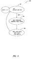
- Figure 5 is a state diagram 500 of the control logic 304 that can be implemented by the component(s) shown in Figures 3-4 in accordance with an embodiment of the invention.
- a person skilled in the art having the benefit of this disclosure can design the suitable hardware logic that will operate in accordance with the state diagram 500.
- the operations depicted in the state diagram 500 and described with respect to the other figures can be implemented in software or other machine-readable instruction stored on the machine-readable storage medium 122.
- the control logic 304 (as a state machine in one embodiment) repeatedly polls the mute bit (or flag) in the status register 306. If the processor 120 has not entered into the mute mode, then the mute bit has a value of binary 0, for example. If the processor 120 is about to enter the mute mode, then the processor 120 writes to the status register 306 to set the mute bit to a value of binary 1, for example.
- the mute bit at binary 1 causes the control logic 504 to transition to a state 504, where it initiates a reset of the processor 120. As depicted by way of example in Figure 4 , the control logic 504 initiates this reset by providing a signal to the OR gate, which then generates the RESET signal at its output terminal 406 and provides the RESET signal to the processor 120.
- the control logic 304 transitions to a state 506.
- the control logic 304 writes the new status of the processor 120 in the status register 306.
- the mute flag bit is set to binary 1 to keep the track of the previous mute state.
- the mute bit is cleared (to binary 0, for instance, or other reset status) to be able to catch the next mute state of the processor 120.
- the state of the control logic 304 returns to the state 502, where the mute bit is again repeatedly polled for processor status information.
- an aspect of the invention allows a USB SC or other type of SC to be taken out of a mute or other similar mode without necessarily having to define and use a VSR.
- This feature allows such SCs to be used for USB devices classes that allow "plug 'n play" and that are directly recognized by standard operating systems, without having to load a specific driver.
- One of many examples of such a USB class is the Chip Card Interface Device (CCID) class.
- CCID Chip Card Interface Device
- USB device controller 118 One advantage of this solution compared to previous systems based on an ISO smart card is the intelligence in the USB device controller 118. Contrary to an ISO smart card's I/O controller 218 that basically sets the direction and the interrupt of the I/O block 216, the USB device controller 118 has its own logic state machine dedicated to the USB protocol and the communication with the CPU. Because of this intelligence, there are other choices to get a CPU of a USB smart card out of the Mute mode, than having the host PC 104 or the reader software execute a special command.
- a USB smart card comprises not a single controller but two controllers on the same chip: the processor 120 (e.g. , a CPU) and the USB device controller 118.
- the processor 120 e.g. , a CPU
- the USB device controller 118 This is different than an ISO 7816-3 smart card that has only one controller: the CPU. Therefore, one embodiment of the solution to reset a USB smart card in mute mode can be done by the USB host firmware in a similar manner as the firmware of a ISO 7816-3 smart card reader for a ISO smart card, or directly by the USB device controller 118, which is sufficiently intelligent to perform the reset upon the detection of a mute condition.
- USB Universal Serial Bus
- the invention is not necessarily limited to this.
- Other aspects of the invention can have implementations based on other standards, protocols, or configurations that operate in a manner similar to USB.
Landscapes
- Engineering & Computer Science (AREA)
- Theoretical Computer Science (AREA)
- Physics & Mathematics (AREA)
- General Engineering & Computer Science (AREA)
- General Physics & Mathematics (AREA)
- Quality & Reliability (AREA)
- Information Transfer Systems (AREA)
Claims (13)
- USB-Chipkartenvorrichtung (USB = universeller serieller Bus), die Folgendes umfasst:einen ersten und einen zweiten Controller auf einer integrierten Schaltung, wobei der erste Controller ein Prozessor (120) ist und der zweite Controller ein USB-Vorrichtungscontroller (118) ist; undein Zustandsregister (306), das mit dem Prozessor gekoppelt ist, um Zustandsinformationen zu speichern, die einen Zustand anzeigen, der mit dem Prozessor in Verbindung steht, wobei der Prozessor dazu konfiguriert ist, in das Zustandsregister zu schreiben, um einen Übergang des Prozessors in einen Stummmodus anzuzeigen, bevor der Prozessor in den Stummmodus eintritt;wobei:an den USB-Host zu sendende Informationen oder von dem USB-Host zu empfangende Informationen durch den USB-Vorrichtungscontroller (118) geleitet werden;der USB-Controller (118) seine eigene logische Zustandsmaschine hat, die für das USB-Protokoll dediziert ist;der USB-Vorrichtungscontroller (118) eine Kommunikation auf Registerbasis und Interruptbasis mit dem Prozessor durchführen kann undder USB-Vorrichtungscontroller (118) Ansteuerlogik (304) aufweist, die mit dem Prozessor und dem Zustandsregister gekoppelt ist, um die darin gespeicherten Zustandsinformationen zu prüfen, um den Zustand des Prozessors zu bestimmen, wobei, wenn die Ansteuerlogik bestimmt, dass die Zustandsinformationen einen Stummmodus anzeigen, der mit dem Prozessor in Verbindung steht, die Ansteuerlogik ein Rücksetzsignal an den Prozessor initiieren kann, um den Prozessor aus dem Stummmodus zu holen.
- Vorrichtung nach Anspruch 1, die weiterhin eine Rücksetzlogik (308) umfasst, die zwischen der Ansteuerlogik (304) und dem Prozessor (120) gekoppelt ist, um dem Prozessor das Rücksetzsignal bereitzustellen.
- Vorrichtung nach Anspruch 2, die weiterhin Folgendes umfasst:eine Einschaltrücksetzschaltung (400) mit einer Ausgangsklemme, die mit einer ersten Eingangsklemme der Rücksetzlogik gekoppelt ist, um ein erstes Eingangssignal der Rücksetzlogik (308) bereitzustellen, um der Rücksetzlogik zu ermöglichen, das Rücksetzsignal als Antwort darauf zu erzeugen;eine zweite Eingangsklemme der Rücksetzlogik, die mit einer Ausgangsklemme der Ansteuerlogik (304) gekoppelt ist, um ein zweites Eingangssignal von der Ansteuerlogik zu empfangen;einen VSR-Block (VSR = vendor specific request, herstellerspezifische Anfrage) (408) zum Dekodieren einer empfangenen Anfrage, um eine benutzerdefinierte Funktion zu initiieren, und zum Bereitstellen der dekodierten Anfrage der Ansteuerlogik, um der Ansteuerlogik zu ermöglichen, das zweite Eingangssignal als Antwort darauf zu erzeugen, wobei der VSR-Block eine Ausgangsklemme hat, die mit einer ersten Eingangsklemme der Ansteuerlogik gekoppelt ist; undeine zweite Eingangsklemme der Ansteuerlogik, die mit dem Zustandsregister (306) gekoppelt ist, um die darin gespeicherten Zustandsinformationen zu empfangen, wobei die Ansteuerlogik das zweite Eingangssignal an die Rücksetzlogik erzeugen kann, wenn die Zustandsinformationen den Stummmodus anzeigen.
- Vorrichtung nach Anspruch 2 oder 3, wobei die Rücksetzlogik (304) ein ODER-Gatter umfasst.
- Vorrichtung nach einem vorhergehenden Anspruch, die weiterhin Folgendes umfasst:eine erste Leitung, die zwischen dem Prozessor (120) und dem Zustandsregister (306) gekoppelt ist, um dem Prozessor zu ermöglichen, in das Zustandsregister zu schreiben, um einen Übergang in einen Stummmodus anzuzeigen, indem die Zustandsinformationen einem Element des Zustandsregisters derart bereitgestellt werden, dass das Element den Stummmodus anzeigt;eine zweite Leitung, die zwischen der Ansteuerlogik (304) und dem Zustandsregister gekoppelt ist, um der Ansteuerlogik zu ermöglichen, Zustandsinformationen, die mit dem Prozessor in Verbindung stehen, dem Zustandsregister bereitzustellen, nachdem der Prozessor aus dem Stummmodus geholt wurde; undeine dritte Leitung, die zwischen der Ansteuerlogik und dem Zustandsregister gekoppelt ist, um das Element in dem Zustandsregister, das den Stummmodus anzeigt, zu löschen.
- Vorrichtung nach Anspruch 5, wobei das Element des Zustandsregisters (306) ein Bit umfasst, das gesetzt werden kann.
- Vorrichtung nach Anspruch 1, wobei das Zustandsregister (306) Folgendes aufweist:ein erstes Bit, das gesetzt werden kann, um anzuzeigen, dass der Prozessor (120) in den Stummmodus eintreten wird, und gelöscht werden kann, wenn der Prozessor aus dem Stummmodus geholt wurde; undein zweites Bit, das verwendet werden kann, um eine Historie von Stummmodi des Prozessors zu verfolgen.
- Vorrichtung nach Anspruch 7, die weiterhin Folgendes umfasst:eine erste Leitung, die zwischen dem Prozessor (120) und dem Zustandsregister (306) gekoppelt ist, um dem Prozessor zu ermöglichen, das erste Bit des Zustandsregisters zu setzen;eine zweite Leitung, die zwischen der Ansteuerlogik (304) und dem Zustandsregister gekoppelt ist, um der Ansteuerlogik zu ermöglichen, das zweite Bit jedes Mal zu setzen, wenn der Prozessor aus Stummmodi geholt wird; undeine dritte Leitung, die zwischen der Ansteuerlogik und dem Zustandsregister gekoppelt ist, um der Ansteuerlogik zu ermöglichen, das erste Bit zu löschen, nachdem der Prozessor aus dem Stummmodus geholt wurde.
- Vorrichtung nach einem vorhergehenden Anspruch, wobei das Zustandsregister (306) Teil des USB-Vorrichtungscontrollers (118) ist.
- Verfahren, das auf einer USB-Chipkarte (USB = universeller serieller Bus) nach Anspruch 1 ausführbar ist, wobei das Verfahren Folgendes umfasst:Speichern von Zustandsinformationen, die einen Zustand anzeigen, der mit dem Prozessor in Verbindung steht, in dem Zustandsregister, wobei der Prozessor in das Zustandsregister schreibt, um einen Übergang des Prozessors in einen Stummmodus anzuzeigen, bevor der Prozessor in den Stummmodus eintritt;Prüfen der gespeicherten Zustandsinformationen, um zu bestimmen, ob die Zustandsinformationen anzeigen, dass der Prozessor in den Stummmodus eingetreten ist; undwenn die Zustandsinformationen anzeigen, dass der Prozessor in den Stummmodus eingetreten ist, automatisches Rücksetzen des Prozessors, um ihn aus dem Stummmodus zu holen, indem ein Rücksetzsignal initiiert wird.
- Verfahren nach Anspruch 10, wobei das Speichern von Zustandsinformationen, die mit dem Zustand des Prozessors (120) in Verbindung stehen, das Setzen eines Bits vor dem Eintritt des Prozessors in den Stummmodus umfasst.
- Verfahren nach Anspruch 10, wobei das Zustandsregister (306) Teil des USB-Vorrichtungscontrollers ist.
- Maschinenlesbarer Datenträger, der auf einer USB-Chipkarte umgesetzt wird, mit darauf gespeicherten Befehlen, um das Verfahren nach einem der Ansprüche 10 bis 12 auszuführen.
Applications Claiming Priority (2)
| Application Number | Priority Date | Filing Date | Title |
|---|---|---|---|
| US614279 | 2003-07-07 | ||
| US10/614,279 US6991173B2 (en) | 2003-07-07 | 2003-07-07 | Method and apparatus for autoreset of a USB smart card device in a mute mode |
Publications (3)
| Publication Number | Publication Date |
|---|---|
| EP1496436A2 EP1496436A2 (de) | 2005-01-12 |
| EP1496436A3 EP1496436A3 (de) | 2008-11-05 |
| EP1496436B1 true EP1496436B1 (de) | 2013-09-04 |
Family
ID=33452645
Family Applications (1)
| Application Number | Title | Priority Date | Filing Date |
|---|---|---|---|
| EP04254046.8A Expired - Lifetime EP1496436B1 (de) | 2003-07-07 | 2004-07-06 | Verfahren und Vorrichtung zur Rücksetzung von Chipkartenvorrichtung in Stummsmodus |
Country Status (3)
| Country | Link |
|---|---|
| US (1) | US6991173B2 (de) |
| EP (1) | EP1496436B1 (de) |
| JP (1) | JP2005032244A (de) |
Families Citing this family (20)
| Publication number | Priority date | Publication date | Assignee | Title |
|---|---|---|---|---|
| US7117288B2 (en) * | 2003-10-24 | 2006-10-03 | Motorola Inc. | USB dynamic service switch for dual processor architecture |
| US7895384B2 (en) * | 2004-05-10 | 2011-02-22 | Sony Computer Entertainment Inc. | Portable terminal and USB device |
| US7610428B2 (en) * | 2005-12-30 | 2009-10-27 | Augmentix Corporation | System for providing a communication interface |
| US20090166421A1 (en) * | 2006-02-15 | 2009-07-02 | Dpd Patent Trust Ltd | Rfid reader / card combination to convert a contact smartcard reader to contactless |
| US8151345B1 (en) | 2007-01-25 | 2012-04-03 | Yeager C Douglas | Self-authorizing devices |
| US7651925B2 (en) * | 2007-03-01 | 2010-01-26 | Delphi Technologies, Inc. | Vacuum expansion of integrated circuits at sort |
| TW201007440A (en) * | 2008-08-01 | 2010-02-16 | Flytech Technology Co Ltd | Method of control in a multimedia data service system and system thereof |
| DE102010021086A1 (de) * | 2010-05-19 | 2011-11-24 | Vodafone Holding Gmbh | Elektronische Einrichtung und Verfahren zum Abschalten und Wiedereinschalten einer Betriebsspannung |
| KR101240486B1 (ko) * | 2011-11-24 | 2013-03-11 | 주식회사 비즈모델라인 | 유에스비 인터페이스 장치 |
| CN103325673B (zh) * | 2012-03-23 | 2016-04-20 | 万国半导体股份有限公司 | 一种支持从晶圆背面实施切割的芯片封装方法 |
| US9087158B2 (en) * | 2012-06-30 | 2015-07-21 | Intel Corporation | Explicit control message signaling |
| US11210648B2 (en) | 2012-10-17 | 2021-12-28 | Royal Bank Of Canada | Systems, methods, and devices for secure generation and processing of data sets representing pre-funded payments |
| US11080701B2 (en) | 2015-07-02 | 2021-08-03 | Royal Bank Of Canada | Secure processing of electronic payments |
| US11961075B2 (en) | 2014-10-10 | 2024-04-16 | Royal Bank Of Canada | Systems for processing electronic transactions |
| US9082119B2 (en) | 2012-10-17 | 2015-07-14 | Royal Bank of Canada. | Virtualization and secure processing of data |
| WO2015151169A1 (ja) * | 2014-03-31 | 2015-10-08 | 富士通セミコンダクター株式会社 | 制御装置及び電子機器 |
| EP3248159A4 (de) | 2015-01-19 | 2018-08-01 | Royal Bank Of Canada | Sichere verarbeitung von elektronischen zahlungen |
| US11354651B2 (en) | 2015-01-19 | 2022-06-07 | Royal Bank Of Canada | System and method for location-based token transaction processing |
| US11599879B2 (en) | 2015-07-02 | 2023-03-07 | Royal Bank Of Canada | Processing of electronic transactions |
| KR102669694B1 (ko) * | 2016-09-28 | 2024-05-28 | 삼성전자주식회사 | 서로 직렬로 연결된 스토리지 장치들 중 애플리케이션 프로세서에 직접 연결되지 않는 스토리지 장치를 리셋시키는 전자 기기 및 그것의 동작 방법 |
Family Cites Families (15)
| Publication number | Priority date | Publication date | Assignee | Title |
|---|---|---|---|---|
| US5247163A (en) * | 1990-04-20 | 1993-09-21 | Mitsubishi Denki Kabushiki Kaisha | IC card having a monitor timer and a reset signal discrimination circuit |
| EP0882258B1 (de) * | 1995-12-29 | 2000-07-26 | Advanced Micro Devices, Inc. | Rücksetzschaltung für eine batterie-getriebene integrierte schaltung und verfahren zum rücksetzen dieser integrierten schaltung |
| FR2783336B1 (fr) * | 1998-09-11 | 2001-10-12 | Schlumberger Ind Sa | Procede de transmission de donnees et carte pour une telle transmission |
| US6269443B1 (en) * | 1998-12-29 | 2001-07-31 | Intel Corporation | Method and apparatus for automatically selecting CPU clock frequency multiplier |
| FR2806505A1 (fr) * | 2000-03-15 | 2001-09-21 | Schlumberger Systems & Service | Procede de communication entre une carte a puce et une station hote |
| US6864895B1 (en) * | 2000-05-30 | 2005-03-08 | Hewlett-Packard Development Company, L.P. | Pseudo-linear frame buffer mapping system and method |
| US6978335B2 (en) * | 2000-06-30 | 2005-12-20 | 02Micro International Limited | Smart card virtual hub |
| US6439464B1 (en) | 2000-10-11 | 2002-08-27 | Stmicroelectronics, Inc. | Dual mode smart card and associated methods |
| DE10056592A1 (de) * | 2000-11-15 | 2002-05-23 | Philips Corp Intellectual Pty | Anordnung mit einem Mikroprozessor |
| US7050069B2 (en) * | 2001-03-31 | 2006-05-23 | Hewlett-Packard Development Company, L.P. | Fast clear technique for display regions having subregions |
| JP3904859B2 (ja) * | 2001-07-30 | 2007-04-11 | シャープ株式会社 | パワーオンリセット回路およびこれを備えたicカード |
| US6693637B2 (en) * | 2001-12-31 | 2004-02-17 | Intel Corporation | Method and apparatus for determining bins to be updated for polygons, including lines |
| US8933945B2 (en) * | 2002-11-27 | 2015-01-13 | Ati Technologies Ulc | Dividing work among multiple graphics pipelines using a super-tiling technique |
| US20040217966A1 (en) * | 2003-04-30 | 2004-11-04 | Lefebvre Kevin T. | Method for creating enhanced performance OpenGL display lists |
| US7218331B2 (en) * | 2003-05-13 | 2007-05-15 | Via Technologies, Inc. | Bounding box in 3D graphics |
-
2003
- 2003-07-07 US US10/614,279 patent/US6991173B2/en not_active Expired - Lifetime
-
2004
- 2004-07-01 JP JP2004195860A patent/JP2005032244A/ja active Pending
- 2004-07-06 EP EP04254046.8A patent/EP1496436B1/de not_active Expired - Lifetime
Non-Patent Citations (2)
| Title |
|---|
| "ISO/IEC 7816-3 - Information technology - Identification cards - Integrated circuit(s) cards with contacts - Part 3 : Electronic signals and transmission protocols", INTERNATIONAL STANDARD ISO/IEC,, vol. 7816-3, 15 December 1997 (1997-12-15), pages 1 - 27, XP007918490 * |
| "Universal serial bus specification - rev 2.0", UNIVERSAL SERIAL BUS SPECIFICATION,, 27 April 2000 (2000-04-27), pages 239 - 274, XP002474828 * |
Also Published As
| Publication number | Publication date |
|---|---|
| JP2005032244A (ja) | 2005-02-03 |
| US20050006483A1 (en) | 2005-01-13 |
| EP1496436A2 (de) | 2005-01-12 |
| US6991173B2 (en) | 2006-01-31 |
| EP1496436A3 (de) | 2008-11-05 |
Similar Documents
| Publication | Publication Date | Title |
|---|---|---|
| EP1496436B1 (de) | Verfahren und Vorrichtung zur Rücksetzung von Chipkartenvorrichtung in Stummsmodus | |
| EP1224559B1 (de) | Gerät und verfahren zur detektion der schnittstellensorte mit der ein peripheriegerät verbunden ist | |
| US7011247B2 (en) | Method of communication between a smart card and a host station | |
| US7739487B2 (en) | Method for booting a host device from an MMC/SD device, a host device bootable from an MMC/SD device and an MMC/SD device method a host device may booted from | |
| US6795949B2 (en) | Method and apparatus for detecting the type of interface to which a peripheral device is connected | |
| JP7179073B2 (ja) | 初期化法と関連するコントローラ、メモリデバイス、およびホスト | |
| JP4719687B2 (ja) | 着脱可能な電子回路カードのモジュール間の効率的な接続 | |
| US7664902B1 (en) | Extended SD and microSD hosts and devices with USB-like high performance packetized interface and protocol | |
| KR20110124348A (ko) | 스마트 카드 리더 | |
| US20070250564A1 (en) | Method And System For Providing A Modular Server On USB Flash Storage | |
| JP2005209204A (ja) | プロセッサを低電力状態にすることができる周辺デバイス | |
| JP2005209205A (ja) | 取外し可能媒体デバイスを有するシステムでの電力削減のシステムおよび方法 | |
| KR20050110609A (ko) | 직접 메모리 액세스에 의한 비활성 메모리 및 입출력카드의 결합 | |
| JP5386931B2 (ja) | メモリカード制御装置およびメモリカード制御方法 | |
| KR20180086129A (ko) | 정보 처리장치, 그 제어방법, 및 기억매체 | |
| EP2704017A2 (de) | Arbitrierung für ein verdrahtetes Etikett | |
| US20040008633A1 (en) | Network accessing system for computer and method of controlling the same | |
| US7124235B2 (en) | USB apparatus with switchable host/hub functions and control method thereof | |
| JP2006209643A (ja) | インタフェース回路及びそのインタフェース回路を使用したシステム装置 | |
| US7850082B1 (en) | Extended universal serial bus (USB) card reader | |
| US10318463B2 (en) | Interface controller, external electronic device, and external electronic device control method | |
| US20070106830A1 (en) | System and method to access storage inside an inactive computing device | |
| KR100764743B1 (ko) | 리셋 제어 유닛을 구비한 메모리 카드 및 그것의 리셋 제어방법 | |
| CN114546899A (zh) | Usb设备连接方法、系统及计算机可读存储介质 | |
| JP2008129836A (ja) | 処理装置 |
Legal Events
| Date | Code | Title | Description |
|---|---|---|---|
| PUAI | Public reference made under article 153(3) epc to a published international application that has entered the european phase |
Free format text: ORIGINAL CODE: 0009012 |
|
| AK | Designated contracting states |
Kind code of ref document: A2 Designated state(s): AT BE BG CH CY CZ DE DK EE ES FI FR GB GR HU IE IT LI LU MC NL PL PT RO SE SI SK TR |
|
| AX | Request for extension of the european patent |
Extension state: AL HR LT LV MK |
|
| PUAL | Search report despatched |
Free format text: ORIGINAL CODE: 0009013 |
|
| AK | Designated contracting states |
Kind code of ref document: A3 Designated state(s): AT BE BG CH CY CZ DE DK EE ES FI FR GB GR HU IE IT LI LU MC NL PL PT RO SE SI SK TR |
|
| AX | Request for extension of the european patent |
Extension state: AL HR LT LV MK |
|
| RIC1 | Information provided on ipc code assigned before grant |
Ipc: G06F 11/30 20060101AFI20041014BHEP Ipc: G06F 11/07 20060101ALI20080926BHEP |
|
| 17P | Request for examination filed |
Effective date: 20090505 |
|
| AKX | Designation fees paid |
Designated state(s): DE FR GB IT |
|
| 17Q | First examination report despatched |
Effective date: 20090616 |
|
| REG | Reference to a national code |
Ref country code: DE Ref legal event code: R079 Ref document number: 602004043221 Country of ref document: DE Free format text: PREVIOUS MAIN CLASS: G06F0011300000 Ipc: G06F0011070000 |
|
| GRAP | Despatch of communication of intention to grant a patent |
Free format text: ORIGINAL CODE: EPIDOSNIGR1 |
|
| RIC1 | Information provided on ipc code assigned before grant |
Ipc: G06F 11/14 20060101ALI20130321BHEP Ipc: G06F 11/07 20060101AFI20130321BHEP Ipc: G06F 1/24 20060101ALI20130321BHEP |
|
| INTG | Intention to grant announced |
Effective date: 20130411 |
|
| RAP1 | Party data changed (applicant data changed or rights of an application transferred) |
Owner name: STMICROELECTRONICS, INC. |
|
| GRAS | Grant fee paid |
Free format text: ORIGINAL CODE: EPIDOSNIGR3 |
|
| GRAA | (expected) grant |
Free format text: ORIGINAL CODE: 0009210 |
|
| AK | Designated contracting states |
Kind code of ref document: B1 Designated state(s): DE FR GB IT |
|
| REG | Reference to a national code |
Ref country code: GB Ref legal event code: FG4D |
|
| REG | Reference to a national code |
Ref country code: DE Ref legal event code: R096 Ref document number: 602004043221 Country of ref document: DE Effective date: 20131031 |
|
| REG | Reference to a national code |
Ref country code: DE Ref legal event code: R097 Ref document number: 602004043221 Country of ref document: DE |
|
| PLBE | No opposition filed within time limit |
Free format text: ORIGINAL CODE: 0009261 |
|
| STAA | Information on the status of an ep patent application or granted ep patent |
Free format text: STATUS: NO OPPOSITION FILED WITHIN TIME LIMIT |
|
| 26N | No opposition filed |
Effective date: 20140605 |
|
| PG25 | Lapsed in a contracting state [announced via postgrant information from national office to epo] |
Ref country code: IT Free format text: LAPSE BECAUSE OF FAILURE TO SUBMIT A TRANSLATION OF THE DESCRIPTION OR TO PAY THE FEE WITHIN THE PRESCRIBED TIME-LIMIT Effective date: 20130904 |
|
| REG | Reference to a national code |
Ref country code: DE Ref legal event code: R097 Ref document number: 602004043221 Country of ref document: DE Effective date: 20140605 |
|
| GBPC | Gb: european patent ceased through non-payment of renewal fee |
Effective date: 20140706 |
|
| PG25 | Lapsed in a contracting state [announced via postgrant information from national office to epo] |
Ref country code: GB Free format text: LAPSE BECAUSE OF NON-PAYMENT OF DUE FEES Effective date: 20140706 |
|
| REG | Reference to a national code |
Ref country code: FR Ref legal event code: PLFP Year of fee payment: 13 |
|
| REG | Reference to a national code |
Ref country code: FR Ref legal event code: PLFP Year of fee payment: 14 |
|
| REG | Reference to a national code |
Ref country code: FR Ref legal event code: PLFP Year of fee payment: 15 |
|
| REG | Reference to a national code |
Ref country code: DE Ref legal event code: R082 Ref document number: 602004043221 Country of ref document: DE Representative=s name: PAGE, WHITE & FARRER GERMANY LLP, DE |
|
| PGFP | Annual fee paid to national office [announced via postgrant information from national office to epo] |
Ref country code: FR Payment date: 20200623 Year of fee payment: 17 |
|
| PG25 | Lapsed in a contracting state [announced via postgrant information from national office to epo] |
Ref country code: FR Free format text: LAPSE BECAUSE OF NON-PAYMENT OF DUE FEES Effective date: 20210731 |
|
| PGFP | Annual fee paid to national office [announced via postgrant information from national office to epo] |
Ref country code: DE Payment date: 20230620 Year of fee payment: 20 |
|
| REG | Reference to a national code |
Ref country code: DE Ref legal event code: R071 Ref document number: 602004043221 Country of ref document: DE |