EP1496470A1 - Kombi-Chipkarte - Google Patents
Kombi-Chipkarte Download PDFInfo
- Publication number
- EP1496470A1 EP1496470A1 EP04300437A EP04300437A EP1496470A1 EP 1496470 A1 EP1496470 A1 EP 1496470A1 EP 04300437 A EP04300437 A EP 04300437A EP 04300437 A EP04300437 A EP 04300437A EP 1496470 A1 EP1496470 A1 EP 1496470A1
- Authority
- EP
- European Patent Office
- Prior art keywords
- contacts
- contact
- mode
- chip
- antenna
- Prior art date
- Legal status (The legal status is an assumption and is not a legal conclusion. Google has not performed a legal analysis and makes no representation as to the accuracy of the status listed.)
- Granted
Links
Images
Classifications
-
- G—PHYSICS
- G06—COMPUTING OR CALCULATING; COUNTING
- G06K—GRAPHICAL DATA READING; PRESENTATION OF DATA; RECORD CARRIERS; HANDLING RECORD CARRIERS
- G06K19/00—Record carriers for use with machines and with at least a part designed to carry digital markings
- G06K19/06—Record carriers for use with machines and with at least a part designed to carry digital markings characterised by the kind of the digital marking, e.g. shape, nature, code
- G06K19/067—Record carriers with conductive marks, printed circuits or semiconductor circuit elements, e.g. credit or identity cards also with resonating or responding marks without active components
- G06K19/07—Record carriers with conductive marks, printed circuits or semiconductor circuit elements, e.g. credit or identity cards also with resonating or responding marks without active components with integrated circuit chips
- G06K19/077—Constructional details, e.g. mounting of circuits in the carrier
- G06K19/07749—Constructional details, e.g. mounting of circuits in the carrier the record carrier being capable of non-contact communication, e.g. constructional details of the antenna of a non-contact smart card
- G06K19/07766—Constructional details, e.g. mounting of circuits in the carrier the record carrier being capable of non-contact communication, e.g. constructional details of the antenna of a non-contact smart card comprising at least a second communication arrangement in addition to a first non-contact communication arrangement
- G06K19/07769—Constructional details, e.g. mounting of circuits in the carrier the record carrier being capable of non-contact communication, e.g. constructional details of the antenna of a non-contact smart card comprising at least a second communication arrangement in addition to a first non-contact communication arrangement the further communication means being a galvanic interface, e.g. hybrid or mixed smart cards having a contact and a non-contact interface
-
- G—PHYSICS
- G06—COMPUTING OR CALCULATING; COUNTING
- G06K—GRAPHICAL DATA READING; PRESENTATION OF DATA; RECORD CARRIERS; HANDLING RECORD CARRIERS
- G06K19/00—Record carriers for use with machines and with at least a part designed to carry digital markings
- G06K19/06—Record carriers for use with machines and with at least a part designed to carry digital markings characterised by the kind of the digital marking, e.g. shape, nature, code
- G06K19/067—Record carriers with conductive marks, printed circuits or semiconductor circuit elements, e.g. credit or identity cards also with resonating or responding marks without active components
- G06K19/07—Record carriers with conductive marks, printed circuits or semiconductor circuit elements, e.g. credit or identity cards also with resonating or responding marks without active components with integrated circuit chips
- G06K19/0723—Record carriers with conductive marks, printed circuits or semiconductor circuit elements, e.g. credit or identity cards also with resonating or responding marks without active components with integrated circuit chips the record carrier comprising an arrangement for non-contact communication, e.g. wireless communication circuits on transponder cards, non-contact smart cards or RFIDs
-
- G—PHYSICS
- G06—COMPUTING OR CALCULATING; COUNTING
- G06K—GRAPHICAL DATA READING; PRESENTATION OF DATA; RECORD CARRIERS; HANDLING RECORD CARRIERS
- G06K7/00—Methods or arrangements for sensing record carriers, e.g. for reading patterns
- G06K7/0008—General problems related to the reading of electronic memory record carriers, independent of its reading method, e.g. power transfer
Definitions
- the present invention relates to the field of cards so-called bi-mode chips, that is to say which are likely to establish a communication with a terminal of read-write by through physical contacts as well as through inductive coupling via an antenna.
- US Pat. No. 6,168,083 discloses a card smart dual-mode, able to operate either in a mode by contacts, either in a mode without contacts.
- This document provides to select a communication session of type without contact if an AC voltage is induced in the antenna and an operating session via contacts with a read-write terminal, in the absence of a such alternating voltage and if a DC voltage is present on the physical contacts provided for this purpose.
- the map chip is provided with two interfaces, respectively mode contactless and contact mode, with a memory of the card, as well as circuits for selecting one of these interfaces. In fact, the circuits of the smart card are activated as soon as that a sufficient supply voltage level is detected by a level detection circuit, and the contactless interface is selected if another detector detects the presence of a AC voltage across the antenna.
- a disadvantage of the system provided by this document is it does not allow a failover of a contact operation to contactless operation during the same session of operation, that is to say when the selection circuit has selected one of the interfaces. We must wait for a reset the system to allow, if necessary, a switchover by a new detection phase.
- a bi-mode smart card it would be desirable, in a bi-mode smart card, to allow a switchover from a contact operation to contactless operation during the same session of communication.
- a feature is of interest particular in the case of smart cards coupled with portable devices having a battery.
- the need to reset a communication session with the chip may impose a user intervention for a switching to a non-contact mode of operation.
- a chip electronic chip card containing information the user's default is in an operation to contacts with the rest of the cell phone.
- This chip could be associated with contactless operation, for example to allow the passage of automatic turnstiles public transit using the same chip.
- a such an application is not possible with the systems known because it would force the user to cut a communication phone to reset the smart card and allow then a selection towards a mode of operation without contact.
- the present invention aims to propose a smart card dual mode that overcomes the disadvantages of known solutions. More particularly, the invention aims to propose a smart card dual mode that is likely to switch from operation to contacts to a contactless operation during the same communication session.
- the invention also aims to propose a solution which is compatible with the desired miniaturization of cards smart.
- the invention also aims to propose a solution particularly simple to implement.
- this invention provides a bi-mode smart card comprising several physical contact pads with an external reader and two pads connection to an antenna for contactless operation, and having a voltage regulator adapted to extract from a radiofrequency excitation reaching the antenna a voltage supply of the chip processing circuits, this regulator being controllable by a central circuit to be disabled in the presence of a supply voltage on contacts of the chip, so that the chip can be powered from contacts during contactless operation.
- the central control circuit exploits the results of a radio frequency presence detector on the antenna to select a contactless operating mode or a contact mode of operation.
- the circuit control unit in the absence of a radiofrequency excitation voltage and in presence of a supply voltage by contacts, deactivates the controller and initiates a communication by the contact pads, the presence detector radio frequency signal remaining activated to allow a transition to a contactless mode of operation upon arrival possible radiofrequency excitation.
- the card further comprises asynchronous transmission means directly between a demodulator of the signals received by the antenna and at least one input-output terminal with contacts.
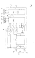
- a card 1 in a conventional manner, includes a central processing unit as well as memory (block 2, CPU + MEM) corresponding to the function classic of a smart card.
- Block 2 is connected to two pads 31 and 32 of the card 1 for receiving a supply voltage Vdd when the card is engaged in a read-write device with contacts (not shown).
- the stud 31 is for example a positive supply pad Vdd while the pad 32 is a GND ground stud.
- the smart card 1 comprises three additional contacts 33, 34 and 35 respectively to perform input / output (I / O) functions, feed a clock signal CLK from the reader and supplying a signal RST reset from the reader with contacts.
- this one also includes two pads 36 and 37 to be connected at the terminals of an antenna L in non-contact operation.
- a capacitor C connected to terminals 36 and 37 is generally integrated in card 1 and participates with the antenna L in the creation of a parallel resonant circuit capable of being excited by a electromagnetic field generated by a read-write terminal when card 1 approaches the terminal.
- the smart card 1 respects the operations planned for electromagnetic transponders according to which a carrier (for example, at 13.57 MHz) remote power is modulated to transmit data from a read-write terminal to the smart card, and that a transmission of the smart card to the terminal is performed by back-modulation at the rhythm of a subcarrier (for example, at 847 kHz).
- a bridge rectifier 4 is usually connected by its two terminals Alternative input to pads 36 and 37. Rectified output side of bridge 4, one of the terminals (for example positive) is connected at the input of a regulator 5 (RF Reg) for example linear, as well as than in the input of a demodulator 6 (Demod).
- the regulator 5 is charged to supply the rest of the board with the supply voltage necessary for its operation when this is remote powered by the electromagnetic field of a contactless terminal.
- the demodulator 6 is responsible for decoding the data transmitted by the terminal to the transponder.
- a switch K of retromodulation is generally used switching a load between the two output terminals rectified bridge 4 under control of a block 7 (Log) receiving the data to be transmitted.
- a clock signal of contactless operation to the rest of the map is extracted by a clock generation block 8 (Clock Gen) whose input is connected to one of the pads 36 and 37.
- the card 1 further comprises a circuit 9 (RF Det) for detecting the presence of an excitation radio frequency on the antenna L to detect a need for passage in contactless mode, as well as a circuit 10 (CTRL) of general order not only responsible for the selection between two modes of operation, but also the management of this operation.
- RF Det a circuit 9
- CTRL circuit 10
- the respective outputs of the regulator 5, the demodulator 6, the clock generator 8 and the radiofrequency detector 9 are sent to inputs of the control circuit 10, just as this one is connected to the pads 33, 34 and 35 of the operation with contacts.
- circuit 10 provides the data signals to the block 7 of retromodulation and exchange, with the unit circuit 2 central, data control S signals as well as power supply from terminals 31 and 32 in the contact operation. Although this is not represented, the circuit 10 exchanges signals with the different blocks of the map if it is required by their respective structures.
- a feature of the present invention is use regulator 5 only when operating without contact. As the figure shows, this one is connected in upstream of the control circuit 10 so that it does not receive a signal to regulate only when a radio frequency voltage is present in contactless operation. The rest of the time, all power is supplied by the voltage present on the terminals 31 and 32 and the regulator 5 remains disconnected. In one simplified embodiment of the regulator 5, it suffices that it does not receive signals at the output of the bridge rectifier 4, without the need for switching.
- the circuit 10 manages the different signal exchanges as follows.
- the card In the presence of radiofrequency excitation only of the smart card, that is to say while no voltage power supply does not arrive on contacts 31 and 32, the card becomes powered in the manner of an electromagnetic transponder by the regulator 5 at the same time as an excitation radio frequency is detected by the circuit 9 and that a clock is extracted from the alternative excitation by block 8.
- the map 1 then operates in contactless mode being self powered radiofrequency field and the commutations are carried out by the radiofrequency channel exclusively. In this mode of operation, the circuit 10 isolates the contacts 33, 34 and 35 during the whole session.
- the detector 9 detects the presence of a radiofrequency signal
- the block 10 who receives the information activates the demodulator 6 so to be able to exploit the signals received by the antenna.
- the regulator 5 remains deactivated, however, as long as the power supply is provided by the contacts.
- the demodulator 6 detects a data, it is transmitted by the block 10 to the CPU 2. This is then the application software who selects, according to the wishes of the application program, if one must operate then in a mode with contacts or without touching.
- the central processing unit can then process a brief interruption to validate the passage of the gate without to lose the communication, for example telephone, engaged through a contact session with the rest mobile phone.
- the radiofrequency signal detector 9 is, for for example, a detector as described in the patent application 0 903 688 of the applicant.
- An advantage of the present invention is that by providing a controllable controller upstream of the control circuit 10, it is possible to switch from a contact operation to contactless operation during the same session without risk of power conflict between the two sources possible (contacts 31 and 32, antenna terminals 36 and 37).
- a controllable circuit as is the case especially in the aforementioned US Pat. No. 6,168,083, it is not possible to switch from one mode to another during of the same session, otherwise the radio frequency power supply risk of disappearing by the external supply by studs, or Conversely.
- a smart card according to the invention may further be equipped with a transmitter asynchronous IART to transmit, without transiting to the unit unit 2, data received on the RF channel (demodulated by the block 6), to the input / output pad (s) 33 in real time.
- circuit central control unit 10 is capable of various variations and modifications that will appear to man art.
- the practical implementation of the circuit central control unit 10 is within the reach of those skilled in the art from the functional indications given above.
- the invention has been described in relation to five input / output pads for a contact operation mode, it may have a different number of contacts.
- the invention applies to all types of operation and transponder-type smart card architectures electromagnetic and all types of operation and architectures of smart cards with contacts.
Landscapes
- Engineering & Computer Science (AREA)
- Physics & Mathematics (AREA)
- General Physics & Mathematics (AREA)
- Theoretical Computer Science (AREA)
- Computer Hardware Design (AREA)
- Microelectronics & Electronic Packaging (AREA)
- Computer Networks & Wireless Communication (AREA)
- Artificial Intelligence (AREA)
- Computer Vision & Pattern Recognition (AREA)
- Near-Field Transmission Systems (AREA)
Applications Claiming Priority (2)
| Application Number | Priority Date | Filing Date | Title |
|---|---|---|---|
| FR0350311 | 2003-07-09 | ||
| FR0350311 | 2003-07-09 |
Publications (2)
| Publication Number | Publication Date |
|---|---|
| EP1496470A1 true EP1496470A1 (de) | 2005-01-12 |
| EP1496470B1 EP1496470B1 (de) | 2012-11-14 |
Family
ID=33443295
Family Applications (1)
| Application Number | Title | Priority Date | Filing Date |
|---|---|---|---|
| EP04300437A Expired - Lifetime EP1496470B1 (de) | 2003-07-09 | 2004-07-09 | Kombi-Chipkarte |
Country Status (2)
| Country | Link |
|---|---|
| US (1) | US7472834B2 (de) |
| EP (1) | EP1496470B1 (de) |
Cited By (2)
| Publication number | Priority date | Publication date | Assignee | Title |
|---|---|---|---|---|
| WO2007003429A1 (de) * | 2005-07-06 | 2007-01-11 | Giesecke & Devrient Gmbh | System mit mehreren elektronischen geräten und einem sicherheitsmodul |
| EP1955248B1 (de) * | 2005-11-30 | 2015-01-07 | Nagravision S.A. | Lernfähiges sicherheitsmodul |
Families Citing this family (19)
| Publication number | Priority date | Publication date | Assignee | Title |
|---|---|---|---|---|
| JP2006172121A (ja) * | 2004-12-15 | 2006-06-29 | Toshiba Corp | カード状記憶装置とそのアダプタ及びホスト機器 |
| CN101529262A (zh) * | 2005-05-19 | 2009-09-09 | 奈克斯测试系统公司 | 用于测试智能卡的系统及其方法 |
| JP5430050B2 (ja) * | 2005-06-24 | 2014-02-26 | フェリカネットワークス株式会社 | データ通信システム、icカード機能を実行するデバイス及びその制御方法、並びに情報処理端末 |
| FR2888976B1 (fr) * | 2005-07-25 | 2007-10-12 | Oberthur Card Syst Sa | Entite electronique avec moyens de communication par contact et a distance |
| CN101253517A (zh) * | 2005-09-02 | 2008-08-27 | Nxp股份有限公司 | 具有射频接口的数据载体 |
| US20090011706A1 (en) * | 2006-05-23 | 2009-01-08 | Innovision Research & Technology Plc | Near field RF communicators and near field communications-enabled devices |
| GB0610227D0 (en) * | 2006-05-23 | 2006-07-05 | Innovision Res & Tech Plc | Near field rf communicators and near field communications enabled devices |
| US20090159705A1 (en) * | 2007-12-24 | 2009-06-25 | Dynamics Inc. | Payment cards and devices operable to receive point-of-sale actions before point-of-sale and forward actions at point-of-sale |
| JP4640451B2 (ja) * | 2008-06-06 | 2011-03-02 | ソニー株式会社 | 接触・非接触複合icカード、通信方法、プログラム及び通信システム |
| CN101316416B (zh) * | 2008-06-20 | 2011-09-07 | 北京天语君锐科技有限公司 | 双卡双待手机芯片通信系统及通信方法 |
| KR101546071B1 (ko) * | 2009-05-21 | 2015-08-20 | 삼성전자주식회사 | 접촉식 및 비접촉식 모드를 갖는 칩 카드 및 그것의 동작 방법 |
| US8320962B2 (en) | 2009-06-05 | 2012-11-27 | Visa International Service Association | Contactless disablement |
| JP5347813B2 (ja) * | 2009-08-03 | 2013-11-20 | ソニー株式会社 | 通信装置及び通信方法 |
| KR20120011974A (ko) * | 2010-07-29 | 2012-02-09 | 삼성전자주식회사 | 복수 개의 인터페이스를 지원하는 스마트 카드 및 그것의 인터페이스 방법 |
| EP2469484A1 (de) * | 2010-12-22 | 2012-06-27 | Gemalto SA | Chipkartenempfangsvorrichtung zur Bereitstellung einer Fernkommunikation mit Schaltmitteln |
| US9483723B2 (en) | 2013-10-06 | 2016-11-01 | Tyfone, Inc. | Passive control secure transaction card |
| US9159014B2 (en) * | 2013-10-06 | 2015-10-13 | Tyfone, Inc. | Active control secure transaction card with tuned coil |
| US9208424B2 (en) | 2013-10-06 | 2015-12-08 | Tyfone, Inc. | Active control secure transaction card |
| US10643116B1 (en) | 2018-11-16 | 2020-05-05 | Graph-Tech-Usa, Llc | System and method for contactless encoding and printing of a triple interface smart card through near-field network |
Citations (5)
| Publication number | Priority date | Publication date | Assignee | Title |
|---|---|---|---|---|
| US5206495A (en) * | 1989-10-24 | 1993-04-27 | Angewandte Digital Elektronik Gmbh | Chip card |
| US6168083B1 (en) * | 1995-06-02 | 2001-01-02 | U.S. Philips Corporation | Chip-card with mode switching between contactless and contact-coupled mode |
| EP1179806A2 (de) * | 2000-07-10 | 2002-02-13 | Oki Electric Industry Co. Ltd. | Integrierte Chipkarte |
| US20020177407A1 (en) * | 2001-05-23 | 2002-11-28 | Fujitsu Limited | Portable telephone set and IC card |
| US6565007B1 (en) * | 1998-04-14 | 2003-05-20 | Angewandte Digital Elektronik | Chip card with an electronic blocking function |
Family Cites Families (3)
| Publication number | Priority date | Publication date | Assignee | Title |
|---|---|---|---|---|
| FR2787260B1 (fr) * | 1998-12-09 | 2003-01-24 | Gemplus Card Int | Dispositif electronique de communication sans contact a source d'energie auxiliaire optionnelle |
| JP2003132313A (ja) * | 2001-10-24 | 2003-05-09 | Toshiba Corp | コンビカード用lsi、コンビカード及びコンビカードの使用方法 |
| US20050035200A1 (en) * | 2003-08-11 | 2005-02-17 | Colin Hendrick | Secure smartcard sleeve |
-
2004
- 2004-07-08 US US10/886,934 patent/US7472834B2/en not_active Expired - Lifetime
- 2004-07-09 EP EP04300437A patent/EP1496470B1/de not_active Expired - Lifetime
Patent Citations (5)
| Publication number | Priority date | Publication date | Assignee | Title |
|---|---|---|---|---|
| US5206495A (en) * | 1989-10-24 | 1993-04-27 | Angewandte Digital Elektronik Gmbh | Chip card |
| US6168083B1 (en) * | 1995-06-02 | 2001-01-02 | U.S. Philips Corporation | Chip-card with mode switching between contactless and contact-coupled mode |
| US6565007B1 (en) * | 1998-04-14 | 2003-05-20 | Angewandte Digital Elektronik | Chip card with an electronic blocking function |
| EP1179806A2 (de) * | 2000-07-10 | 2002-02-13 | Oki Electric Industry Co. Ltd. | Integrierte Chipkarte |
| US20020177407A1 (en) * | 2001-05-23 | 2002-11-28 | Fujitsu Limited | Portable telephone set and IC card |
Cited By (3)
| Publication number | Priority date | Publication date | Assignee | Title |
|---|---|---|---|---|
| WO2007003429A1 (de) * | 2005-07-06 | 2007-01-11 | Giesecke & Devrient Gmbh | System mit mehreren elektronischen geräten und einem sicherheitsmodul |
| CN102722676A (zh) * | 2005-07-06 | 2012-10-10 | 德国捷德有限公司 | 具有安全模块和多个电子设备的系统 |
| EP1955248B1 (de) * | 2005-11-30 | 2015-01-07 | Nagravision S.A. | Lernfähiges sicherheitsmodul |
Also Published As
| Publication number | Publication date |
|---|---|
| EP1496470B1 (de) | 2012-11-14 |
| US7472834B2 (en) | 2009-01-06 |
| US20060086806A1 (en) | 2006-04-27 |
Similar Documents
| Publication | Publication Date | Title |
|---|---|---|
| EP1496470B1 (de) | Kombi-Chipkarte | |
| EP2341469B1 (de) | Elektronisches System und Verfahren zum Management von konkurrierenden kontaktlosen Kommunikationen im System | |
| FR2989802B1 (fr) | Carte a fonction d'affichage ayant une fonction d'authentification de securite | |
| CA2262983C (fr) | Microcircuit a fonctionnement mixte, avec ou sans contact | |
| CA2382451C (fr) | Objet portable sans contact comportant un ou plusieurs dispositifs peripheriques sans contact | |
| FR2914459A1 (fr) | Carte a microprocesseurs | |
| EP2220597B1 (de) | System mit integriertem doppeltem schaltkreis und verwendung dieses systems zum einsatz einer remote-anwendung | |
| CA2626826A1 (fr) | Procede de couplage d'un circuit integre sans contact a un composant nfc | |
| EP3001575B1 (de) | Verfahren zur steuerung des betriebs eines objekts, das in der lage ist, ohne einen kontakt mit einem lesegerät zu kommunizieren, entsprechende vorrichtung und entsprechendes objekt | |
| EP2057588A1 (de) | In kontaktloses objekt in form eines sicheren dokuments mit rfid integriertes sicheres peripheriegerät | |
| EP2070018B1 (de) | An einem zu identifizierenden objekt befestigtes rfid | |
| EP2088540A1 (de) | Tragbares Objekt mit Vermittlungsvorrichtung mit aktivierten Koppelpunkten | |
| CA2439516A1 (fr) | Objet portable sans contact comportant au moins un dispositif peripherique connecte a la meme antenne que la puce | |
| EP2107694A1 (de) | Endgerät zur Funksendung und zum Funkempfang durch induktive Kupplung | |
| FR2864297A1 (fr) | Information pleinement simultanee de variations de status pour un objet a interface duale | |
| EP1043679B1 (de) | Leser mit Einrichtung zur Bestimmung des Abstandes zwischen dem Leser und einem Transponder | |
| FR2864292A1 (fr) | Maintien en fonction pleinement simultanee d'un objet a interface duale | |
| EP1672388B1 (de) | Elektromagnetischer Transponder ohne eigenständige Energieversorgung | |
| EP4137993A1 (de) | Stromversorgung einer elektronischen vorrichtung | |
| EP1138128B1 (de) | Elektronische vorrichtung zur kontaktlosen übertragung mit wahlweiser hilfsenergiequelle | |
| FR2864296A1 (fr) | Immunite aux variations de ressources limitees, fournies a un objet a interface duale | |
| EP2202677B1 (de) | Chipkarte und mobiles Endgerät, das eine solche Karte umfasst | |
| EP2600287A1 (de) | Elektronische Vorrichtung, die Elemente umfasst, die durch verschiedene Standardprotokolle verwaltet werden, und Verwaltungsverfahren der Kommunikation zwischen diesen Elementen | |
| FR2871328A1 (fr) | Procede et systeme de communication haut debit a contacts electriques | |
| FR2864293A1 (fr) | Gestion pleinement simultanee de ressources limitees, fournies a un objet a interface duale |
Legal Events
| Date | Code | Title | Description |
|---|---|---|---|
| PUAI | Public reference made under article 153(3) epc to a published international application that has entered the european phase |
Free format text: ORIGINAL CODE: 0009012 |
|
| AK | Designated contracting states |
Kind code of ref document: A1 Designated state(s): AT BE BG CH CY CZ DE DK EE ES FI FR GB GR HU IE IT LI LU MC NL PL PT RO SE SI SK TR |
|
| AX | Request for extension of the european patent |
Extension state: AL HR LT LV MK |
|
| AKX | Designation fees paid | ||
| 17P | Request for examination filed |
Effective date: 20050711 |
|
| RBV | Designated contracting states (corrected) |
Designated state(s): DE FR GB IT |
|
| REG | Reference to a national code |
Ref country code: DE Ref legal event code: 8566 |
|
| GRAP | Despatch of communication of intention to grant a patent |
Free format text: ORIGINAL CODE: EPIDOSNIGR1 |
|
| GRAS | Grant fee paid |
Free format text: ORIGINAL CODE: EPIDOSNIGR3 |
|
| GRAA | (expected) grant |
Free format text: ORIGINAL CODE: 0009210 |
|
| AK | Designated contracting states |
Kind code of ref document: B1 Designated state(s): DE FR GB IT |
|
| REG | Reference to a national code |
Ref country code: GB Ref legal event code: FG4D Free format text: NOT ENGLISH |
|
| REG | Reference to a national code |
Ref country code: DE Ref legal event code: R096 Ref document number: 602004040015 Country of ref document: DE Effective date: 20130103 |
|
| PG25 | Lapsed in a contracting state [announced via postgrant information from national office to epo] |
Ref country code: IT Free format text: LAPSE BECAUSE OF FAILURE TO SUBMIT A TRANSLATION OF THE DESCRIPTION OR TO PAY THE FEE WITHIN THE PRESCRIBED TIME-LIMIT Effective date: 20121114 |
|
| PLBE | No opposition filed within time limit |
Free format text: ORIGINAL CODE: 0009261 |
|
| STAA | Information on the status of an ep patent application or granted ep patent |
Free format text: STATUS: NO OPPOSITION FILED WITHIN TIME LIMIT |
|
| 26N | No opposition filed |
Effective date: 20130815 |
|
| PGFP | Annual fee paid to national office [announced via postgrant information from national office to epo] |
Ref country code: FR Payment date: 20130722 Year of fee payment: 10 |
|
| REG | Reference to a national code |
Ref country code: DE Ref legal event code: R097 Ref document number: 602004040015 Country of ref document: DE Effective date: 20130815 |
|
| GBPC | Gb: european patent ceased through non-payment of renewal fee |
Effective date: 20130709 |
|
| PG25 | Lapsed in a contracting state [announced via postgrant information from national office to epo] |
Ref country code: GB Free format text: LAPSE BECAUSE OF NON-PAYMENT OF DUE FEES Effective date: 20130709 |
|
| REG | Reference to a national code |
Ref country code: FR Ref legal event code: ST Effective date: 20150331 |
|
| PG25 | Lapsed in a contracting state [announced via postgrant information from national office to epo] |
Ref country code: FR Free format text: LAPSE BECAUSE OF NON-PAYMENT OF DUE FEES Effective date: 20140731 |
|
| PGFP | Annual fee paid to national office [announced via postgrant information from national office to epo] |
Ref country code: DE Payment date: 20230620 Year of fee payment: 20 |