EP1496690A2 - Bildgeber und Flimmerreduktionsverfahren - Google Patents
Bildgeber und Flimmerreduktionsverfahren Download PDFInfo
- Publication number
- EP1496690A2 EP1496690A2 EP04254041A EP04254041A EP1496690A2 EP 1496690 A2 EP1496690 A2 EP 1496690A2 EP 04254041 A EP04254041 A EP 04254041A EP 04254041 A EP04254041 A EP 04254041A EP 1496690 A2 EP1496690 A2 EP 1496690A2
- Authority
- EP
- European Patent Office
- Prior art keywords
- flicker
- seconds
- shutter
- value
- case
- Prior art date
- Legal status (The legal status is an assumption and is not a legal conclusion. Google has not performed a legal analysis and makes no representation as to the accuracy of the status listed.)
- Ceased
Links
Images


Classifications
-
- H—ELECTRICITY
- H04—ELECTRIC COMMUNICATION TECHNIQUE
- H04N—PICTORIAL COMMUNICATION, e.g. TELEVISION
- H04N23/00—Cameras or camera modules comprising electronic image sensors; Control thereof
- H04N23/70—Circuitry for compensating brightness variation in the scene
-
- H—ELECTRICITY
- H04—ELECTRIC COMMUNICATION TECHNIQUE
- H04N—PICTORIAL COMMUNICATION, e.g. TELEVISION
- H04N23/00—Cameras or camera modules comprising electronic image sensors; Control thereof
- H04N23/70—Circuitry for compensating brightness variation in the scene
- H04N23/745—Detection of flicker frequency or suppression of flicker wherein the flicker is caused by illumination, e.g. due to fluorescent tube illumination or pulsed LED illumination
-
- H—ELECTRICITY
- H04—ELECTRIC COMMUNICATION TECHNIQUE
- H04N—PICTORIAL COMMUNICATION, e.g. TELEVISION
- H04N23/00—Cameras or camera modules comprising electronic image sensors; Control thereof
- H04N23/70—Circuitry for compensating brightness variation in the scene
- H04N23/76—Circuitry for compensating brightness variation in the scene by influencing the image signals
-
- H—ELECTRICITY
- H04—ELECTRIC COMMUNICATION TECHNIQUE
- H04N—PICTORIAL COMMUNICATION, e.g. TELEVISION
- H04N25/00—Circuitry of solid-state image sensors [SSIS]; Control thereof
- H04N25/50—Control of the SSIS exposure
- H04N25/57—Control of the dynamic range
Definitions
- the present invention relates to imaging apparatus, such as for example, video cameras or digital still cameras, in which an XY address scanning-type imaging device is used.
- an intensity change with respect to time that is, so-called fluorescent lamp flicker, occurs in the video signal of the photographed output due to the difference between the frequency (twice the commercial AC power-supply frequency) of the luminance change (change in the amount of light) of the fluorescent lamp and the vertical synchronization frequency (imaging frequency) of the camera.
- the amount of exposure differs even with the same exposure time. Furthermore, when the exposure time is shorter than 1/60 seconds (when it is not 1/100 seconds, as will be described later), in periods b1, b2, and b3, the amount of exposure differs even with the same exposure time.
- the exposure timing with respect to the luminance change of the fluorescent lamp returns to the original timing every three fields, and therefore, the intensity change due to flicker repeats every three fields. That is, the luminance ratio of each field changes depending on the exposure period, but the flicker period does not change.
- the vertical synchronization frequency (the frame frequency in this case) is 30 Hz
- the intensity change is repeated every three frames.
- the fluorescent lamp usually, a plurality of fluorescent substances, for example, red, green, and blue fluorescent substances, are used to emit white light.
- each of these fluorescent substances has specific persistence characteristics and emits light in a decaying manner with individual persistence characteristics in the period from the stopping of discharge, which exists in the period of the luminance change, up to the start of the next discharge. For this reason, in this period, since the light, which is initially white light, gradually decays while changing its hue, if the exposure timing is shifted in the manner described above, not only does the intensity change but a hue change also occurs.
- the fluorescent lamp has specific spectral characteristics such that a strong peak exists at a specific wavelength, variation components of the signal differs depending on the color.
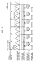
- the exposure time is set to 1/100 seconds, which is the period of the luminance change of the fluorescent lamp, as shown in the bottommost portion of Fig. 1, the amount of exposure becomes constant regardless of the exposure timing, and flicker does not occur.
- the exposure timing for each pixel is shifted in sequence by an amount corresponding to one period of the reading clock (pixel clock) in the horizontal direction of the picture plane, and the exposure timing differs in all the pixels.
- flicker cannot be suppressed sufficiently.
- Fig. 2 shows this situation.
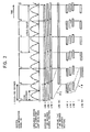
- the exposure timing of each pixel is shifted in sequence, but one horizontal period is sufficiently short when compared to the period of the luminance change of the fluorescent lamp.
- the exposure timing of each line in the vertical direction of the picture plane is shown. In practical terms, the above assumption does not cause problems to occur.
- the exposure timing differs for each line (F0 indicates the situation for a particular field), and the amount of exposure differs in each line.
- F0 indicates the situation for a particular field
- the amount of exposure differs in each line.
- an intensity change and a color change due to flicker occur not only between fields but also inside fields, and the changes appear as a stripe pattern (the direction of the stripes themselves is the horizontal direction, and the direction of the change of the stripe is the vertical direction) on the picture plane.
- this stripe pattern corresponds to five periods (five wavelengths) in three fields (three frames), and when viewed continuously, it appears to flow in the vertical direction.
- Figs. 3 and 4 show only the intensity change due to flicker.
- the above-described color change is added, and the image quality is deteriorated considerably.
- color flicker becomes more noticeable as the shutter speed becomes higher (the exposure time becomes shorter), and in the XY address scanning-type imaging apparatus, the influence of the color flicker appears within the picture plane. Consequently, the deterioration of the image quality becomes more pronounced.
- the NTSC system (the vertical synchronization frequency is 60 Hz) and the PAL system (the vertical synchronization frequency is 50 Hz), which correspond to a broadcasting system, are known.
- Most recent video cameras are compatible with both the NTSC system and the PAL system. It is common practice that, when video cameras are shipped from the factory, they are electrically set to either the NTSC system or the PAL system according to the shipment destination.
- the commercial AC power-supply frequency is 50 Hz in some areas of Japan and in some countries or areas of the world, and it is 60 Hz in other areas of Japan and in other countries or areas of the world.
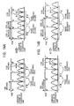
- Case 1 of Fig. 5A shows a case in which a subject is photographed by a CMOS imaging apparatus of the NTSC system under the illumination of a fluorescent lamp in an area where the power-supply frequency is 50 Hz.
- Case 2 of Fig. 5B shows a case in which a subject is photographed by a CMOS imaging apparatus of the PAL system under the illumination of a fluorescent lamp in an area where the power-supply frequency is 60 Hz.
- the period of the luminance change of the fluorescent lamp is 1/120 seconds. Consequently, during the normal shutter time, where the exposure time is 1/50 seconds, and also during the high-speed shutter time, where the exposure time is shorter than 1/50 seconds, flicker having continuity in the time axis, that is, flicker whose repetition period is five fields (five frames), occurs (when viewed continuously, it appears to flow in the vertical direction).
- case 3 of Fig. 6A shows a case in which a subject is photographed by a CMOS imaging apparatus of the NTSC system under the illumination of a fluorescent lamp in an area where the power-supply frequency is 60 Hz.
- Case 4 of Fig. 6B shows a case in which a subject is photographed by a CMOS imaging apparatus of the PAL system under the illumination of a fluorescent lamp in an area where the power-supply frequency is 50 Hz.
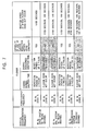
- Fig. 7 summarizes the foregoing.
- case 1 in which the vertical synchronization frequency is 60 Hz and the power-supply frequency is 50 Hz
- case 2 in which the vertical synchronization frequency is 50 Hz and the power-supply frequency is 60 Hz
- case 3 in which the vertical synchronization frequency is 60 Hz and the power-supply frequency is 60 Hz
- case 4 in which the vertical synchronization frequency is 50 Hz and the power-supply frequency is 50 Hz, are as described above.
- Fig. 7 also shows a case in which the vertical synchronization frequency (the frame frequency in this case) is 30 Hz in the CMOS imaging apparatus of the progressive system.
- the shutter when the shutter is set to a high-speed shutter with an exposure time of 1/100 seconds, 1/50 seconds, or 3/100 seconds, which is an integral multiple of the period of the luminance change of the fluorescent lamp, the amount of exposure becomes constant regardless of the exposure timing, and flicker, including in-plane flicker, does not occur.
- the shutter when the shutter is set to a high-speed shutter with an exposure time of 1/120 seconds, 1/60 seconds, or 1/40 seconds, which is an integral multiple of the period of the luminance change of the fluorescent lamp, similarly to that during the normal shutter time with an exposure time of 1/30 seconds, the amount of exposure becomes constant regardless of the exposure timing, and flicker, including in-plane flicker, does not occur.
- the shutter speed (exposure time) of the high-speed shutter may be set to a speed at which flicker does not occur, that is, 1/120 seconds in case 4; 1/100 seconds in case 3; and 1/120 seconds, 1/60 seconds, or 1/40 seconds in case 6.
- the shutter may be set to a normal shutter in which flicker does not occur. That is, in case 3, the shutter speed may be set to 1/60 seconds; in case 4, the shutter speed may be set to 1/50 seconds; and in case 6, the shutter speed may be set to 1/30 seconds.
- a method for detecting the power-supply frequency on the basis of the relationship between the period (wavelength) of a stripe pattern of the flicker and the vertical period (the reciprocal of the vertical synchronization frequency) of the imaging apparatus has been considered.
- flicker that is not continuous in the time axis and that completes in one vertical period (one picture plane) occurs in the manner described above, since a distinction between picture pattern components and fluorescent lamp flicker components in the video signal from the imaging device cannot be made from the very beginning, it is not possible to detect the power-supply frequency.
- camera shake is detected by a camera shake sensor incorporated in the camera or by a motion vector which occurs in the image, and an area of an appropriate size at an appropriate position is cut out and output from the input image on the basis of the detected amount of camera shake, thereby correcting the image signal so that the output image is always seen as being stationary.
- the shutter be set to a high-speed shutter so as to decrease the exposure time.
- the shutter speed is made too high, rough movement of the moving picture becomes conspicuous, and therefore, the shutter is set to a shutter speed with approximately 1/100 seconds at which the relationship of the above becomes just satisfactory.
- the imaging apparatus having an electronic camera-shake correction function is set so that a high-speed shutter is realized automatically when camera-shake correction is ON. That is, in order to perform electronic camera-shake correction, a high-speed shutter is necessary, and in order to solve the problem of the fluorescent-lamp flicker, the high-speed shutter cannot be omitted.
- Embodiments of the present invention relate to imaging apparatus, such as video cameras, or digital still cameras, in which an XY address scanning-type imaging device (imager, image sensor) such as a CMOS (Complementary Metal Oxide Semiconductor) imaging device is used, and to methods for reducing fluorescent lamp flicker which occurs in video signals, obtained from the imaging devices when a subject is photographed by the imaging apparatus under the illumination of a fluorescent lamp.
- an XY address scanning-type imaging device imager, image sensor
- CMOS Complementary Metal Oxide Semiconductor
- Embodiments of the present invention can reduce fluorescent-lamp flicker components regardless of the combination of the power-supply frequency and the vertical synchronization frequency of the imaging apparatus without detecting the frequency of the power supply for driving the fluorescent lamp and can realize a high-speed shutter required for electronic camera-shake correction.
- the present invention provides an imaging apparatus including an XY address scanning-type imaging device and a controller for controlling the electronic shutter speed, wherein, when the set vertical synchronization frequency of the imaging apparatus is denoted as fv (Hz) and N is a positive integer, in a case where 120/fv is an integer, the controller sets the electronic shutter speed to an electronic shutter speed at which the exposure time becomes N/120 seconds, and in a case where 100/fv is an integer, the controller sets the electronic shutter speed to an electronic shutter speed at which the exposure time becomes N/100 seconds.
- the present invention provides a method for reducing fluorescent-lamp flicker components contained in a video signal obtained by photographing a subject by an XY address scanning-type imaging device under the illumination of a fluorescent lamp, the method including, when the set vertical synchronization frequency of the imaging apparatus including the imaging device is denoted as fv (Hz) and N is a positive integer: a shutter control step of setting a shutter speed to an electronic shutter speed at which the exposure time becomes N/120 seconds in a case where 120/fv is an integer, and of setting the shutter speed to an electronic shutter speed at which the exposure time becomes N/100 seconds in a case where 100/fv is an integer; and a flicker reduction process step of reducing flicker components by estimating flicker components from the video signal and by correcting the video signal in accordance with the estimated result in a state in which the electronic shutter speed is set in the shutter control step.
- the shutter when 120/fv becomes an integer, as in the above-described case 1, case 3, case 5, or case 6, the shutter is set to a shutter speed of N/120 (seconds) in the range at which the exposure time does not exceed the vertical period 1/fv (seconds), and when 100/fv becomes an integer, as in the above-described case 2 or case 4, the shutter is set to a shutter speed of N/100 (seconds) in the range where the exposure time does not exceed the vertical period 1/fv (seconds).
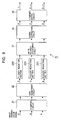
- CMOS imaging device 12 In the imaging apparatus of this embodiment, that is, the video camera, light from a subject enters a CMOS imaging device 12 via an imaging optical system 11. The light is photoelectrically converted at the CMOS imaging device 12, and an analog video signal is obtained from the CMOS imaging device 12.
- the CMOS imaging device 12 is formed in such a manner that a plurality of pixels having a photodiode (photogate), a transfer gate (shutter transistor), a switching transistor (address transistor), an amplifier transistor, a resetting transistor (reset gate), etc., are arranged two-dimensionally on a CMOS substrate, and also, a vertical scanning circuit, a horizontal scanning circuit, and a video signal output circuit are formed.
- the CMOS imaging device 12 may be of either a primary-color system or a complementary-color system, as will be described later, and the analog video signal obtained from the CMOS imaging device 12 is a primary-color signal of each RGB color, or a color signal of the complementary-color system.
- the analog video signal from the CMOS imaging device 12 is sampled and held for each color signal at an analog signal processing section 13 formed as an IC (Integrated Circuit), gain is controlled by AGC (Automatic Gain Control), and the analog video signal is converted into a digital signal by A/D conversion.
- an analog signal processing section 13 formed as an IC (Integrated Circuit)
- gain is controlled by AGC (Automatic Gain Control)
- A/D conversion Automatic Gain Control
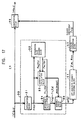
- the digital video signal from the analog signal processing section 13 is processed, as will be described later, at a digital signal processing section 20 formed as an IC. After flicker components are reduced for each signal component, as will be described later, at a flicker reduction section 25 inside the digital signal processing section 20, the signal is finally converted into a luminance signal Y and red and blue color-difference signals R-Y and B-Y, and these signals are output from the digital signal processing section 20.
- a system controller 14 is formed of a microcomputer, etc., and controls each section of the camera.
- a lens driving control signal is supplied from the system controller 14 to a lens driving driver 15 formed by an IC, and the lens and the iris of the imaging optical system 11 are driven by the lens driving driver 15.
- timing control signal is supplied from the system controller 14 to a timing generator 16.
- Various kinds of timing signals are supplied from the timing generator 16 to the CMOS imaging device 12, whereby the CMOS imaging device 12 is driven.
- the shutter speed of the CMOS imaging device 12 is also controlled in accordance with the timing control signal from the system controller 14. Specifically, the shutter speed is set by a shutter control section 14c inside the system controller 14, as will be described later.
- the detected signal of each signal component is received by the system controller 14 from the digital signal processing section 20.
- the gain of each color signal is controlled, as described above, at the analog signal processing section 13, and also, the system controller 14 controls signal processing in the digital signal processing section 20.
- a camera-shake sensor 17 is connected to the system controller 14, so that camera-shake information obtained therefrom is used for camera-shake correction.
- An operation section 18a and a display section 18b, which constitute a user interface 18, is connected via an interface 19 formed by a microcomputer, etc., to the system controller 14.
- the setting operation and the selection operation at the operation section 18a are detected by the system controller 14, and also, the set status and the control status of the camera are displayed on the display section 18b by the system controller 14.
- the set status of one of the NTSC system and the PAL system described above is held as a setting flag inside the system controller 14, so that it is used for shutter control (to be described later) by the shutter control section 14c.
- Fig. 9 shows an example of a digital signal processing section 20 in the case of a primary-color system.
- the primary-color system has a color separation optical system in which the imaging optical system 11 of Fig. 8 separates light from a subject into color light of each of RGB, and is a three-plate system having CMOS imaging apparatuses for each RGB color as the CMOS imaging devices 12, or a one-plate system having one CMOS imaging apparatus as the CMOS imaging device 12, in which a color filter for each RGB color is arranged repeatedly in sequence for each pixel on the light incidence plane in the horizontal direction of the picture plane.
- primary-color signals for each RGB color are read in parallel from the CMOS imaging devices 12.
- the black level of the input RGB primary-color signal is clamped to a predetermined level at the clamping circuit 21; the gain of the clamped RGB primary-color signal is adjusted according to the amount of exposure at the gain adjustment circuit 22; and flicker components in the RGB primary-color signal whose gain is adjusted is reduced by a method (to be described later) at flicker reduction sections 25R, 25G, and 25B.
- white balance of the RGB primary-color signal after flicker is reduced is adjusted at the white-balance adjustment circuit 27; the gradation of the RGB primary-color signal after white balance is adjusted is converted at the gamma correction circuit 28; and an output luminance signal Y and output color-difference signals R-Y and B-Y are generated from the gamma-corrected RGB primary-color signals at the combined matrix circuit 29.
- the flicker components in the RGB primary-color signals in the step of processing the RGB primary-color signals as shown in Fig. 9 can be sufficiently reduced.
- the flicker reduction section 25 may be provided on the output side of the luminance signal Y of the combined matrix circuit 29, so that flicker components in the luminance signal Y are detected and reduced.
- the complementary-color system is a one-plate system having one CMOS imaging device as the CMOS imaging device 12 of Fig. 8, in which a color filter of the complementary-color system is formed on the light incidence plane.
- the complementary-color system video signals at two adjacent horizontal line positions are combined and read from the CMOS imaging device 12; in the digital signal processing section 20, the black level of the complementary-color signal (combined signal) is clamped to a predetermined level, the gain of the clamped complementary-color signal is adjusted according to the amount of exposure, and a luminance signal and RGB primary-color signals are generated from the gain-adjusted complementary-color signal.
- the flicker reduction section 25 the flicker components in the luminance signal and the flicker components in the RGB primary-color signals are reduced, and the gradation of the luminance signal after flicker is reduced is corrected, obtaining the output luminance signal Y. Also, white balance of the RGB primary-color signal after flicker is adjusted, the gradation of the RGB primary-color signal after white balance is adjusted is converted, and color-difference signals R-Y and B-Y are generated from the RGB primary-color signals after gamma correction.
- the shutter is controlled and the shutter speed is set by the method described below.
- the shutter control section 14c of the system controller 14 performs a shutter control process described below for each field so that the shutter speed is set.
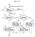
- Figs. 10 to 12 show an example of a shutter control process routine performed by the shutter control section 14c.
- a shutter control process routine 100 of this example initially, in step 101, it is determined whether or not the photographic environment is indoors.
- the brightness information of AE (Auto Exposure) control, the color temperature information of white balance control, etc., used for normal camera control, can be used.
- step 101 normal shutter control is performed, that is, an electronic shutter is set in the normal exposure control mode, completing the shutter control process.
- step 101 the process proceeds from step 101 to step 103, where it is determined whether or not the fluorescent-lamp illumination detection mode is ON.
- the on/off state of the fluorescent-lamp illumination detection mode is set by the system controller 14 itself, and is controlled in such a manner that, when the imaging apparatus is powered on or when the subject information (the brightness and the color temperature of the subject) is greatly changed, the detection mode is turned on, and the detection mode is turned off in a steady state.
- step 103 when the fluorescent-lamp illumination detection mode is ON, the process proceeds from step 103 to step 104, where detection mode processing is performed. Thereafter, the process proceeds to step 105, where it is determined whether or not the photographic environment is under the illumination of a fluorescent lamp on the basis of the processing result.
- the video signal (each color signal or the luminance signal) obtained at the digital signal processing section 20 is integrated in the horizontal direction of the picture plane, obtaining an integrated value for each field (the waveform of Fig. 13B shows flicker components), and as shown in Fig. 13C, the difference (Fn - Fn_1) of the integrated value between adjacent fields is computed.
- the system controller 14 drives the imaging apparatus by slightly disrupting the constantness of the vertical period only during the detection mode.
- the vertical period the time from a particular vertical synchronization signal VD to the next vertical synchronization signal VD is alternately increased or decreased by ⁇ (seconds) every vertical period.
- case 1 the constantness of the vertical period is slightly disrupted in this manner regardless of whether the set vertical synchronization frequency fv of the imaging apparatus is 60 Hz or 50 Hz and without detecting whether the power-supply frequency fp is 50 Hz or 60 Hz.
- the circuit block used in that flicker reduction method can also be used for integration and difference computations shown in Figs. 13A, 13B, and 13C.
- step 103 When it is determined in step 103 that the fluorescent-lamp illumination detection mode is in a steady state of OFF, the process proceeds to step 106, where the processing results (determination results) in the previous or past detection mode are received, and the process then proceeds to step 105.
- step 105 when it is determined in step 105 that the photographic environment is not under the illumination of a fluorescent lamp, since the flicker reduction process is not necessary from the beginning, similarly to the case of outdoor photographing, the process proceeds to step 102, where normal shutter control is performed, completing the shutter control process.
- step 105 when it is determined in step 105 that the photographic environment is under the illumination of a fluorescent lamp, the process proceeds to step 107, where it is determined whether or not camera-shake correction is ON.
- step 111 it is determined whether the set vertical synchronization frequency fv is 60 Hz or 50 Hz on the basis of the above-described setting flag, and the shutter is set to a high-speed shutter of a shutter speed corresponding to the determination result.
- the shutter when camera-shake correction is ON, the shutter may always be set to a high-speed shutter.
- the shutter when the luminance (brightness) of the subject is very low (dark) and the optimum exposure takes precedence over the improvement of the image quality by the high-speed shutter when the camera-shake correction is performed, the shutter may be set exceptionally to a normal shutter.
- the following example shows a case in which the shutter is set to a high-speed shutter in principle and is set exceptionally to a normal shutter when the camera-shake correction is ON in this manner.
- fv 50 Hz as in case 2 or case 4
- the shutter is set to a high-speed shutter with a shutter speed of 1/100 seconds when camera-shake correction is ON.
- the shutter control section 14c need only make a determination as to whether the set video system is the NTSC system or the PAL system (as to whether the vertical synchronization frequency fv is 60 Hz or 50 Hz). Furthermore, when the camera-shake correction is ON, a high-speed shutter can be realized in principle, and the improvement in image quality by the high-speed shutter can be achieved.
- step 113 After the shutter speed is set in step 113, 114, 116, or 117, the process proceeds to step 118, where iris adjustment and AGC are performed in accordance with the set shutter speed so that the optimum exposure is achieved along with the setting of the shutter speed, completing the shutter control process.
- the difference is approximately 0.8 dB, which can be sufficiently compensated for by iris adjustment and AGC in step 108, and the image quality does not deteriorate due to a decrease in the amount of exposure. Moreover, in the case of the shutter speed of 1/120 seconds, the rough movement of the moving image does not become conspicuous.
- step 107 when camera-shake correction is OFF, that is, when camera shake correction is not to be performed, the process proceeds from step 107 to step 121, where it is determined whether the set vertical synchronization frequency fv is 60 Hz or 50 Hz on the basis of the above-described setting flag, and the shutter is set to a normal shutter with a shutter speed corresponding to the determination result.
- the shutter when camera-shake correction is OFF, the shutter may be always set to a normal shutter for optimum exposure, but when the luminance (brightness) of the subject is very high (bright), the shutter may be exceptionally set to a high-speed shutter.
- the following example shows a case in which the shutter is set to a normal shutter in principle and is set exceptionally to a high-speed shutter when the camera-shake correction is OFF in this manner.
- step 108 iris adjustment and AGC are performed in accordance with the set shutter speed so that the optimum exposure is achieved along with the setting of the shutter speed, completing the shutter control process.
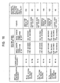
- the above shutter control process is shown in the column in which the vertical synchronization frequency is 60 Hz or 50 Hz in Fig. 16.
- the shutter speeds indicated within the parentheses when the camera-shake correction is ON and the camera-shake correction is OFF are exceptional shutter speeds set in steps 114, 117, 124, and 127.
- the shutter speeds indicated outside the parentheses thereabove are shutter speeds, which are set in principle in steps 113, 116, 123, and 126.
- the shutter control of the present invention can also be applied to a case in which the vertical synchronization frequency (the frame frequency in this case) fv is, for example, 30 Hz, in a CMOS imaging apparatus of the progressive system, such as a digital still camera.
- the imaging apparatus in this case is also configured basically as shown in Fig. 8.
- the shutter control section 14c of the system controller 14 performs a shutter control process described below for each frame and sets the shutter speed.
- Fig. 15 shows an example of a shutter control process routine performed by the shutter control section 14c.
- the steps from the start of the shutter control process up to step 107 are the same as the steps from the start of the shutter control process of the shutter control process routine 100 up to step 107.
- step 107 when the photographic environment is under the illumination of a fluorescent lamp, it is determined in step 107 whether or not camera-shake correction is ON.
- camera-shake correction is ON, that is, when camera-shake correction is to be performed, the shutter is set to a high-speed shutter.
- camera-shake correction is OFF, that is, when camera-shake correction is not to be performed, the shutter is set to a normal shutter.
- the shutter may be always set to a high-speed shutter when camera-shake correction is ON, and the shutter may be always set to a normal shutter when camera-shake correction is OFF.
- the following example shows a case in which the shutter is set to a high-speed shutter in principle and is set exceptionally to a normal shutter when the camera-shake correction is ON, and the shutter is set to a normal shutter in principle and is set exceptionally to a high-speed shutter when the camera-shake correction is OFF.
- the shutter speed is set to 1/120 seconds. Furthermore, in a case where the shutter speed is subdivided according to the luminance of the subject, when the luminance of the subject is a predetermined value V1 (> V2) or higher in the range where the luminance is greater than or equal to the threshold value V2, the shutter speed is set to 1/120 seconds. When the luminance of the subject is less than the predetermined value V1 in the range where the luminance is greater than or equal to the threshold value V2, the shutter speed is set to 1/60 seconds.
- the shutter speed is set to 1/30 seconds. Furthermore, in a case where the shutter speed is subdivided according to the luminance of the subject, when the luminance of the subject is less than a predetermined value V3 ( ⁇ V2) in the range where the luminance is less than the threshold value V2, the shutter speed is set to 1/30 seconds. When the luminance of the subject is greater than or equal to the predetermined value V3 in the range where the luminance is less than the threshold value V2, the shutter speed is set to 1/40 seconds.
- step 107 when it is determined in step 107 that the camera-shake correction is OFF, the process proceeds to step 135, where it is determined whether or not the luminance of the subject is higher than a threshold value V4.
- step 133 After the shutter speed is set in step 133, 134, 136, or 137, the process proceeds to step 108, where iris adjustment and AGC are performed, completing the shutter control process.
- the above shutter control process is shown in the column in which the vertical synchronization frequency is 30 Hz in Fig. 16.
- the shutter speed is set to 1/120 seconds, 1/60 seconds, 1/40 seconds, or 1/30 seconds
- flicker having continuity in a time axis that is, flicker whose repetition period is three frames, occurs, and thus flicker components can be reduced by the flicker reduction method using the continuity of flicker.
- flicker does not occur to begin with, and the flicker reduction process is not necessary.
- the flicker reduction process is further performed by the flicker reduction section 25 inside the digital signal processing section 20 under the control of the system controller 14.
- any method may be used as long as it is a method in which flicker components are reduced by estimating flicker components using the continuity of flicker from the video signal from the imaging device and by correcting the video signal from the imaging apparatus according to the estimated result in the manner described above.
- flicker reduction method of the invention of the earlier application Japanese Patent Application No. 2003-173642
- flicker components specific to an XY address scanning-type imaging device such as a CMOS imaging device can be detected with high accuracy, and can be reduced reliably and sufficiently by simple signal processing regardless of the subject, the video signal level, and the type of fluorescent lamp.
- the flicker reduction method of the invention of the earlier application includes (a) a step of using a video signal from an imaging apparatus and integrating the input image signal over the time of one horizontal period or more; (b) a step of normalizing the integration value, or the difference value of the integration values in adjacent fields or frames; (c) a step of extracting the spectrum of the normalized integration value or the normalized difference value; (d) a step of estimating flicker components from the extracted spectrum; and (e) a step of computing the estimated flicker components and the input image signal so as to cancel out the estimated flicker components.
- the difference value is divided by the average value of the integrated values in a plurality of continuous fields or in a plurality of continuous frames, or (b2) the integrated value is divided by the average value of the integrated values in the plurality of continuous fields or in the plurality of continuous frames, and a predetermined value is subtracted from the division result, or (b3) the difference value is divided by the integrated value.
- the spectrum extraction step (c) a method of performing a Fourier transform on the normalized integrated value or the difference value is used.
- the flicker reduction sections 25R, 25G, and 25B for the RGB primary-color signals of the primary-color system shown in Fig. 9 and the flicker reduction section 25 for the RGB primary-color signals and the luminance signal of the complementary-color system are configured, for example, as shown as the flicker reduction section 25 in Fig. 17.
- flicker having continuity in a time axis that is, flicker whose repetition period is three fields
- the input image signal is the RGB primary-color signals or the luminance signal before the flicker reduction process is performed thereon, which is input to the flicker reduction section 25
- the output image signal is the RGB primary-color signal or the luminance signal after the flicker reduction process is performed thereon, which is output from the flicker reduction section 25.
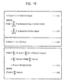
- Figs. 3 and 4 show a case in which the subject is uniform. In general, flicker components are proportional to the signal intensity of the subject.
- In' (x, y) is represented as the sum of the signal components which do not contain flicker components and flicker components proportional thereto on the basis of equation (1) of Fig. 18.
- In (x, y) indicates signal components
- ⁇ n (y) * In (x, y) indicates flicker components
- ⁇ n (y) indicates a flicker coefficient.
- the flicker coefficient is denoted as ⁇ n (y).
- the flicker coefficient is described in a form in which the flicker coefficient is expanded to a Fourier series.
- the flicker coefficient can be represented in a form in which light-emitting characteristics and persistence characteristics, which differ depending on the type of fluorescent lamp, are all covered.
- ⁇ mn indicates the initial phase of the flicker components of each order, which is determined by the light-emitting period of the fluorescent lamp and the exposure timing.
- fv 60 Hz
- ⁇ mn becomes the same value every three fields, the difference of ⁇ mn with the previous field is represented by equation (3) of Fig. 18.
- the input image signal In' (x, y) is integrated over one line in the horizontal direction of the picture plane by the integration block 31, thus computing the integrated value Fn (y) as indicated in equation (4) of Fig. 18.
- ⁇ n (y) in equation (4) indicates an integrated value over one line of the signal components In (x, y), as indicated in equation (5) of Fig. 18.
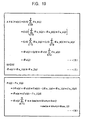
- the computed integrated value Fn (y) is stored and held in the integration-value holding block 32 for the purpose of detecting flicker in subsequent fields.
- the integration-value holding block 32 is configured so as to hold integrated values for at least two fields.
- an integrated value Fn_1 (y) of the same line one field before and an integrated value Fn_2 (y) of the same line two fields before are read from the integration-value holding block 32, and an average value AVE [Fn (y)] of the three integrated values Fn (y), Fn_1 (y), and Fn_2 (y) is computed at an average-value calculation block 33.
- the flicker reduction section 25 for which a case in which the motion of the subject is large is assumed need only hold the integrated values over the three or more fields in the integration-value holding block 32 so as to compute the average value of the integrated values over the four or more fields together with the integrated value Fn (y) of the corresponding field.
- the low-pass filter action in the direction of the time axis causes the influence as a result of the subject being moved to be decreased.
- the integration-value holding block 32 is configured to hold integrated values for at least (j - 1) fields.
- Fig. 17 shows a case in which the approximation of equation (7) of Fig. 19 holds.
- a difference calculation block 34 calculates the difference between the integrated value Fn (y) of the corresponding field from the integration block 31 and the integrated value Fn_1 (y) one field before from the integration-value holding block 32, and the difference value Fn (y) - Fn_1 (y) represented by equation (8) of Fig. 19 is computed.
- Equation (8) also presupposes that the approximation of equation (7) holds.
- the difference value Fn (y) - Fn_1 (y) from the difference calculation block 34 is normalized as a result of being divided by the average value AVE [Fn (y)] from the average-value calculation block 33, and a difference value gn (y) after normalization is computed.
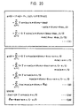
- a discrete Fourier transform is performed on data corresponding to the amount of one wavelength (the amount of L lines) of flicker, of the difference value gn (y) after normalization from the normalization block 35.
- equation (13) the DFT computation is represented by equation (13) of Fig. 21.
- W in equation (13) is represented by equation (14).
- equations (15a) and (15b) of Fig. 21 the relationships between equations (11a) and (11b) and equation (13) are represented by equations (15a) and (15b) of Fig. 21.
- FFT Fast Fourier Transform
- the spectrum is extracted by the DFT computation defined by equation (13), and thereafter, the amplitude ym and the initial phase ⁇ mn of the flicker components of each order are estimated by the computations of equations (16a) and (16b).
- a flicker coefficient ⁇ n (y) represented by equation (2) of Fig. 18 is computed from the estimated values of ⁇ m and ⁇ mn from the DFT block 51.
- the sum order can be limited to a predetermined order, for example, a second order rather than being set to infinity.
- the difference value Fn (y) - Fn_1 (y) is computed, and this is normalized by the average value AVE [Fn (y)], making it possible to detect the flicker components with high accuracy.
- the estimation of the flicker components from the spectrum up to an appropriate order results in the approximation without completely reproducing the difference value gn (y) after normalization.
- the difference value gn (y) after normalization depends on the status of the subject, it is possible to estimate the flicker components of that portion with high accuracy.
- a function for holding the flicker coefficient ⁇ n (y) over three fields may be provided within the computation block 40, so that the held flicker coefficient ⁇ n (y) is computed on the input image signal In' (x, y) after three fields.
- Fig. 17 shows a case in which the difference value Fn (y) - Fn_1 (y), rather than the integrated value Fn (y) like another configuration example (to be described later), is normalized by the average value AVE [Fn (y)].
- the front-stage part of the DFT block 51 in the flicker reduction section 25 is referred to as a "normalized integrated-value computation block 30".
- the difference value Fn (y) - Fn_1 (y) is normalized by the average value AVE [Fn (y)] as in the example of Fig. 17, a finite calculation accuracy can be ensured effectively.
- the integrated value Fn (y) from the integration block 31 may be directly normalized by the average value AVE [Fn (y)].
- the amplitude ⁇ m and the initial phase ⁇ mn of the flicker components of each order are estimated by the computations of equations (16a) and (16b).
- the amplitude ⁇ m and the initial phase ⁇ mn of the flicker components of each order are estimated by the computations of equations (20a) and (20b).
- the subsequent processing is the same as that of the example of Fig. 17.
- the flicker reduction section 25 can be simplified correspondingly.
- the average value AVE [Fn (y)] used for the normalization of the difference value Fn (y) - Fn_1 (y) is equal to ⁇ n (y) as indicated in equation (6) when the approximation of equation (7) of Fig. 19 holds, and the second term [ ⁇ n (y) * ⁇ n (y)] of equation (4) of Fig. 18 is small sufficiently when compared to the ⁇ n (y) in the first term. Therefore, the influence of the second term on the normalization is very small.
- the integration-value holding block 32 need only hold the integrated values for one field, and since the average-value calculation block 33 is not required, the flicker reduction section 25 can be simplified.
- Each of the above-described examples shows a case in which the input image signal In' (x, y) is integrated over one line. Since the integration of the input image signal In' (x, y) is for the purpose of obtaining sampled values of the flicker components by reducing the influence of the picture pattern, the integration may be performed over the time for a plurality of lines without being limited to one line.
- the integration time may not be just an integral multiple of the horizontal period like a 2.5 horizontal period.
- the load of DFT computation on the DFT block 51 can be lessened and also, when the subject is moved in the vertical direction of the picture plane, the influence thereof can be decreased.
- a check is made to determine for each pixel whether or not the level of the input image signal In' (x, y) is higher than or equal to a threshold level of the saturation area.
- the computation result of equation (17) is output as the output image signal In (x, y) in the manner described above.
- the input image signal In' (x, y) is output as is as the output image signal In (x, y).
- the signal components (the color components or the luminance components) do not change, and thus an output image signal with high image quality can be obtained.
- the exposure timings (the exposure start timing and the exposure end timing) of all the pixels within one picture plane can be made the same, and the occurrence of fluorescent-lamp flicker can be avoided, making the flicker reduction process unnecessary.
- reading of a video signal from the CMOS imaging device can be performed slowly in a state in which light is shielded with the mechanical shutter being closed because there is no limitation of the electronic shutter speed as in the case of photographing a moving image.
- the flicker reduction section 25 is controlled by the system controller 14 so that the flicker reduction process is not performed in the flicker reduction section 25, and the input image signal In' (x, y) is output as is as the output image signal In (x, y).
- the flicker reduction section 25 may be configured so as to deal with the flicker ("three fields" in the case of the NTSC system is replaced with "five fields").
- the flicker reduction section 25 may be configured in such a manner that the flicker reduction section 25 is also switched for use with the NTSC system, and when the camera is set to the PAL system, the flicker reduction section 25 is also switched for use with the PAL system.
- the flicker reduction section 25 may be configured so as to deal with the flicker ("fields" in the case of the NTSC system is replaced with "frames", that is, "three fields” is replaced with "three frames”).
- the present invention can be applied when the vertical synchronization frequency fv is not 30 Hz, but, for example, 40 Hz or 25 Hz.
- the above-described embodiment shows a case in which the digital signal processing section 20 including the flicker reduction section 25 is formed by hardware.
- a part or the entirety of the flicker reduction section 25 or the digital signal processing section 20 may be formed by software.
- the present invention can also be applied to an imaging apparatus using an XY address scanning-type imaging device other than a CMOS imaging device.
- fluorescent-lamp flicker components can be reduced regardless of the combination of the power-supply frequency and the vertical synchronization frequency of the imaging apparatus without detecting the frequency of the power supply for driving the fluorescent lamp, and also, a high-speed shutter required for electronic camera-shake correction can be realized.
Landscapes
- Engineering & Computer Science (AREA)
- Multimedia (AREA)
- Signal Processing (AREA)
- Studio Devices (AREA)
- Transforming Light Signals Into Electric Signals (AREA)
- Picture Signal Circuits (AREA)
Applications Claiming Priority (2)
| Application Number | Priority Date | Filing Date | Title |
|---|---|---|---|
| JP2003272015A JP3826904B2 (ja) | 2003-07-08 | 2003-07-08 | 撮像装置およびフリッカ低減方法 |
| JP2003272015 | 2003-07-08 |
Publications (2)
| Publication Number | Publication Date |
|---|---|
| EP1496690A2 true EP1496690A2 (de) | 2005-01-12 |
| EP1496690A3 EP1496690A3 (de) | 2005-02-09 |
Family
ID=33448045
Family Applications (1)
| Application Number | Title | Priority Date | Filing Date |
|---|---|---|---|
| EP04254041A Ceased EP1496690A3 (de) | 2003-07-08 | 2004-07-06 | Bildgeber und Flimmerreduktionsverfahren |
Country Status (6)
| Country | Link |
|---|---|
| US (1) | US7705893B2 (de) |
| EP (1) | EP1496690A3 (de) |
| JP (1) | JP3826904B2 (de) |
| KR (1) | KR101007427B1 (de) |
| CN (1) | CN100423555C (de) |
| TW (1) | TWI239212B (de) |
Cited By (14)
| Publication number | Priority date | Publication date | Assignee | Title |
|---|---|---|---|---|
| EP1732313A1 (de) * | 2005-06-10 | 2006-12-13 | Sony Corporation | Bildverarbeitungsvorrichtung und Bildaufnahmevorrichtung |
| EP1734747A1 (de) * | 2005-06-13 | 2006-12-20 | Sony Corporation | Bildverarbeitungsvorrichtung und Bildaufnahmevorrichtung |
| CN100337471C (zh) * | 2005-10-21 | 2007-09-12 | 北京中星微电子有限公司 | 一种行曝光模式下闪烁的简单判断和消除方法 |
| EP1758374A3 (de) * | 2005-08-26 | 2011-05-18 | Sony Corporation | Vorrichtung und Verfahren zur Belichtungskontrolle und Bildaufnahmevorrichtung |
| CN1882047B (zh) * | 2005-06-13 | 2011-06-15 | 索尼株式会社 | 图像处理设备和图像拾取设备 |
| EP1763228A3 (de) * | 2005-09-08 | 2011-06-22 | Sony Corporation | Flimmerreduktionverfahren, -schaltung und Bildaufnahmevorrichtung |
| CN102223486A (zh) * | 2011-04-13 | 2011-10-19 | 北京瑞澜联合通信技术有限公司 | 低照度摄像机成像控制方法、装置及摄像系统 |
| EP3474544A4 (de) * | 2016-06-15 | 2019-06-19 | Sony Corporation | Bildverarbeitungsvorrichtung, bildverarbeitungsverfahren und programm |
| EP3580609A4 (de) * | 2017-02-10 | 2020-11-11 | Novadaq Technologies ULC | Handhaltbare offenfeld-fluoreszenzbildgebungssysteme und verfahren |
| CN112565595A (zh) * | 2020-11-25 | 2021-03-26 | 西安闻泰电子科技有限公司 | 图像抖动消除方法、装置、电子设备和存储介质 |
| US10980420B2 (en) | 2016-01-26 | 2021-04-20 | Stryker European Operations Limited | Configurable platform |
| US11025867B2 (en) | 2006-12-22 | 2021-06-01 | Stryker European Operations Limited | Imaging systems and methods for displaying fluorescence and visible images |
| US11756674B2 (en) | 2016-06-14 | 2023-09-12 | Stryker European Operations Limited | Methods and systems for adaptive imaging for low light signal enhancement in medical visualization |
| US11930278B2 (en) | 2015-11-13 | 2024-03-12 | Stryker Corporation | Systems and methods for illumination and imaging of a target |
Families Citing this family (70)
| Publication number | Priority date | Publication date | Assignee | Title |
|---|---|---|---|---|
| US8471852B1 (en) | 2003-05-30 | 2013-06-25 | Nvidia Corporation | Method and system for tessellation of subdivision surfaces |
| JP3826904B2 (ja) * | 2003-07-08 | 2006-09-27 | ソニー株式会社 | 撮像装置およびフリッカ低減方法 |
| CN100484197C (zh) * | 2004-11-15 | 2009-04-29 | 索尼株式会社 | 闪烁校正方法、闪烁校正电路、以及使用它们的摄像装置 |
| US7538799B2 (en) * | 2005-01-14 | 2009-05-26 | Freescale Semiconductor, Inc. | System and method for flicker detection in digital imaging |
| JP2006243381A (ja) * | 2005-03-03 | 2006-09-14 | Fuji Photo Film Co Ltd | 撮影装置 |
| US7683948B2 (en) * | 2005-03-31 | 2010-03-23 | Freescale Semiconductor, Inc. | System and method for bad pixel replacement in image processing |
| JP2006287362A (ja) * | 2005-03-31 | 2006-10-19 | Eastman Kodak Co | デジタルカメラおよびホワイトバランス調整方法 |
| JP4377840B2 (ja) * | 2005-03-31 | 2009-12-02 | イーストマン コダック カンパニー | デジタルカメラ |
| JP4207923B2 (ja) * | 2005-04-19 | 2009-01-14 | ソニー株式会社 | フリッカ補正方法、フリッカ補正装置及び撮像装置 |
| JP2006310974A (ja) * | 2005-04-26 | 2006-11-09 | Mitsubishi Electric Corp | 撮像装置 |
| JP4539432B2 (ja) * | 2005-05-16 | 2010-09-08 | ソニー株式会社 | 画像処理装置および撮像装置 |
| US7710458B2 (en) * | 2005-06-17 | 2010-05-04 | Casio Computer Co., Ltd. | Image pick-up apparatus with a shake reducing function |
| JP2007019973A (ja) * | 2005-07-08 | 2007-01-25 | Fujifilm Holdings Corp | 撮像装置及び撮像方法 |
| US7777787B2 (en) * | 2005-10-17 | 2010-08-17 | Nokia Corporation | Preventing flicker effects in video electronic devices |
| US8571346B2 (en) | 2005-10-26 | 2013-10-29 | Nvidia Corporation | Methods and devices for defective pixel detection |
| US7750956B2 (en) | 2005-11-09 | 2010-07-06 | Nvidia Corporation | Using a graphics processing unit to correct video and audio data |
| US7598987B2 (en) * | 2005-11-29 | 2009-10-06 | Stmicroelectronics Asia Pacific Pte. Ltd. | Flicker detection gain control circuit, digital imaging system, and method |
| US8588542B1 (en) | 2005-12-13 | 2013-11-19 | Nvidia Corporation | Configurable and compact pixel processing apparatus |
| US8737832B1 (en) | 2006-02-10 | 2014-05-27 | Nvidia Corporation | Flicker band automated detection system and method |
| JP2007336470A (ja) * | 2006-06-19 | 2007-12-27 | Sony Corp | 撮像装置及び撮像方法 |
| JP4948090B2 (ja) * | 2006-08-25 | 2012-06-06 | キヤノン株式会社 | 撮像装置及び駆動制御方法 |
| US8594441B1 (en) | 2006-09-12 | 2013-11-26 | Nvidia Corporation | Compressing image-based data using luminance |
| US8723969B2 (en) | 2007-03-20 | 2014-05-13 | Nvidia Corporation | Compensating for undesirable camera shakes during video capture |
| TWI366391B (en) * | 2007-06-28 | 2012-06-11 | Novatek Microelectronics Corp | Method and circuit for correcting signals and image correcting method and circuit using the same |
| US8724895B2 (en) | 2007-07-23 | 2014-05-13 | Nvidia Corporation | Techniques for reducing color artifacts in digital images |
| US8570634B2 (en) | 2007-10-11 | 2013-10-29 | Nvidia Corporation | Image processing of an incoming light field using a spatial light modulator |
| US9177368B2 (en) | 2007-12-17 | 2015-11-03 | Nvidia Corporation | Image distortion correction |
| US8780128B2 (en) | 2007-12-17 | 2014-07-15 | Nvidia Corporation | Contiguously packed data |
| US8217887B2 (en) * | 2008-01-23 | 2012-07-10 | Atmel Corporation | System and method for backlight control for an electronic display |
| US8698908B2 (en) | 2008-02-11 | 2014-04-15 | Nvidia Corporation | Efficient method for reducing noise and blur in a composite still image from a rolling shutter camera |
| US9379156B2 (en) | 2008-04-10 | 2016-06-28 | Nvidia Corporation | Per-channel image intensity correction |
| CN101582992B (zh) * | 2008-05-15 | 2012-12-19 | 鸿富锦精密工业(深圳)有限公司 | 闪烁消除系统及消除闪烁的方法 |
| JP5188275B2 (ja) | 2008-06-06 | 2013-04-24 | キヤノン株式会社 | 固体撮像装置、その駆動方法及び撮像システム |
| JP4907611B2 (ja) * | 2008-07-29 | 2012-04-04 | 京セラ株式会社 | 撮像装置、フリッカー抑制方法、及びフリッカー抑制プログラム |
| US7911505B2 (en) * | 2008-08-20 | 2011-03-22 | Eastman Kodak Company | Detecting illuminant flicker |
| US8194152B2 (en) * | 2008-09-05 | 2012-06-05 | CSR Technology, Inc. | Image processing under flickering lighting conditions using estimated illumination parameters |
| US8373718B2 (en) | 2008-12-10 | 2013-02-12 | Nvidia Corporation | Method and system for color enhancement with color volume adjustment and variable shift along luminance axis |
| KR20100091845A (ko) * | 2009-02-11 | 2010-08-19 | 삼성전자주식회사 | 플리커 발생을 방지하는 디지털 촬영 장치, 이의 제어 방법및 상기 제어 방법을 기록한 기록 매체 |
| US8749662B2 (en) | 2009-04-16 | 2014-06-10 | Nvidia Corporation | System and method for lens shading image correction |
| JP5460180B2 (ja) * | 2009-08-25 | 2014-04-02 | キヤノン株式会社 | 撮像装置及びその制御方法 |
| US8698918B2 (en) | 2009-10-27 | 2014-04-15 | Nvidia Corporation | Automatic white balancing for photography |
| US8624999B2 (en) * | 2009-12-01 | 2014-01-07 | Ricoh Company, Ltd. | Imaging apparatus |
| US8462229B2 (en) * | 2010-09-30 | 2013-06-11 | Hewlett-Packard Development Company, L.P. | Detection of flicker within captured imaged frames |
| CN102025920B (zh) * | 2010-11-17 | 2012-08-29 | 无锡中星微电子有限公司 | 曝光时间调整方法和装置以及应用此装置的摄像头 |
| US8836772B2 (en) * | 2010-11-17 | 2014-09-16 | Sony Computer Entertainment, Inc. | 3D shutter glasses with frame rate detector |
| JP5343995B2 (ja) * | 2010-11-25 | 2013-11-13 | カシオ計算機株式会社 | 撮像装置、撮像制御方法及びプログラム |
| US9418270B2 (en) | 2011-01-31 | 2016-08-16 | Hand Held Products, Inc. | Terminal with flicker-corrected aimer and alternating illumination |
| CN102427509A (zh) * | 2011-09-16 | 2012-04-25 | 杭州海康威视数字技术股份有限公司 | 一种控制补光灯同步摄像机的装置及方法 |
| TWI469632B (zh) * | 2011-11-09 | 2015-01-11 | Silicon Motion Inc | 抗閃爍攝錄裝置與攝錄方法 |
| CN103220476B (zh) * | 2012-01-20 | 2016-03-16 | 联咏科技股份有限公司 | 图像处理装置及方法 |
| KR101357404B1 (ko) * | 2012-05-08 | 2014-02-12 | (주) 넥스트칩 | 다중 노출 영상 분석을 이용하여 색상 보정 및 플리커 제거를 수행하는 시스템 및 방법 |
| US9798698B2 (en) | 2012-08-13 | 2017-10-24 | Nvidia Corporation | System and method for multi-color dilu preconditioner |
| US9508318B2 (en) | 2012-09-13 | 2016-11-29 | Nvidia Corporation | Dynamic color profile management for electronic devices |
| US9307213B2 (en) | 2012-11-05 | 2016-04-05 | Nvidia Corporation | Robust selection and weighting for gray patch automatic white balancing |
| WO2014167865A1 (ja) * | 2013-04-12 | 2014-10-16 | パナソニック インテレクチュアル プロパティ コーポレーション オブ アメリカ | フリッカ低減装置、撮像装置およびフリッカ低減方法 |
| CN103327239A (zh) * | 2013-05-31 | 2013-09-25 | Tcl通讯(宁波)有限公司 | 一种基于移动终端的摄像头数据处理方法及移动终端 |
| JP6104060B2 (ja) * | 2013-06-06 | 2017-03-29 | オリンパス株式会社 | 撮像装置、撮像方法 |
| US9826208B2 (en) | 2013-06-26 | 2017-11-21 | Nvidia Corporation | Method and system for generating weights for use in white balancing an image |
| US9756222B2 (en) | 2013-06-26 | 2017-09-05 | Nvidia Corporation | Method and system for performing white balancing operations on captured images |
| CN104301617B (zh) | 2013-07-19 | 2017-09-22 | 富士通株式会社 | 闪烁检测方法和闪烁检测设备 |
| CN104301618B (zh) * | 2013-07-19 | 2017-11-14 | 富士通株式会社 | 闪烁检测方法和闪烁检测设备 |
| KR101591172B1 (ko) * | 2014-04-23 | 2016-02-03 | 주식회사 듀얼어퍼처인터네셔널 | 이미지 센서와 피사체 사이의 거리를 결정하는 방법 및 장치 |
| JP6175587B2 (ja) | 2015-03-02 | 2017-08-02 | 富士フイルム株式会社 | 撮像装置、フリッカ検出方法、及びフリッカ検出プログラム |
| WO2016139846A1 (ja) | 2015-03-02 | 2016-09-09 | 富士フイルム株式会社 | 撮像装置、フリッカ検出方法、及びフリッカ検出プログラム |
| CN105430290B (zh) * | 2015-11-24 | 2019-04-16 | 青岛海信移动通信技术股份有限公司 | 一种水波纹的预消除方法及拍照设备 |
| WO2017090300A1 (ja) * | 2015-11-24 | 2017-06-01 | ソニー株式会社 | 画像処理装置、および画像処理方法、ならびにプログラム |
| WO2019071543A1 (en) * | 2017-10-12 | 2019-04-18 | SZ DJI Technology Co., Ltd. | SYSTEMS AND METHODS FOR AUTOMATIC DETECTION AND CORRECTION OF LUMINANCE VARIATIONS ON IMAGES |
| CN108462837B (zh) * | 2018-03-13 | 2022-06-21 | 中兴通讯股份有限公司 | 拍摄方法及装置 |
| CN110035234A (zh) * | 2019-04-16 | 2019-07-19 | 深圳市道通智能航空技术有限公司 | 一种飞行器的拍摄控制方法、飞行器及飞行系统 |
| US20260046527A1 (en) * | 2024-08-08 | 2026-02-12 | Qualcomm Incorporated | Flicker detection and correction for image frames |
Citations (3)
| Publication number | Priority date | Publication date | Assignee | Title |
|---|---|---|---|---|
| US6157406A (en) | 1994-04-08 | 2000-12-05 | Hitachi, Ltd. | Image pickup apparatus and method of controlling the same |
| US20020154225A1 (en) | 2001-04-23 | 2002-10-24 | Hiroyuki Matsumoto | Imaging system using solid-state CMOS imaging device |
| US20030090566A1 (en) | 1998-07-28 | 2003-05-15 | Smith Ronald D. | Method and apparatus for reducing flicker effects from discharge lamps during pipelined digital video capture |
Family Cites Families (10)
| Publication number | Priority date | Publication date | Assignee | Title |
|---|---|---|---|---|
| JP2687670B2 (ja) * | 1990-04-19 | 1997-12-08 | 松下電器産業株式会社 | 動き検出回路および手ぶれ補正装置 |
| DK0835585T3 (da) | 1995-06-26 | 1999-05-17 | Phase One Denmark A S | Fremgangsmåde og system til billedoptagelse med et digitalt kamera |
| JP3829363B2 (ja) * | 1996-06-14 | 2006-10-04 | コニカミノルタホールディングス株式会社 | 電子カメラ |
| JP3749038B2 (ja) * | 1999-06-30 | 2006-02-22 | 株式会社東芝 | 固体撮像装置 |
| US6710818B1 (en) * | 1999-10-08 | 2004-03-23 | Matsushita Electric Industrial Co., Ltd. | Illumination flicker detection apparatus, an illumination flicker compensation apparatus, and an ac line frequency detection apparatus, methods of detecting illumination flicker, compensating illumination flicker, and measuring ac line frequency |
| JP3522674B2 (ja) * | 2000-09-08 | 2004-04-26 | 三菱電機株式会社 | 撮像装置および自動レベル調整方法 |
| JP4416959B2 (ja) * | 2001-04-26 | 2010-02-17 | 富士通マイクロエレクトロニクス株式会社 | Xyアドレス型固体撮像装置のフリッカノイズ低減方法 |
| US7187405B2 (en) * | 2001-10-02 | 2007-03-06 | Avago Technologies General Ip (Singapore) Pte. Ltd. | Automatic flicker frequency detection device and method |
| JP4028358B2 (ja) * | 2002-02-05 | 2007-12-26 | 株式会社リコー | 撮像装置、表示制御方法、プログラム及び記録媒体 |
| JP3826904B2 (ja) * | 2003-07-08 | 2006-09-27 | ソニー株式会社 | 撮像装置およびフリッカ低減方法 |
-
2003
- 2003-07-08 JP JP2003272015A patent/JP3826904B2/ja not_active Expired - Fee Related
-
2004
- 2004-06-24 TW TW093118368A patent/TWI239212B/zh not_active IP Right Cessation
- 2004-07-06 US US10/885,364 patent/US7705893B2/en active Active
- 2004-07-06 KR KR1020040052235A patent/KR101007427B1/ko not_active Expired - Fee Related
- 2004-07-06 EP EP04254041A patent/EP1496690A3/de not_active Ceased
- 2004-07-08 CN CNB2004100633975A patent/CN100423555C/zh not_active Expired - Fee Related
Patent Citations (3)
| Publication number | Priority date | Publication date | Assignee | Title |
|---|---|---|---|---|
| US6157406A (en) | 1994-04-08 | 2000-12-05 | Hitachi, Ltd. | Image pickup apparatus and method of controlling the same |
| US20030090566A1 (en) | 1998-07-28 | 2003-05-15 | Smith Ronald D. | Method and apparatus for reducing flicker effects from discharge lamps during pipelined digital video capture |
| US20020154225A1 (en) | 2001-04-23 | 2002-10-24 | Hiroyuki Matsumoto | Imaging system using solid-state CMOS imaging device |
Cited By (24)
| Publication number | Priority date | Publication date | Assignee | Title |
|---|---|---|---|---|
| EP1732313A1 (de) * | 2005-06-10 | 2006-12-13 | Sony Corporation | Bildverarbeitungsvorrichtung und Bildaufnahmevorrichtung |
| EP1734747A1 (de) * | 2005-06-13 | 2006-12-20 | Sony Corporation | Bildverarbeitungsvorrichtung und Bildaufnahmevorrichtung |
| CN1882047B (zh) * | 2005-06-13 | 2011-06-15 | 索尼株式会社 | 图像处理设备和图像拾取设备 |
| US7995112B2 (en) | 2005-06-13 | 2011-08-09 | Sony Corporation | Image-processing apparatus and image-pickup apparatus |
| EP1758374A3 (de) * | 2005-08-26 | 2011-05-18 | Sony Corporation | Vorrichtung und Verfahren zur Belichtungskontrolle und Bildaufnahmevorrichtung |
| US8031237B2 (en) | 2005-08-26 | 2011-10-04 | Sony Corporation | Exposure control method, exposure control apparatus and image pickup apparatus |
| EP1763228A3 (de) * | 2005-09-08 | 2011-06-22 | Sony Corporation | Flimmerreduktionverfahren, -schaltung und Bildaufnahmevorrichtung |
| CN100337471C (zh) * | 2005-10-21 | 2007-09-12 | 北京中星微电子有限公司 | 一种行曝光模式下闪烁的简单判断和消除方法 |
| US11770503B2 (en) | 2006-12-22 | 2023-09-26 | Stryker European Operations Limited | Imaging systems and methods for displaying fluorescence and visible images |
| US11025867B2 (en) | 2006-12-22 | 2021-06-01 | Stryker European Operations Limited | Imaging systems and methods for displaying fluorescence and visible images |
| CN102223486A (zh) * | 2011-04-13 | 2011-10-19 | 北京瑞澜联合通信技术有限公司 | 低照度摄像机成像控制方法、装置及摄像系统 |
| US11930278B2 (en) | 2015-11-13 | 2024-03-12 | Stryker Corporation | Systems and methods for illumination and imaging of a target |
| US10980420B2 (en) | 2016-01-26 | 2021-04-20 | Stryker European Operations Limited | Configurable platform |
| US11298024B2 (en) | 2016-01-26 | 2022-04-12 | Stryker European Operations Limited | Configurable platform |
| US11756674B2 (en) | 2016-06-14 | 2023-09-12 | Stryker European Operations Limited | Methods and systems for adaptive imaging for low light signal enhancement in medical visualization |
| US12525340B2 (en) | 2016-06-14 | 2026-01-13 | Stryker Corporation | Methods and systems for adaptive imaging for low light signal enhancement in medical visualization |
| EP3474544A4 (de) * | 2016-06-15 | 2019-06-19 | Sony Corporation | Bildverarbeitungsvorrichtung, bildverarbeitungsverfahren und programm |
| US10992848B2 (en) | 2017-02-10 | 2021-04-27 | Novadaq Technologies ULC | Open-field handheld fluorescence imaging systems and methods |
| US11140305B2 (en) | 2017-02-10 | 2021-10-05 | Stryker European Operations Limited | Open-field handheld fluorescence imaging systems and methods |
| EP3580609A4 (de) * | 2017-02-10 | 2020-11-11 | Novadaq Technologies ULC | Handhaltbare offenfeld-fluoreszenzbildgebungssysteme und verfahren |
| US12028600B2 (en) | 2017-02-10 | 2024-07-02 | Stryker Corporation | Open-field handheld fluorescence imaging systems and methods |
| US12464215B2 (en) | 2017-02-10 | 2025-11-04 | Stryker Corporation | Open-field handheld fluorescence imaging systems and methods |
| CN112565595A (zh) * | 2020-11-25 | 2021-03-26 | 西安闻泰电子科技有限公司 | 图像抖动消除方法、装置、电子设备和存储介质 |
| CN112565595B (zh) * | 2020-11-25 | 2022-07-01 | 西安闻泰电子科技有限公司 | 图像抖动消除方法、装置、电子设备和存储介质 |
Also Published As
| Publication number | Publication date |
|---|---|
| KR101007427B1 (ko) | 2011-01-12 |
| US7705893B2 (en) | 2010-04-27 |
| US20050046704A1 (en) | 2005-03-03 |
| JP2005033616A (ja) | 2005-02-03 |
| JP3826904B2 (ja) | 2006-09-27 |
| EP1496690A3 (de) | 2005-02-09 |
| CN100423555C (zh) | 2008-10-01 |
| TWI239212B (en) | 2005-09-01 |
| CN1577040A (zh) | 2005-02-09 |
| TW200509690A (en) | 2005-03-01 |
| KR20050006045A (ko) | 2005-01-15 |
Similar Documents
| Publication | Publication Date | Title |
|---|---|---|
| US7705893B2 (en) | Imaging apparatus and flicker reduction method | |
| JP4106554B2 (ja) | 撮影環境判定方法および撮像装置 | |
| US8115828B2 (en) | Image processing apparatus, flicker reduction method, imaging apparatus, and flicker reduction program | |
| JP4487640B2 (ja) | 撮像装置 | |
| JP4423889B2 (ja) | フリッカ低減方法、撮像装置およびフリッカ低減回路 | |
| US8031237B2 (en) | Exposure control method, exposure control apparatus and image pickup apparatus | |
| CN102196184A (zh) | 摄像装置 | |
| KR20060128649A (ko) | 화상 처리 장치 및 촬상 장치 | |
| EP1725023B1 (de) | Bildbearbeitungs- und Bildaufnahmeapparat | |
| US8121473B2 (en) | Imaging apparatus | |
| JP2005064973A (ja) | 撮影環境判定方法および撮像装置 | |
| JP2008235955A (ja) | 撮像方法、固体撮像装置、撮像装置 |
Legal Events
| Date | Code | Title | Description |
|---|---|---|---|
| PUAI | Public reference made under article 153(3) epc to a published international application that has entered the european phase |
Free format text: ORIGINAL CODE: 0009012 |
|
| PUAL | Search report despatched |
Free format text: ORIGINAL CODE: 0009013 |
|
| AK | Designated contracting states |
Kind code of ref document: A2 Designated state(s): AT BE BG CH CY CZ DE DK EE ES FI FR GB GR HU IE IT LI LU MC NL PL PT RO SE SI SK TR |
|
| AX | Request for extension of the european patent |
Extension state: AL HR LT LV MK |
|
| AK | Designated contracting states |
Kind code of ref document: A3 Designated state(s): AT BE BG CH CY CZ DE DK EE ES FI FR GB GR HU IE IT LI LU MC NL PL PT RO SE SI SK TR |
|
| AX | Request for extension of the european patent |
Extension state: AL HR LT LV MK |
|
| RIC1 | Information provided on ipc code assigned before grant |
Ipc: 7H 04N 3/15 B Ipc: 7H 04N 5/335 A |
|
| 17P | Request for examination filed |
Effective date: 20050712 |
|
| AKX | Designation fees paid |
Designated state(s): DE FR GB |
|
| STAA | Information on the status of an ep patent application or granted ep patent |
Free format text: STATUS: THE APPLICATION HAS BEEN REFUSED |
|
| 18R | Application refused |
Effective date: 20120417 |