EP1498803A2 - Methode und Schaltung zur effektiven Konvertierung vom PCM- in PWM-Daten - Google Patents
Methode und Schaltung zur effektiven Konvertierung vom PCM- in PWM-Daten Download PDFInfo
- Publication number
- EP1498803A2 EP1498803A2 EP04006659A EP04006659A EP1498803A2 EP 1498803 A2 EP1498803 A2 EP 1498803A2 EP 04006659 A EP04006659 A EP 04006659A EP 04006659 A EP04006659 A EP 04006659A EP 1498803 A2 EP1498803 A2 EP 1498803A2
- Authority
- EP
- European Patent Office
- Prior art keywords
- signal
- pwm
- pulse
- oversampling
- digital
- Prior art date
- Legal status (The legal status is an assumption and is not a legal conclusion. Google has not performed a legal analysis and makes no representation as to the accuracy of the status listed.)
- Withdrawn
Links
- 238000000034 method Methods 0.000 title claims abstract description 65
- 238000006243 chemical reaction Methods 0.000 title claims abstract description 35
- 238000005070 sampling Methods 0.000 claims abstract description 9
- 238000004364 calculation method Methods 0.000 claims description 12
- 238000007792 addition Methods 0.000 claims description 11
- 239000002243 precursor Substances 0.000 claims 1
- 238000012545 processing Methods 0.000 description 12
- 230000008569 process Effects 0.000 description 11
- 238000001228 spectrum Methods 0.000 description 4
- 238000007493 shaping process Methods 0.000 description 3
- 238000013459 approach Methods 0.000 description 2
- 230000008901 benefit Effects 0.000 description 2
- 238000012804 iterative process Methods 0.000 description 2
- 230000009467 reduction Effects 0.000 description 2
- 230000004044 response Effects 0.000 description 2
- 238000012546 transfer Methods 0.000 description 2
- 239000010752 BS 2869 Class D Substances 0.000 description 1
- 108010076504 Protein Sorting Signals Proteins 0.000 description 1
- 230000009286 beneficial effect Effects 0.000 description 1
- 230000007423 decrease Effects 0.000 description 1
- 230000001419 dependent effect Effects 0.000 description 1
- 238000013461 design Methods 0.000 description 1
- 238000011161 development Methods 0.000 description 1
- 238000011156 evaluation Methods 0.000 description 1
- 238000001914 filtration Methods 0.000 description 1
- 238000013507 mapping Methods 0.000 description 1
- 230000010355 oscillation Effects 0.000 description 1
- 238000013139 quantization Methods 0.000 description 1
Images

Classifications
-
- H—ELECTRICITY
- H03—ELECTRONIC CIRCUITRY
- H03M—CODING; DECODING; CODE CONVERSION IN GENERAL
- H03M1/00—Analogue/digital conversion; Digital/analogue conversion
- H03M1/06—Continuously compensating for, or preventing, undesired influence of physical parameters
- H03M1/0617—Continuously compensating for, or preventing, undesired influence of physical parameters characterised by the use of methods or means not specific to a particular type of detrimental influence
- H03M1/0626—Continuously compensating for, or preventing, undesired influence of physical parameters characterised by the use of methods or means not specific to a particular type of detrimental influence by filtering
-
- H—ELECTRICITY
- H03—ELECTRONIC CIRCUITRY
- H03M—CODING; DECODING; CODE CONVERSION IN GENERAL
- H03M5/00—Conversion of the form of the representation of individual digits
- H03M5/02—Conversion to or from representation by pulses
- H03M5/04—Conversion to or from representation by pulses the pulses having two levels
- H03M5/06—Code representation, e.g. transition, for a given bit cell depending only on the information in that bit cell
- H03M5/08—Code representation by pulse width
-
- G—PHYSICS
- G11—INFORMATION STORAGE
- G11B—INFORMATION STORAGE BASED ON RELATIVE MOVEMENT BETWEEN RECORD CARRIER AND TRANSDUCER
- G11B20/00—Signal processing not specific to the method of recording or reproducing; Circuits therefor
- G11B20/10—Digital recording or reproducing
- G11B20/10527—Audio or video recording; Data buffering arrangements
-
- H—ELECTRICITY
- H03—ELECTRONIC CIRCUITRY
- H03F—AMPLIFIERS
- H03F3/00—Amplifiers with only discharge tubes or only semiconductor devices as amplifying elements
- H03F3/20—Power amplifiers, e.g. Class B amplifiers, Class C amplifiers
- H03F3/21—Power amplifiers, e.g. Class B amplifiers, Class C amplifiers with semiconductor devices only
- H03F3/217—Class D power amplifiers; Switching amplifiers
- H03F3/2175—Class D power amplifiers; Switching amplifiers using analogue-digital or digital-analogue conversion
-
- H—ELECTRICITY
- H03—ELECTRONIC CIRCUITRY
- H03M—CODING; DECODING; CODE CONVERSION IN GENERAL
- H03M1/00—Analogue/digital conversion; Digital/analogue conversion
- H03M1/66—Digital/analogue converters
- H03M1/82—Digital/analogue converters with intermediate conversion to time interval
-
- H—ELECTRICITY
- H03—ELECTRONIC CIRCUITRY
- H03F—AMPLIFIERS
- H03F2200/00—Indexing scheme relating to amplifiers
- H03F2200/342—Pulse code modulation being used in an amplifying circuit
-
- H—ELECTRICITY
- H03—ELECTRONIC CIRCUITRY
- H03F—AMPLIFIERS
- H03F2200/00—Indexing scheme relating to amplifiers
- H03F2200/351—Pulse width modulation being used in an amplifying circuit
-
- H—ELECTRICITY
- H03—ELECTRONIC CIRCUITRY
- H03M—CODING; DECODING; CODE CONVERSION IN GENERAL
- H03M1/00—Analogue/digital conversion; Digital/analogue conversion
- H03M1/66—Digital/analogue converters
- H03M1/82—Digital/analogue converters with intermediate conversion to time interval
- H03M1/822—Digital/analogue converters with intermediate conversion to time interval using pulse width modulation
Definitions
- the digital signal is a PCM signal (PCM: Pulse Code Modulated) which, for example, is a music signal from a CD player (CD: compact disc) or the like represents.
- PCM signals offer a multitude of advantages compared to analog signals, for example the possibility the exact signal processing without influence of component tolerances.
- the digital Signal processing the reconversion into an analog signal, which is then fed to an analog power amplifier.
- digital PWM methods which are discrete samples of the continuous input signal calculate the PWM pulse widths.
- UPWM Uniform Sampling Pulse Width Modulation
- From DE 101 56 744 A1 discloses a method is known in which the individual PCM signal values intermediate values are interpolated and in the comparison values ramped to the corresponding ones Sampling points are determined.
- An evaluation unit to generate the PWM signal compares the interpolated PCM signal values with the ramped comparison values.
- this procedure also corresponds to the basic idea her a method in which an analog or digitized Signal amplitude with the amplitude of a higher frequency Reference signal, for example a sawtooth signal, is compared to produce a pulse width modulated signal.
- a signal may be obtained using a digital to analog converter be converted back to an analog signal.
- the digital / analog converter essentially from a relatively simple one Low pass filter exist.
- the classical (analogue) PWM circuit becomes the exact point of intersection between the input signal and the reference signal used to provide a comparator Comparator circuit for switching the output signal value switch between two discrete states. Is produced the naturally sampled PWM signal (NPWM).
- the NPWM signal contains no direct harmonic after D / A conversion Vibrations of the input signal but only higher frequency Intermodulation products between the input signal and the Reference signal, which in the digital / analog process by the Low-pass filter are filtered out.
- Digital PCM-to-PWM conversion circuits as for example according to DE 101 56 744 A1, the behavior of a corresponding analog circuit imitate as closely as possible. Restrictions result currently required by real-time applications Processing time and the pulse width resolution or number of Bit. In this regard, various methods are known, such as follows.
- a method of converting PCM data into PWM data exists in a linear mapping of each PCM signal value or PCM sample to a corresponding PWM pulse width, as for example described by Erik Bresch and Wayne T. Padgett (TMS320C67-Based Design of a Digital Audio Power Amplifier introducing novel feedback strategy).
- This picture is the so-called uniformly sampled pulse width modulation (UPWM).
- UPWM uniformly sampled pulse width modulation
- this method produces a large amount of direct harmonic Vibrations of the original signal and is therefore not suitable for audio applications.
- Pulse rate at least 10-20 times the bandwidth of the sampled Output signal preferred.
- the typical bandwidth is 20 kHz which is why a pulse rate of 200 ... 400 kHz is used.
- a higher pulse rate however, the efficiency of current circuit breakers decreases drastically beyond 1 MHz, which is the general benefit a digital switching amplifier reduced. In practice therefore pulse rates between 200 kHz and 1.5 MHz are preferred.
- the minimum pulse width determines the resolution and consequently the PWM clock frequency.
- the PWM clock frequency would be 384 kHz ⁇ 2 16 , ie 25.16 GHz. Such a high clock frequency is obviously not practicable processable.
- various methods have been proposed to overcome these limitations.
- WO 92/11699 is a method for converting a PCM signal in a PWM signal in which an oversampling filter (Over Sampling Filter) before PCM to PWM conversion is used to set the audio sample rate to 44.1 kHz or 48 kHz to a PWM rate of 352.8 kHz and 384 kHz, respectively.
- an oversampling filter Over Sampling Filter
- a polynomial interpolation is performed together with a so-called Newton-Raphson iteration proposed to the exact Intersections of a finite set of discrete sample points to calculate.
- Noise Shaper (noise shaping circuit) suggested the discrete resolution pulse width modulated signal to improve.
- a completely different method according to Streitenberger et al. uses an analytical exponential modulation, to generate the PWM signal, resulting in a lower pulse repetition rate these being for audio applications lower than 100 kHz.
- the von Streitenberger et al. proposed Audio implementation makes three facilities digital signal processing (DSP engines) required to this complex process with a very large amount of computation (233 MMACs - 233,000,000 multiplication and addition steps) to operate.
- the object of the invention is a method and a Device for converting a digital signal, in particular of a PCM signal, into a pulse width modulated signal improve, thereby reducing efficiency and computational effort and at the same time a high linearity of the whole conversion process (PCM-> PWM-> D / A) becomes.
- the signal is in a preferred embodiment of linear and / or non-linear terms, at least one of the terms is a derivative value or a derivative of the signal and a multiplication by the signal value or Signal has.
- such terms have derivatives with only low order on, especially only derivatives to the second order, which is simple calculations with only few calculation steps from multiplications and additions allows.
- the terms or the Derivatives weighted by weighting factors where the weighting factors only one resolution will require less bits.
- the weighting factors and a reduced set of terms with derivatives selected order empirically determined in a simple manner become.
- a method offers at a non-iterative and division-free calculation of the pulse width modulated signal through simple additions and Multiplications is performed. This allows a clear Reduction of the required calculation steps and Computing power over the known methods. In addition to one Calculation in the period or frequency space is advantageous also a calculation in the space of the z-transform possible.
- This aspect also indicates an independent inventive content.
- the digital pulse-coded modulated signal is from the signal input 2 to an oversampling device 4, also called oversampling Filter is called, directed and in terms of Sample rate adapted to the requirements of the subsequent conversion.
- an oversampling device 4 also called oversampling Filter is called, directed and in terms of Sample rate adapted to the requirements of the subsequent conversion.
- a 8x oversampling In the illustrated embodiment, a 8x oversampling.
- the thus processed signal or the Signal values are applied to a circuit 5 for forward compensation to calculate the digital pulse width modulated Signal PWM supplied from the pulse-coded modulated signal PCM. In this circuit 5, the calculation takes place preferably predominantly or only multiplications and Additions / subtractions are used.
- the converted signal is then preferably a so-called noise Shaper 7, which a noise shaping or noise reduction performs.
- the thus processed signal becomes a PWM generator 8 fed, which is the actual pulse width modulated Signal provides.
- the thus processed signal is then the signal output 3 as a pulse width modulated signal PWM supplied.
- oversampling filters can be for themselves known FIR or IIR methods and arrangements, and others known interpolation methods are used (FIR: Finite Impulse Response; IIR: Infinite Impulse Response).
- an independent inventive embodiment is thus a post-oversampling filter proposed after the PCM-to-PWM conversion is used, so a computational Complex PCM-to-PWM converter with the lowest possible signal rate and a downstream simple after-oversampling filter can be used to still the ultimately required PWM pulse rate or PWM repetition rate to achieve.
- the complexity becomes an 8-fold oversampling filter 4 through the use of a 4-times oversampling filter 4 before and a 2-fold oversampling filter 6 achieved after the conversion.
- this Example is reduced in addition to the required calculation power also the processing time for the PCM to PWM conversion, because only one signal or a data sequence with the half signal rate is to be processed.
- noise shaper 7 can be a be performed per se known noise shaping.
- the input signal of the noise Shapers 7 e.g. fed to an addition element whose output to the subtracting input of another addition element to be led.
- the signal of the output of the addition element is located to a quantizer Q on. Its output signal is output from the noise shaper 7 and also the second Input of the further addition element created.
- the exit the additional adder conducts the applied signal or the applied signal value of a component or a method step to apply a general transfer function H (z) too.
- the output value becomes the second input of the first Adder fed.
- forward compensation of the non-linearities is used on the basis of an intersection approximation by calculation and combination of individual terms on the basis of the input signal or the input signal values and their derivatives of the nth order.
- a non-iterative process is used in which the digital signal f (t) with its nth-order weighted derivatives are used as linear and non-linear terms for forward compensation.
- the pulse width is determined in particular by equation 1:
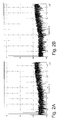
- FIGS. 2A and 2B show two amplitude spectra for one typical use case in the audio field for the UWPM method (Fig. 2A) or a signal processing according to the present Method (FIG. 2B).
- the amplitude spectrum corresponds to a 1 kHz signal from a frequency range from 0 ... 50 kHz for a corresponding PCM-to-PWM converter.
- Fig. 2A shows large harmonic in the low frequency range Vibration components, as in a conversion according to UPWM usually occur. These can be below no longer be filtered out, as they are in the interest Frequency band are located.
- Fig. 2B shows the spectrum of a Conversion according to the presently described method according to the empirically reduced equation (2). Visible is the good linearity of the conversion process, with the big ones harmonic vibrations do not occur, thus at one later signal processing not or only to a lesser extent must be taken into account.
Landscapes
- Engineering & Computer Science (AREA)
- Theoretical Computer Science (AREA)
- Multimedia (AREA)
- Signal Processing (AREA)
- Power Engineering (AREA)
- Analogue/Digital Conversion (AREA)
- Compression, Expansion, Code Conversion, And Decoders (AREA)
- Amplifiers (AREA)
Abstract
Description
- Fig. 1
- schematisch Komponenten für eine PCM-zu-PWM-Umwandlung; und
- Fig. 2A, 2B
- Amplitudenspektren einer PCM-zu-PWM-Umwandlung gemäß dem UPWM-Verfahren gegenüber einer Umwandlung mit einer Anordnung und Verfahrensweise gemäß Fig. 1.

5,245,593, 5,559,467, 5,959,501, 6,014,055, 6,181,266 B1, 6,414,613 B1, 6,430,220 B1, 6,473,009 B1, 6,473,457 B1, 6,518,838 B1, 2002/0036579 A1, 2002/0041246 A1, 2002/0060605 A1, 2002/0135419 A1, 2003/0006838 A1, 2003/0031245 A1, 2003/0042868 A1.
Claims (12)
- Verfahren zum Umwandeln eines digitalen kodierten Signals (PCM, f(t)), insbesondere pulskodierten Signals, in ein pulsweiten-moduliertes Signal (PWM), bei dem das digitale Signal (PCM, f(t)) mit zumindest einer Ableitung (f'(t), f''(t),..., f(n)(t)) des Signals (f(t)) multipliziert wird.
- Verfahren nach Anspruch 1, bei dem das umgewandelte Signal (t0; PWM) aus linearen und/oder nicht-linearen Termen gebildet wird, wobei zumindest ein Teil der Terme eine Ableitung höherer Ordnung aufweist.
- Verfahren nach Anspruch 1 oder 2, bei dem das umgewandelte Signal (t0; PWM) aus Termen mit Ableitungen niedriger, insbesondere maximal zweiter Ordnung gebildet wird.
- Verfahren nach einem vorstehenden Anspruch, bei den Ableitungen (f'(t), f''(t),...) mit Wichtungsfaktoren (b0, ..., bn+1) gewichtet werden.
- Verfahren nach Anspruch 4, bei dem die Wichtungsfaktoren (b0, b1, ....., bn+1) eine Auflösung weniger Bit aufweisen.
- Verfahren nach einem vorstehenden Anspruch, bei dem für das Umwandeln ein empirisch reduzierter Satz aus Termen verwendet wird, insbesondere gemäßwobei f(t) für die Signalamplitude des digitalen Eingangssignals steht, f'(t) für die erste Ableitung dieses Signals f(t), f''(t) für die zweite Ableitung dieses Signals, a0, b0, b1, b2, b3 für Wichtungsfaktoren.

- Verfahren nach einem vorstehenden Anspruch, bei dem die Berechnung zum Umwandeln nicht-iterativ und divisionsfrei durch Additionen und Multiplikationen durchgeführt wird.
- Verfahren zum Umwandeln eines digitalen kodierten Signals (PCM), insbesondere pulskodierten Signals, in ein pulsweiten-moduliertes Signal (PWM), insbesondere nach einem Verfahren nach einem der vorstehenden Ansprüche, bei dem zum Erzielen einer für das pulsweiten-modulierte Signal ausreichenden Abtastrate eine Überabtastung des digitalen Signals zu einem erforderlichen Überabtastfaktor durchgeführt wird,
dadurch gekennzeichnet, dass
eine Überabtastung mit einem Überabtastfaktor vor und eine Überabtastung mit einem weiteren Überabtastfaktor nach dem Umwandeln derart durchgeführt wird, dass das Produkt der Überabtastfaktoren vor und nach dem Umwandeln des digitalen Signals in das pulsweiten-modulierte Signal mindestens dem Wert des abschließend erforderlichen Überabtastfaktors entspricht. - Vorrichtung zum Umwandeln eines digitalen kodierten Signals (PCM, f(t)), insbesondere pulskodierten Signals, in ein pulsweiten-moduliertes Signal (PWM, t0), insbesondere mit einem Verfahren nach einem der Ansprüche 1 - 9, mit einer Schaltungsanordnung (5) zum Berechnen des pulsweiten-modulierten Signals aus Termen mit Ableitungen (f'(t), f''(t), ..., f(n)(t)) des digitalen Signals (f(t)) und Multiplikationen der Ableitungen mit dem digitalen Signal (f(t)).
- Vorrichtung nach Anspruch 9, bei der die Schaltungsanordnung (5) zum Berechnen des pulsweiten-modulierten Signals ausschließlich Multiplikationsglieder, Additionsglieder und Zwischenspeicher aufweist.
- Vorrichtung nach Anspruch 9 oder 10, bei der die Schaltungsanordnung (5) ohne Divisionsglieder zum Berechnen der Umwandlung aufgebaut ist.
- Vorrichtung insbesondere nach einem der Ansprüche 9-11 und/oder zum Durchführen eines Verfahrens nach einem der Ansprüche 1-8, mitgekennzeichnet durcheiner Überabtasteinrichtung zum Überabtasten eines digitalen kodierten Signals (PCM) insbesondere pulskodierten Signals,einer Schaltungsanordnung (5) zum Berechnen eines pulsweiten-modulierten Signals (PWM) oder einer Vorstufe davon undeinem Generator zum Bereitstellen eines pulsweiten-modulierten Ausgangssignals (PWM),eine zweite Überabtasteinrichtung (6), welche der Schaltungsanordnung (5) nachgeschaltet ist, wobei das Produkt der Überabtastfaktoren der Überabtasteinrichtungen (4, 6) vor und nach der Schaltungsanordnung (5) mindestens einem Wert eines erforderlichen Überabtastfaktors zum Bereitstellen einer PWM-Wiederholungsrate für das pulsweiten-modulierte Ausgangssignal (PWM) entspricht.
Applications Claiming Priority (4)
| Application Number | Priority Date | Filing Date | Title |
|---|---|---|---|
| US48700003P | 2003-07-14 | 2003-07-14 | |
| US487000P | 2003-07-14 | ||
| DE10337782A DE10337782B4 (de) | 2003-07-14 | 2003-08-14 | Methode und Schaltung zur effektiven Konvertierung von PCM-in PWM-Daten |
| DE10337782 | 2003-08-14 |
Publications (2)
| Publication Number | Publication Date |
|---|---|
| EP1498803A2 true EP1498803A2 (de) | 2005-01-19 |
| EP1498803A3 EP1498803A3 (de) | 2007-04-04 |
Family
ID=33477530
Family Applications (1)
| Application Number | Title | Priority Date | Filing Date |
|---|---|---|---|
| EP04006659A Withdrawn EP1498803A3 (de) | 2003-07-14 | 2004-03-19 | Methode und Schaltung zur effektiven Konvertierung vom PCM- in PWM-Daten |
Country Status (4)
| Country | Link |
|---|---|
| EP (1) | EP1498803A3 (de) |
| JP (1) | JP4189757B2 (de) |
| KR (1) | KR100894583B1 (de) |
| CN (1) | CN1617455B (de) |
Cited By (1)
| Publication number | Priority date | Publication date | Assignee | Title |
|---|---|---|---|---|
| FR2915036A1 (fr) * | 2007-04-13 | 2008-10-17 | Anagram Technologies | Dispositif de modulation de signaux en largeurs d'impulsions a trois niveaux et amplificateur numerique mettant en oeuvre un tel dispositif. |
Families Citing this family (3)
| Publication number | Priority date | Publication date | Assignee | Title |
|---|---|---|---|---|
| CN101789258B (zh) * | 2010-04-02 | 2013-01-23 | 福州思迈特数码科技有限公司 | 采用纯数字音频处理的车载dvd导航影音装置 |
| JP6249204B2 (ja) * | 2013-04-22 | 2017-12-20 | 国立大学法人 名古屋工業大学 | パルス幅変調信号生成器およびフルデジタルアンプおよびデジタル−アナログ変換器 |
| CN109188896B (zh) * | 2018-08-30 | 2019-08-09 | 华南理工大学 | 一种非均匀过采样数字控制器及其控制方法 |
Citations (1)
| Publication number | Priority date | Publication date | Assignee | Title |
|---|---|---|---|---|
| US5617058A (en) * | 1995-11-13 | 1997-04-01 | Apogee Technology, Inc. | Digital signal processing for linearization of small input signals to a tri-state power switch |
Family Cites Families (7)
| Publication number | Priority date | Publication date | Assignee | Title |
|---|---|---|---|---|
| KR0150206B1 (ko) * | 1989-02-21 | 1998-12-15 | 오가 노리오 | 디지탈/아날로그 변환기 |
| GB9027503D0 (en) * | 1990-12-19 | 1991-02-06 | Sandler Mark B | Improvements in or relating to digital to analogue conversion |
| GB9103777D0 (en) * | 1991-02-22 | 1991-04-10 | B & W Loudspeakers | Analogue and digital convertors |
| EA002110B1 (ru) * | 1996-03-28 | 2001-12-24 | ТЕКСАС ИНСТРУМЕНТС, КОПЕНГАГЕН АпС | Преобразование сигнала с импульсно-кодовой модуляцией в сигнал с широтно-импульсной модуляцией с равномерным распределением |
| JP3388143B2 (ja) * | 1997-07-12 | 2003-03-17 | 株式会社ケンウッド | D/a変換回路 |
| US6430220B1 (en) * | 2000-09-19 | 2002-08-06 | Apogee Technology Inc. | Distortion reduction method and apparatus for linearization of digital pulse width modulation by efficient calculation |
| US6606044B2 (en) * | 2002-01-02 | 2003-08-12 | Motorola, Inc. | Method and apparatus for generating a pulse width modulated signal |
-
2004
- 2004-03-19 EP EP04006659A patent/EP1498803A3/de not_active Withdrawn
- 2004-05-11 CN CN2004100445181A patent/CN1617455B/zh not_active Expired - Fee Related
- 2004-05-25 JP JP2004154373A patent/JP4189757B2/ja not_active Expired - Fee Related
- 2004-07-07 KR KR1020040052642A patent/KR100894583B1/ko not_active Expired - Fee Related
Patent Citations (1)
| Publication number | Priority date | Publication date | Assignee | Title |
|---|---|---|---|---|
| US5617058A (en) * | 1995-11-13 | 1997-04-01 | Apogee Technology, Inc. | Digital signal processing for linearization of small input signals to a tri-state power switch |
Cited By (2)
| Publication number | Priority date | Publication date | Assignee | Title |
|---|---|---|---|---|
| FR2915036A1 (fr) * | 2007-04-13 | 2008-10-17 | Anagram Technologies | Dispositif de modulation de signaux en largeurs d'impulsions a trois niveaux et amplificateur numerique mettant en oeuvre un tel dispositif. |
| WO2008125403A1 (fr) * | 2007-04-13 | 2008-10-23 | Anagram Technologies Sa | Dispositif de modulation de signaux en largeurs d'impulsions à trois niveaux et amplificateur numérique mettant en oeuvre un tel dispositif |
Also Published As
| Publication number | Publication date |
|---|---|
| KR100894583B1 (ko) | 2009-04-24 |
| CN1617455A (zh) | 2005-05-18 |
| KR20050009143A (ko) | 2005-01-24 |
| EP1498803A3 (de) | 2007-04-04 |
| CN1617455B (zh) | 2010-06-23 |
| JP4189757B2 (ja) | 2008-12-03 |
| JP2005039789A (ja) | 2005-02-10 |
Similar Documents
| Publication | Publication Date | Title |
|---|---|---|
| DE69123366T2 (de) | Digitale Rauschformerschaltung | |
| DE69737882T2 (de) | Umwandlung eines pcm-signals in ein gleichmässig pulsbreitenmoduliertes signal | |
| DE60007087T2 (de) | Verfahren und gerät zur korrektur von delta-sigma-wandlern hoher ordnung | |
| DE69228987T2 (de) | Analog-und digitalwandler | |
| DE69230551T2 (de) | Verfahren und Gerät zur Erzeugung von Korrektionssignalen zur Bildung von analogen Signalen mit niedriger Verzerrung | |
| DE69422046T2 (de) | Digital-analog-wandler mit überabtastung | |
| EP0052847B1 (de) | Verfahren und Schaltungsanordnung zur Umsetzung der Abtastfrequenz einer Abtastfolge unter Umgehung der Konversion in ein kontinuierliches Signal | |
| DE60001148T2 (de) | Schaltung zur rausch- und fehlerkompensation der ausgangsstufe eines digitalen verstärkers | |
| DE4233738C2 (de) | Digitaler Interpolator und Verfahren zur Interpolation digitaler Daten | |
| DE69919500T2 (de) | PWM Leistungsverstärker mit digitalem Eingang | |
| DE68915700T2 (de) | Verfahren zur Kaskadierung von mehreren Sigma-Delta-Modulatoren und ein Sigma-Delta-Modulatorsystem. | |
| DE3486102T2 (de) | Gerät und Verfahren zur AD- und DA-Umwandlung. | |
| DE3510660C2 (de) | ||
| DE69029751T2 (de) | Digital-Analogwandler | |
| DE112013000926B4 (de) | Sigma-Delta-Modulator mit Dithersignal | |
| DE112012000529T5 (de) | Direkte Rückkopplung für zeitkontinuierliche überabgetastete Wandler | |
| DE102008026115A1 (de) | Impulsbreitenmodulator, welcher einen Interpolator verwendet | |
| DE10337782B4 (de) | Methode und Schaltung zur effektiven Konvertierung von PCM-in PWM-Daten | |
| EP1001538A2 (de) | Sigma-Delta-Modulator und Verfahren zur Unterdrückung eines Quantisierungsfehlers in einem Sigma-Delta-Modulator | |
| DE69114129T2 (de) | Dezimationsfilter für Sigma-Delta Konverter und Datenendeinrichtung mit einem solchen Filter. | |
| WO2004068703A1 (de) | Vorrichtung und verfahren zur digitalen pulsweiten-modulation | |
| EP1498803A2 (de) | Methode und Schaltung zur effektiven Konvertierung vom PCM- in PWM-Daten | |
| EP2856642B1 (de) | Geschalteter verstärker für variable versorgungsspannung | |
| DE10327620B4 (de) | Vorrichtung und Verfahren zur digitalen Pulsweiten-Modulation | |
| DE69832770T2 (de) | Delta-Sigma-Modulator |
Legal Events
| Date | Code | Title | Description |
|---|---|---|---|
| PUAI | Public reference made under article 153(3) epc to a published international application that has entered the european phase |
Free format text: ORIGINAL CODE: 0009012 |
|
| AK | Designated contracting states |
Kind code of ref document: A2 Designated state(s): AT BE BG CH CY CZ DE DK EE ES FI FR GB GR HU IE IT LI LU MC NL PL PT RO SE SI SK TR |
|
| AX | Request for extension of the european patent |
Extension state: AL LT LV MK |
|
| RIC1 | Information provided on ipc code assigned before grant |
Ipc: H03M 1/82 20060101ALN20061228BHEP Ipc: H03M 1/06 20060101ALI20061228BHEP Ipc: G11B 20/10 20060101ALI20061228BHEP Ipc: H03M 5/08 20060101ALI20061228BHEP Ipc: G06F 1/26 20060101AFI20041108BHEP |
|
| PUAL | Search report despatched |
Free format text: ORIGINAL CODE: 0009013 |
|
| AK | Designated contracting states |
Kind code of ref document: A3 Designated state(s): AT BE BG CH CY CZ DE DK EE ES FI FR GB GR HU IE IT LI LU MC NL PL PT RO SE SI SK TR |
|
| AX | Request for extension of the european patent |
Extension state: AL LT LV MK |
|
| RIC1 | Information provided on ipc code assigned before grant |
Ipc: H03M 1/82 20060101ALN20061228BHEP Ipc: H03F 3/217 20060101ALI20070223BHEP Ipc: H03M 1/06 20060101ALI20070223BHEP Ipc: G11B 20/10 20060101ALI20070223BHEP Ipc: H03M 5/08 20060101ALI20070223BHEP Ipc: G06F 1/26 20060101AFI20041108BHEP |
|
| 17P | Request for examination filed |
Effective date: 20070623 |
|
| 17Q | First examination report despatched |
Effective date: 20070723 |
|
| AKX | Designation fees paid |
Designated state(s): DE FR GB IT NL |
|
| RAP1 | Party data changed (applicant data changed or rights of an application transferred) |
Owner name: TRIDENT MICROSYSTEMS (FAR EAST) LTD. |
|
| RAP1 | Party data changed (applicant data changed or rights of an application transferred) |
Owner name: ENTROPIC COMMUNICATIONS, INC. |
|
| STAA | Information on the status of an ep patent application or granted ep patent |
Free format text: STATUS: THE APPLICATION IS DEEMED TO BE WITHDRAWN |
|
| 18D | Application deemed to be withdrawn |
Effective date: 20131001 |