EP1500218B1 - Mesure et compensation de dispersion chromatique - Google Patents
Mesure et compensation de dispersion chromatique Download PDFInfo
- Publication number
- EP1500218B1 EP1500218B1 EP03710212A EP03710212A EP1500218B1 EP 1500218 B1 EP1500218 B1 EP 1500218B1 EP 03710212 A EP03710212 A EP 03710212A EP 03710212 A EP03710212 A EP 03710212A EP 1500218 B1 EP1500218 B1 EP 1500218B1
- Authority
- EP
- European Patent Office
- Prior art keywords
- optical
- signal
- dispersion
- wavelength
- line
- Prior art date
- Legal status (The legal status is an assumption and is not a legal conclusion. Google has not performed a legal analysis and makes no representation as to the accuracy of the status listed.)
- Expired - Lifetime
Links
- 239000006185 dispersion Substances 0.000 title claims abstract description 107
- 238000005259 measurement Methods 0.000 title 1
- 230000003287 optical effect Effects 0.000 claims abstract description 121
- 238000000034 method Methods 0.000 claims abstract description 33
- 238000012544 monitoring process Methods 0.000 claims abstract description 21
- 238000004891 communication Methods 0.000 claims abstract description 16
- 230000005540 biological transmission Effects 0.000 claims description 6
- 230000001360 synchronised effect Effects 0.000 claims description 4
- 239000000835 fiber Substances 0.000 description 24
- 238000010586 diagram Methods 0.000 description 12
- 238000012937 correction Methods 0.000 description 5
- 230000000694 effects Effects 0.000 description 5
- 230000008859 change Effects 0.000 description 3
- 230000007246 mechanism Effects 0.000 description 3
- 239000013307 optical fiber Substances 0.000 description 3
- 230000001276 controlling effect Effects 0.000 description 2
- 230000002596 correlated effect Effects 0.000 description 2
- 230000000875 corresponding effect Effects 0.000 description 2
- 230000001934 delay Effects 0.000 description 2
- 230000009022 nonlinear effect Effects 0.000 description 2
- 230000000737 periodic effect Effects 0.000 description 2
- 230000010363 phase shift Effects 0.000 description 2
- 238000012545 processing Methods 0.000 description 2
- 230000003213 activating effect Effects 0.000 description 1
- 230000003044 adaptive effect Effects 0.000 description 1
- 230000001419 dependent effect Effects 0.000 description 1
- 238000005516 engineering process Methods 0.000 description 1
- 230000001939 inductive effect Effects 0.000 description 1
- 230000003993 interaction Effects 0.000 description 1
- 230000009021 linear effect Effects 0.000 description 1
- 230000008569 process Effects 0.000 description 1
- 238000011084 recovery Methods 0.000 description 1
- 230000035945 sensitivity Effects 0.000 description 1
- 230000003595 spectral effect Effects 0.000 description 1
- 230000007704 transition Effects 0.000 description 1
Images

Classifications
-
- G—PHYSICS
- G01—MEASURING; TESTING
- G01M—TESTING STATIC OR DYNAMIC BALANCE OF MACHINES OR STRUCTURES; TESTING OF STRUCTURES OR APPARATUS, NOT OTHERWISE PROVIDED FOR
- G01M11/00—Testing of optical apparatus; Testing structures by optical methods not otherwise provided for
- G01M11/30—Testing of optical devices, constituted by fibre optics or optical waveguides
- G01M11/33—Testing of optical devices, constituted by fibre optics or optical waveguides with a light emitter being disposed at one fibre or waveguide end-face, and a light receiver at the other end-face
- G01M11/333—Testing of optical devices, constituted by fibre optics or optical waveguides with a light emitter being disposed at one fibre or waveguide end-face, and a light receiver at the other end-face using modulated input signals
-
- G—PHYSICS
- G01—MEASURING; TESTING
- G01M—TESTING STATIC OR DYNAMIC BALANCE OF MACHINES OR STRUCTURES; TESTING OF STRUCTURES OR APPARATUS, NOT OTHERWISE PROVIDED FOR
- G01M11/00—Testing of optical apparatus; Testing structures by optical methods not otherwise provided for
- G01M11/30—Testing of optical devices, constituted by fibre optics or optical waveguides
- G01M11/33—Testing of optical devices, constituted by fibre optics or optical waveguides with a light emitter being disposed at one fibre or waveguide end-face, and a light receiver at the other end-face
- G01M11/335—Testing of optical devices, constituted by fibre optics or optical waveguides with a light emitter being disposed at one fibre or waveguide end-face, and a light receiver at the other end-face using two or more input wavelengths
-
- G—PHYSICS
- G01—MEASURING; TESTING
- G01M—TESTING STATIC OR DYNAMIC BALANCE OF MACHINES OR STRUCTURES; TESTING OF STRUCTURES OR APPARATUS, NOT OTHERWISE PROVIDED FOR
- G01M11/00—Testing of optical apparatus; Testing structures by optical methods not otherwise provided for
- G01M11/30—Testing of optical devices, constituted by fibre optics or optical waveguides
- G01M11/33—Testing of optical devices, constituted by fibre optics or optical waveguides with a light emitter being disposed at one fibre or waveguide end-face, and a light receiver at the other end-face
- G01M11/338—Testing of optical devices, constituted by fibre optics or optical waveguides with a light emitter being disposed at one fibre or waveguide end-face, and a light receiver at the other end-face by measuring dispersion other than PMD, e.g. chromatic dispersion
-
- G—PHYSICS
- G02—OPTICS
- G02B—OPTICAL ELEMENTS, SYSTEMS OR APPARATUS
- G02B6/00—Light guides; Structural details of arrangements comprising light guides and other optical elements, e.g. couplings
- G02B6/24—Coupling light guides
- G02B6/26—Optical coupling means
- G02B6/28—Optical coupling means having data bus means, i.e. plural waveguides interconnected and providing an inherently bidirectional system by mixing and splitting signals
- G02B6/293—Optical coupling means having data bus means, i.e. plural waveguides interconnected and providing an inherently bidirectional system by mixing and splitting signals with wavelength selective means
- G02B6/29379—Optical coupling means having data bus means, i.e. plural waveguides interconnected and providing an inherently bidirectional system by mixing and splitting signals with wavelength selective means characterised by the function or use of the complete device
- G02B6/29392—Controlling dispersion
- G02B6/29394—Compensating wavelength dispersion
-
- H—ELECTRICITY
- H04—ELECTRIC COMMUNICATION TECHNIQUE
- H04B—TRANSMISSION
- H04B10/00—Transmission systems employing electromagnetic waves other than radio-waves, e.g. infrared, visible or ultraviolet light, or employing corpuscular radiation, e.g. quantum communication
- H04B10/25—Arrangements specific to fibre transmission
- H04B10/2507—Arrangements specific to fibre transmission for the reduction or elimination of distortion or dispersion
- H04B10/2513—Arrangements specific to fibre transmission for the reduction or elimination of distortion or dispersion due to chromatic dispersion
- H04B10/25133—Arrangements specific to fibre transmission for the reduction or elimination of distortion or dispersion due to chromatic dispersion including a lumped electrical or optical dispersion compensator
Definitions
- the invention relates to a method and a system for compensating chromatic dispersion in optical communication lines.
- any optical pulse signal Due to the final spectral width of any optical pulse signal, different parts of the signal will propagate through the fiber with different velocities causing pulse distortion, which will be called the signal dispersion in the frame of the present application.
- various effects appear. For example, such effects are caused by mutual interference between adjacent optical pulses within the optical channel (so-called inter-symbol interference ISI), and decrease and spread the pulse peak.
- ISI inter-symbol interference
- DCF dispersion compensating fibers
- One alternative technique for compensating the fiber dispersion uses chirped periodic structures to create different delays between signals of different wavelengths and therefore to compensate for the fiber chromatic dispersion.
- This technique is presented today by the chirped fiber Bragg gratings, for example described in a Japanese patent application JP 20002 35170 A . Arrangements belonging to this technique do not create non-linear interactions, the gratings have a small size and allow for creation of variable compensation modules.
- US 6,252,692 describes an optical transmission system including means for measuring optical dispersion in an optical path, and a controllable element such as a dispersion compensator, operable in dependence on the measured value of dispersion.
- a low frequency dither on the optical signal causes timing jitter which varies according to the dispersion in the optical path.
- the timing jitter is extracted from a clock signal recovered from the optical signal. This jitter is correlated with the original dither to remove jitter effects caused by other mechanisms.
- the dispersion determining means comprises means for impressing a pattern on the transmitted signal; the system also comprises correlating means to correlate the timing jitter with this pattern. Provided that the pattern is asymmetric, the correlating means are arranged to determine the sign of the dispersion value.
- the object of the invention is to provide another technique for determining the sign of chromatic dispersion in an optical line and a suitable technique for the chromatic dispersion compensation.
- the above object can be achieved by determining the sign of chromatic dispersion in an optical communication line suitable for transmitting an optical signal at a predetermined optical wavelength, the method comprising steps of:
- the method additionally comprises transmitting data via the optical communication line using, as a carrier, the optical signal at the changing wavelength; in this version, the second signal reflects changes of delay of the data transmitted with said optical signal via said line.
- the optical communication line preferably constitutes an optical fiber.
- another method for compensating chromatic dispersion in the optical communication line, which additionally comprises the following cyclically repeating step: based on a currently determined sign of dispersion, introducing a dispersion increment having the opposite sign, up to achieving in the optical communication line the sign of the dispersion opposite to said currently determined.
- the method proposes catching a zero dispersion crossing point based on the dispersion sign transition, and using that as a control mechanism for obtaining a compensated, zero dispersion telecommunication line.
- dispersion of the optical communication line can be kept close to a specific value. It can be done, say, when an over- or under-compensation of dispersion is required due to the presence of non-linear effects in the optical line. For example, it can be performed by introducing at a transmission site a delay variation synchronized with variation in the wavelength so as to create an offset in the delay variation at the receiving site. Therefore, the "detected zero crossing" will be offset to a particular pre-calibrated value.
- the dispersion increment used in the method can be selected so as to provide fast and/or accurate compensation of the line dispersion and keeping it as close as possible to the selected value (zero or whatever selected). Technologies of selecting the dispersion increment are not discussed in the frame of the present application.
- the above-proposed method of the dispersion compensation is particularly applicable to high speed networks, for example those transmitting data at about 40 Gbps and above. At such bitrates small fluctuations in dispersion are critical and therefore the control mechanism should track them.
- both the method of determining the dispersion sign and the method of compensating the dispersion are performed continuously and automatically.
- the method may comprise (in one specific version):
- the power of the optical signal may be performed by performing current modulation of the laser producing the optical signal, or modulation of power of the optical signal after being emitted from the laser, using an external modulator.
- the amplitude of this modulating signal should be correlated to the wavelength of the optical carrier.
- the power of the optical signal can be monitored to determine the wavelength changes.
- the monitoring of the wavelength changes can be performed by applying the optical signal to interferometer at the receiving site, or by using a filter having attenuation sensitivity depending on the signal wavelength.
- phase lock loop PLL circuit
- corrections of the phase are provided and such corrections speak for changes of phase of the optical signal which take place due to dispersion changes in the transmission line.
- PLL phase lock loop
- the step of comparing the first signal with the second signal is accompanied by processing the resulting phase difference to determine the dispersion sign and preferably followed by applying, to the optical line, a pre-selected dispersion increment with a sign opposite to the determined one.
- This can be provided by controlling an in-line dispersion compensation element.
- the system should include a receiving node, a transmitting node and an optical communication line connecting said nodes and suitable for transmitting an optical carrier signal at a particular wavelength, wherein the transmitting node comprises means for changing wavelength of the optical carrier signal around said particular wavelength at a predetermined manner (preferably periodically), the receiving node comprises:
- the system also comprises means for transmitting data via said optical line using, as a carrier, said optical signal having the changing wavelength.
- the system also includes a dynamic dispersion compensation unit (DDCU) inserted in the optical line, anywhere before the receiving node and controllable by said phase comparator.
- DDCU dynamic dispersion compensation unit
- the dynamic dispersion compensation unit is adapted to ensure zero dispersion in the optical signal incoming the receiver.
- the node equipment comprising a transmitter portion and a receiver portion, contains at its receiver portion:
- the node additionally comprises a dispersion compensating device controllable by said comparator.
- the first signal at the receiver portion of the discussed node can be produced by AM demodulation.
- the equipment for monitoring phase changes in the received optical signal may, for example, comprises a CDR (Clock and Data Recovery) circuit which usually comprises a PLL (Phase Lock Loop) circuit as a part thereof.
- the CDR circuit may be part of an electrical deserializer (demultiplexer). Functionality of the PLL circuit is known to those skilled in the art, though such a circuit has never been used for the purpose set in the present invention.
- the mentioned equipment is preferably provided per each optical channel in the receiver portion of the node.
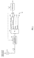
- Fig. 1 illustrates an embodiment of a system 10 implementing the method according to the invention for determining a sign of chromatic dispersion in an optical line.
- the system 10 can be called a dispersion sign monitor and may optionally perform automatic dispersion compensation.
- a transmitter Tx 12 transmits, via an optical fiber line 14, an optical signal at a carrier wavelength ⁇ (the optical signal suitable for carrying data).
- ⁇ the optical signal suitable for carrying data
- data is transmitted using the optical carrier signal.
- the wavelength is modulated at the transmitter 12, say, using a small dither.
- a receiver Rx marked 16 upon receiving an input optical signal, provides a number of outputs including: data output 18, clock output 20, ⁇ -monitoring output 22 and phase monitoring output 24.
- the illustrated number of outputs is exemplary and non-exhaustive.
- the output 22 carries a signal (a first monitoring signal S1) reflecting changes of the carrier wavelength, if such occur.
- the output 24 carries a signal (a second monitoring signal S2) which represents the optical signal delay. If data is transmitted via the line. the signal 24 represents the data delay. So, if any changes of chromatic dispersion take place, that will be reflected in the second signal S2.
- the sign of the dispersion can be determined knowing the phase relation between the wavelength changes and the data delay, i.e., between signal S1 and signal S2.
- characteristic changes of the data delay will be shown in some of Figs. 3 to demonstrate clear dependence thereof on the sign of dispersion of the transmission line.
- a phase comparator 26 compares the first and the second monitoring signals thus producing a third signal S3 which can be used for determining the sign of the dispersion.
- S3 is translated by a processor 28 which, firstly, is able to explicitly obtain the sign of the dispersion.
- the processor 28 is capable of producing, according to a predetermined algorithm, a signal S4 which can be used for controlling a dispersion compensation block 29 which is positioned anywhere in the fiber between the transmitter 12 and the receiver 16, and terminates a feedback loop of the dispersion sign monitor 10.
- the signal S4 is informative both on the direction (sign) and the amount of the dispersion to be corrected.
- the amount of correction is a pre-selected dispersion increment which is sufficiently small to achieve the accurate dispersion compensation.
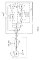
- Fig. 2 illustrates one particular embodiment 30 of the dispersion sign monitor shown in Fig. 1 .
- the transmitter portion 32 comprises, for example, a DFB (Distributed Feedback laser) 34, followed by a modulator 36 which modulates the carrier wavelength produced by the laser 34 by high rate data.
- the transmitter portion is provided with a dither block 38.
- the current of the DFB laser is modulated using a sinusoidal dither added to the laser bias current.
- the dither creates modulation of optical power and wavelength ⁇ at the output of the DFB laser, the wavelength change occurs due to a so-called adiabatic chirp.
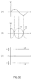
- Time diagrams of the parameters at point (A) of the monitor are shown in Fig. 3A as follows: the changing wavelength ⁇ is shown as Fig. 3A (1), and the carrier wavelength optical signal, with its dither modulated power around a given power P o is shown in Fig. 3A (2).
- the carrier wavelength optical signal is then passed through the external modulator 36 where it is modulated by data at high bit rate (say, 40 Gbps).
- the wavelength continues to change as it did at point A (the diagram 3B(1)).
- the resulting optical signal obtained upon the data modulation at point (B) is presented by the time diagram 3B(2).
- the optical signal carries a sequence of "1" and "0" intervals, according to the data impressed by the modulator 36. (The relative time scale representation of the dither and data is intentionally exaggerated to facilitate the explanation).
- the wavelength-shift due to the dispersion of the fiber, creates phase shift in the base-band signal, which can be seen as the data delay.
- the dither current added to the laser bias current has a sine waveform I 0 sin( ⁇ B t) modulated at angular frequency ⁇ B and amplitude I 0
- FIG. 3D It can be shown in the following figure 3D .
- the figure illustrates that T(t) is synchronous with the changing carrier wavelength ⁇ .
- the solid line represents behavior of the delay when the dispersion is positive, and the dotted line - when the dispersion is negative.
- equipment of a network node according to the invention is schematically marked 41.
- the modulated optical signal is interpreted in two detectors: AM detector 44 and PLL 46 used as a phase detector.
- the PLL is used to track the phase variation of the input signal, thus the signal at the output of the Loop Filter 43 (point K) represents a time derivative of the phase due to operation of VCO 45 (Voltage Controlled Oscillator) which acts as a phase integrator.
- VCO 45 Voltage Controlled Oscillator
- This signal thus contains noise at all frequencies and has to be filtered using the band-pass filter BPF 47 of the PLL detector 46.
- the filtered signal is marked S2 and has a phase shift of ⁇ /2 due to the derivative operation described above.
- the AM detector 44 is a simple band-pass filter (BPF) which filters out the AM tone and forms the first signal S1.
- This tone, S1 is further phase compared to the tone S2.
- a phase comparator PC 48 determines the sign of the dispersion monitored. Schematically, this process is shown in Fig. 3E , where the signal S1 (3E(1)) is compared to signal S2 (3E(2), solid line) being the derivative of the delay signal, at a positive dispersion of the fiber line.
- the S2 in the case of a negative dispersion is shown as the symmetric dotted curve at the same diagram.
- phase comparator (PC) 48 obtains the phase difference (S2 - S1) and determines the sign of the dispersion D.
- the basis of the decision making is illustrated in Fig. 3E (3).
- the phase difference between S1 and S2 will always be a fixed but random phase due to a phase introduced by all electrical components of the circuit.
- the phase difference detected between S1 and S2 will always constitute a difference of " ⁇ " between the cases of positive and negative dispersion.
- the PC 48 is capable of activating a Dispersion Compensating block 50 for correcting the received optical signal.
- the PC 48 or the block 50 may comprise processing means for selecting a proper dispersion increment for further compensation of the dispersion.
- the increment may have an adaptive step size.
- the block 50 may repetitively introduce into the optical fiber line a pre-selected or a changing dispersion increment having the opposite sign up to the moment when the sign of dispersion in the line changes. From that moment, the correction will automatically be performed in the opposite direction, so the dispersion is dynamically kept close to zero.
- the correction can be performed so as to maintain any pre-selected dispersion value. It can be performed, for example, by inducing a delay variation at the transmission site, synchronized to the wavelength variations.
Landscapes
- Physics & Mathematics (AREA)
- Chemical & Material Sciences (AREA)
- Optics & Photonics (AREA)
- General Physics & Mathematics (AREA)
- Analytical Chemistry (AREA)
- Dispersion Chemistry (AREA)
- Electromagnetism (AREA)
- Engineering & Computer Science (AREA)
- Computer Networks & Wireless Communication (AREA)
- Signal Processing (AREA)
- Optical Communication System (AREA)
- Eye Examination Apparatus (AREA)
- Spectrometry And Color Measurement (AREA)
- Light Guides In General And Applications Therefor (AREA)
- Investigating Or Analysing Materials By Optical Means (AREA)
Claims (10)
- Procédé de détermination du signe de dispersion chromatique dans une ligne de communication optique (14, 40) apte à transmettre un signal optique à une longueur d'onde optique prédéterminée, le procédé comprenant les étapes consistant à :introduire des changements contrôlés de longueur d'onde autour de ladite longueur d'onde prédéterminée,surveiller le signal optique ayant traversé ladite ligne, et étant caractérisé en ce qu'il consiste à obtenir- un premier signal (S1) indiquant des changements de la longueur d'onde porteuse dudit signal optique,- un second signal (S2) indiquant des changements de retard dudit signal optique transmis par l'intermédiaire de ladite ligne,à comparer le premier signal avec le second signal, età déterminer le signe de dispersion chromatique en fonction de la différence de phase entre les premier et second signaux comparés.
- Procédé selon la revendication 1, consistant en outre à transmettre des données par l'intermédiaire de la ligne de communication optique en utilisant, comme porteuse, le signal optique à la longueur d'onde changeante ; dans le procédé, le second signal indique des changements de retard des données transmises avec ledit signal optique par l'intermédiaire de ladite ligne.
- Procédé selon la revendication 1 ou 2, comprenant en outre l'étape répétée de façon cyclique qui consiste :en fonction du signe de dispersion déterminé, à introduire un incrément de dispersion ayant le signe opposé, jusqu'à ce que le signe opposé de la dispersion soit déterminé dans la ligne de communication optique,afin de compenser la dispersion chromatique dans la ligne de communication optique.
- Procédé selon la revendication 1 ou 2, comprenant en outre les étapes consistant à :introduire au niveau d'un site de transmission (32) une variation de retard synchronisée avec une variation de la longueur d'onde de manière à créer un décalage du retard au niveau d'un site de réception (41),en fonction du signe de dispersion déterminé, à introduire un incrément de dispersion ayant le signe opposé, jusqu'à ce que le signe opposé de la dispersion soit déterminé dans la ligne de communication optique,afin de maintenir la dispersion de la ligne de communication optique (14, 40) proche d'une valeur spécifique.
- Système (10, 30) de détermination d'un signe de dispersion dans une ligne optique (14, 40), le système comprenant un noeud de réception (41), un noeud de transmission (12, 32) et la ligne optique (14, 40) reliant lesdits noeuds et destinée à transmettre un signal optique à une longueur d'onde de porteuse optique particulière, dans lequel
le noeud de transmission (12, 32) comprend des moyens (38) pour changer de façon contrôlée la longueur d'onde de la porteuse optique autour de ladite longueur d'onde particulière d'une manière prédéterminée, et pour transmettre le signal optique par ladite porteuse optique changeante par l'intermédiaire de la ligne optique, caractérisé en ce que
le noeud de réception comprend :des moyens (22, 44) pour surveiller les changements de longueur d'onde dans le signal optique reçu par l'intermédiaire de la ligne optique, afin de produire un premier signal (S1),des moyens (24, 26) pour surveiller les changements de phase provoqués dans le signal optique reçu par l'intermédiaire de la ligne optique, afin de produire un second signal (S2) ;un comparateur de phases (26, 48) pour comparer la phase du premier signal à la phase du second signal afin de déterminer le signe de dispersion chromatique dans la ligne optique. - Système selon la revendication 5, comprenant en outre des moyens (12, 36) pour transmettre des données par l'intermédiaire de ladite ligne optique en utilisant ledit signal optique ayant la longueur d'onde changeante, comme porteuse.
- Système selon la revendication 5 ou 6, comprenant une unité de compensation de dispersion (29, 50) insérée dans la ligne optique (14, 40) et pouvant être commandée par ledit comparateur de phase (26, 48).
- Equipement de noeud de réception apte à être utilisé dans le système selon l'une quelconque des revendications 5 à 7, le matériel de noeud de réception comprenantdes moyens (22, 44) pour surveiller les changements d'une longueur d'onde porteuse dans un signal optique reçu par l'intermédiaire d'une ligne optique, afin de produire un premier signal (S1),des moyens (24, 26) pour surveiller des changements de phase dans le signal optique reçu par l'intermédiaire de la ligne optique (14, 40), afin de produire un second signal (S2) ;un comparateur de phases (26, 48) pour comparer la phase du premier signal à la phase du second signal afin de déterminer le signe de dispersion chromatique dans la ligne optique.
- Equipement de noeud de réception selon la revendication 8, comprenant en outre un dispositif de compensation de dispersion (29, 50) pouvant être commandé par ledit comparateur de phase (26, 48).
- Equipement de noeud de réception selon la revendication 8 ou 9, dans lequel le premier signal au niveau d'une partie de réception (41) dudit noeud est produit par démodulation AM, à condition que les changements de longueur d'onde contrôlés soient introduits au moyen de la technique de modulation AM au niveau d'une partie de transmission (12, 32) d'un noeud précédent.
Applications Claiming Priority (3)
| Application Number | Priority Date | Filing Date | Title |
|---|---|---|---|
| IL14932402 | 2002-04-24 | ||
| IL149324A IL149324A (en) | 2002-04-24 | 2002-04-24 | Technique for determining sign of optical dispersion in optical communication lines |
| PCT/IL2003/000301 WO2003092194A1 (fr) | 2002-04-24 | 2003-04-10 | Mesure et compensation de dispersion chromatique |
Publications (2)
| Publication Number | Publication Date |
|---|---|
| EP1500218A1 EP1500218A1 (fr) | 2005-01-26 |
| EP1500218B1 true EP1500218B1 (fr) | 2008-07-02 |
Family
ID=28460376
Family Applications (1)
| Application Number | Title | Priority Date | Filing Date |
|---|---|---|---|
| EP03710212A Expired - Lifetime EP1500218B1 (fr) | 2002-04-24 | 2003-04-10 | Mesure et compensation de dispersion chromatique |
Country Status (7)
| Country | Link |
|---|---|
| US (1) | US7064814B2 (fr) |
| EP (1) | EP1500218B1 (fr) |
| AT (1) | ATE400100T1 (fr) |
| AU (1) | AU2003214632A1 (fr) |
| DE (1) | DE60321903D1 (fr) |
| IL (1) | IL149324A (fr) |
| WO (1) | WO2003092194A1 (fr) |
Families Citing this family (8)
| Publication number | Priority date | Publication date | Assignee | Title |
|---|---|---|---|---|
| US8073326B2 (en) * | 2006-12-06 | 2011-12-06 | General Photonics Corporation | Optical polarization division multiplexing in optical communication |
| WO2011083798A1 (fr) * | 2010-01-05 | 2011-07-14 | 日本電気株式会社 | Procédé et appareil destinés à détecter une dispersion en longueur d'onde, et procédé et appareil destinés à compenser une dispersion en longueur d'onde |
| EP2372332B1 (fr) * | 2010-03-31 | 2017-09-06 | Alcatel Lucent | Procédé pour déterminer la dispersion chromatique d'un canal optique |
| JP5605643B2 (ja) * | 2010-12-17 | 2014-10-15 | アイシン精機株式会社 | 波長分散測定装置および波長分散測定方法 |
| JP6220316B2 (ja) * | 2014-06-20 | 2017-10-25 | 大井電気株式会社 | 光通信システムに用いられる時間差測定装置 |
| JP6543939B2 (ja) * | 2015-01-23 | 2019-07-17 | 富士通株式会社 | 光受信器、光送信器、マルチキャリア光伝送システム、及び、分散補償制御方法 |
| US10404397B2 (en) * | 2015-12-23 | 2019-09-03 | Adva Optical Networking Se | Wavelength division multiplexed telecommunication system with automatic compensation of chromatic dispersion |
| CN110875772B (zh) * | 2018-08-30 | 2022-08-05 | 光联通讯技术有限公司美国分部 | 光纤色散监控装置 |
Family Cites Families (6)
| Publication number | Priority date | Publication date | Assignee | Title |
|---|---|---|---|---|
| JP2994531B2 (ja) * | 1993-07-06 | 1999-12-27 | ケイディディ株式会社 | 光波長分散測定方法及び装置 |
| JP3846918B2 (ja) * | 1994-08-02 | 2006-11-15 | 富士通株式会社 | 光伝送システム、光多重伝送システム及びその周辺技術 |
| US6252692B1 (en) * | 1996-06-07 | 2001-06-26 | Nortel Networks Limited | Optical fibre transmission systems |
| JP2000235170A (ja) | 1999-02-17 | 2000-08-29 | Nec Corp | 可変分散補償器 |
| DE50100041D1 (de) * | 2001-02-16 | 2002-11-21 | Acterna Eningen Gmbh | Vorrichtung und Verfahren zum Messen der chromatischen Dispersion einer optischen Übertragungsstrecke |
| JP2002257682A (ja) * | 2001-03-02 | 2002-09-11 | Ando Electric Co Ltd | 波長分散分布測定器、及び測定方法 |
-
2002
- 2002-04-24 IL IL149324A patent/IL149324A/en not_active IP Right Cessation
-
2003
- 2003-04-10 US US10/509,913 patent/US7064814B2/en not_active Expired - Lifetime
- 2003-04-10 WO PCT/IL2003/000301 patent/WO2003092194A1/fr not_active Ceased
- 2003-04-10 DE DE60321903T patent/DE60321903D1/de not_active Expired - Lifetime
- 2003-04-10 AT AT03710212T patent/ATE400100T1/de not_active IP Right Cessation
- 2003-04-10 EP EP03710212A patent/EP1500218B1/fr not_active Expired - Lifetime
- 2003-04-10 AU AU2003214632A patent/AU2003214632A1/en not_active Abandoned
Also Published As
| Publication number | Publication date |
|---|---|
| EP1500218A1 (fr) | 2005-01-26 |
| IL149324A (en) | 2007-06-03 |
| US7064814B2 (en) | 2006-06-20 |
| AU2003214632A1 (en) | 2003-11-10 |
| WO2003092194A1 (fr) | 2003-11-06 |
| US20050146710A1 (en) | 2005-07-07 |
| IL149324A0 (en) | 2002-11-10 |
| ATE400100T1 (de) | 2008-07-15 |
| DE60321903D1 (de) | 2008-08-14 |
Similar Documents
| Publication | Publication Date | Title |
|---|---|---|
| US6744988B2 (en) | Device for applying time-delays to optical signals | |
| US7813655B2 (en) | Signal waveform deterioration compensator | |
| US7558479B1 (en) | Analysis and control of optical communications systems | |
| US20050002675A1 (en) | Method and apparatus for controlling modulator phase alignment in a transmitter of an optical communications system | |
| US20020089718A1 (en) | Adjustable differential group delay generator and a polarization dispersion compensator incorporating it | |
| US20020141694A1 (en) | Methods of achieving optimal communications performance | |
| JP2005315858A (ja) | 光パルス評価装置およびインサービス光パルス評価装置 | |
| EP1500218B1 (fr) | Mesure et compensation de dispersion chromatique | |
| EP0812075B1 (fr) | Systèmes de transmission à fibres optiques avec mesure de compensation de la dispersion | |
| US6829549B2 (en) | Implementation of a post detection chromatic dispersion compensation transfer function | |
| US5870211A (en) | Error rate measurement system for high speed optical pulse signals | |
| EP1714410A4 (fr) | Systeme et procede pour la compensation automatique de dispersion chromatique | |
| KR100310834B1 (ko) | 고속광전송시스템에서의자동색분산등화장치 | |
| US20030180051A1 (en) | Wavelength division multiplex transmission system or a polarisation division multiplex system with means for measuring dispersion characteristics, an optical transmitter, an optical receiver and a method therefore | |
| US20030117612A1 (en) | Dispersion measurement using a two-colour signal with ber/eye opening response | |
| US6775631B2 (en) | Post detection chromatic dispersion compensation | |
| CN115529088B (zh) | 异地光源的频差校准装置及量子密钥分发系统 | |
| EP0884868B1 (fr) | Mesure de l'ouverture de l'oeil de signaux optiques par échantillonage optique | |
| Sinsky | High-Speed Data and Pulse-Carver Alignment in Dual Mach-Zehnder Modulator Optical TransmittersUsing Microwave Signal Processing | |
| CN111480306B (zh) | 估计光链路的传播延迟差的方法和用于所述方法的装置 | |
| JP4516389B2 (ja) | 波長多重伝送システム | |
| JP3788417B2 (ja) | 分散測定方法 | |
| Takushima et al. | Experimental demonstration of in-service dispersion monitoring in 960-km WDM transmission system using optical frequency-modulation method | |
| Liu et al. | Chromatic dispersion monitoring using time-multiplexed in-band RF tones | |
| EP1848129A1 (fr) | Méthode pour la modulation de phase multicanaux pour la suppression de la distorsion non-linéaire intra-canal |
Legal Events
| Date | Code | Title | Description |
|---|---|---|---|
| PUAI | Public reference made under article 153(3) epc to a published international application that has entered the european phase |
Free format text: ORIGINAL CODE: 0009012 |
|
| 17P | Request for examination filed |
Effective date: 20041122 |
|
| AK | Designated contracting states |
Kind code of ref document: A1 Designated state(s): AT BE BG CH CY CZ DE DK EE ES FI FR GB GR HU IE IT LI LU MC NL PT RO SE SI SK TR |
|
| AX | Request for extension of the european patent |
Extension state: AL LT LV MK |
|
| GRAP | Despatch of communication of intention to grant a patent |
Free format text: ORIGINAL CODE: EPIDOSNIGR1 |
|
| GRAS | Grant fee paid |
Free format text: ORIGINAL CODE: EPIDOSNIGR3 |
|
| GRAA | (expected) grant |
Free format text: ORIGINAL CODE: 0009210 |
|
| AK | Designated contracting states |
Kind code of ref document: B1 Designated state(s): AT BE BG CH CY CZ DE DK EE ES FI FR GB GR HU IE IT LI LU MC NL PT RO SE SI SK TR |
|
| REG | Reference to a national code |
Ref country code: GB Ref legal event code: FG4D |
|
| REG | Reference to a national code |
Ref country code: CH Ref legal event code: EP |
|
| REF | Corresponds to: |
Ref document number: 60321903 Country of ref document: DE Date of ref document: 20080814 Kind code of ref document: P |
|
| REG | Reference to a national code |
Ref country code: IE Ref legal event code: FG4D |
|
| PG25 | Lapsed in a contracting state [announced via postgrant information from national office to epo] |
Ref country code: SI Free format text: LAPSE BECAUSE OF FAILURE TO SUBMIT A TRANSLATION OF THE DESCRIPTION OR TO PAY THE FEE WITHIN THE PRESCRIBED TIME-LIMIT Effective date: 20080702 |
|
| PG25 | Lapsed in a contracting state [announced via postgrant information from national office to epo] |
Ref country code: NL Free format text: LAPSE BECAUSE OF FAILURE TO SUBMIT A TRANSLATION OF THE DESCRIPTION OR TO PAY THE FEE WITHIN THE PRESCRIBED TIME-LIMIT Effective date: 20080702 |
|
| NLV1 | Nl: lapsed or annulled due to failure to fulfill the requirements of art. 29p and 29m of the patents act | ||
| PG25 | Lapsed in a contracting state [announced via postgrant information from national office to epo] |
Ref country code: PT Free format text: LAPSE BECAUSE OF FAILURE TO SUBMIT A TRANSLATION OF THE DESCRIPTION OR TO PAY THE FEE WITHIN THE PRESCRIBED TIME-LIMIT Effective date: 20081202 Ref country code: ES Free format text: LAPSE BECAUSE OF FAILURE TO SUBMIT A TRANSLATION OF THE DESCRIPTION OR TO PAY THE FEE WITHIN THE PRESCRIBED TIME-LIMIT Effective date: 20081013 |
|
| PG25 | Lapsed in a contracting state [announced via postgrant information from national office to epo] |
Ref country code: BG Free format text: LAPSE BECAUSE OF FAILURE TO SUBMIT A TRANSLATION OF THE DESCRIPTION OR TO PAY THE FEE WITHIN THE PRESCRIBED TIME-LIMIT Effective date: 20081002 Ref country code: AT Free format text: LAPSE BECAUSE OF FAILURE TO SUBMIT A TRANSLATION OF THE DESCRIPTION OR TO PAY THE FEE WITHIN THE PRESCRIBED TIME-LIMIT Effective date: 20080702 Ref country code: FI Free format text: LAPSE BECAUSE OF FAILURE TO SUBMIT A TRANSLATION OF THE DESCRIPTION OR TO PAY THE FEE WITHIN THE PRESCRIBED TIME-LIMIT Effective date: 20080702 |
|
| PG25 | Lapsed in a contracting state [announced via postgrant information from national office to epo] |
Ref country code: BE Free format text: LAPSE BECAUSE OF FAILURE TO SUBMIT A TRANSLATION OF THE DESCRIPTION OR TO PAY THE FEE WITHIN THE PRESCRIBED TIME-LIMIT Effective date: 20080702 |
|
| PG25 | Lapsed in a contracting state [announced via postgrant information from national office to epo] |
Ref country code: DK Free format text: LAPSE BECAUSE OF FAILURE TO SUBMIT A TRANSLATION OF THE DESCRIPTION OR TO PAY THE FEE WITHIN THE PRESCRIBED TIME-LIMIT Effective date: 20080702 Ref country code: EE Free format text: LAPSE BECAUSE OF FAILURE TO SUBMIT A TRANSLATION OF THE DESCRIPTION OR TO PAY THE FEE WITHIN THE PRESCRIBED TIME-LIMIT Effective date: 20080702 |
|
| PLBE | No opposition filed within time limit |
Free format text: ORIGINAL CODE: 0009261 |
|
| STAA | Information on the status of an ep patent application or granted ep patent |
Free format text: STATUS: NO OPPOSITION FILED WITHIN TIME LIMIT |
|
| PG25 | Lapsed in a contracting state [announced via postgrant information from national office to epo] |
Ref country code: CZ Free format text: LAPSE BECAUSE OF FAILURE TO SUBMIT A TRANSLATION OF THE DESCRIPTION OR TO PAY THE FEE WITHIN THE PRESCRIBED TIME-LIMIT Effective date: 20080702 Ref country code: RO Free format text: LAPSE BECAUSE OF FAILURE TO SUBMIT A TRANSLATION OF THE DESCRIPTION OR TO PAY THE FEE WITHIN THE PRESCRIBED TIME-LIMIT Effective date: 20080702 Ref country code: SK Free format text: LAPSE BECAUSE OF FAILURE TO SUBMIT A TRANSLATION OF THE DESCRIPTION OR TO PAY THE FEE WITHIN THE PRESCRIBED TIME-LIMIT Effective date: 20080702 |
|
| 26N | No opposition filed |
Effective date: 20090403 |
|
| PG25 | Lapsed in a contracting state [announced via postgrant information from national office to epo] |
Ref country code: IT Free format text: LAPSE BECAUSE OF FAILURE TO SUBMIT A TRANSLATION OF THE DESCRIPTION OR TO PAY THE FEE WITHIN THE PRESCRIBED TIME-LIMIT Effective date: 20080702 |
|
| REG | Reference to a national code |
Ref country code: CH Ref legal event code: PL |
|
| GBPC | Gb: european patent ceased through non-payment of renewal fee |
Effective date: 20090410 |
|
| PG25 | Lapsed in a contracting state [announced via postgrant information from national office to epo] |
Ref country code: LI Free format text: LAPSE BECAUSE OF NON-PAYMENT OF DUE FEES Effective date: 20090430 Ref country code: CH Free format text: LAPSE BECAUSE OF NON-PAYMENT OF DUE FEES Effective date: 20090430 Ref country code: SE Free format text: LAPSE BECAUSE OF FAILURE TO SUBMIT A TRANSLATION OF THE DESCRIPTION OR TO PAY THE FEE WITHIN THE PRESCRIBED TIME-LIMIT Effective date: 20081002 |
|
| PG25 | Lapsed in a contracting state [announced via postgrant information from national office to epo] |
Ref country code: IE Free format text: LAPSE BECAUSE OF NON-PAYMENT OF DUE FEES Effective date: 20090410 Ref country code: MC Free format text: LAPSE BECAUSE OF NON-PAYMENT OF DUE FEES Effective date: 20090430 Ref country code: GB Free format text: LAPSE BECAUSE OF NON-PAYMENT OF DUE FEES Effective date: 20090410 |
|
| PG25 | Lapsed in a contracting state [announced via postgrant information from national office to epo] |
Ref country code: GR Free format text: LAPSE BECAUSE OF FAILURE TO SUBMIT A TRANSLATION OF THE DESCRIPTION OR TO PAY THE FEE WITHIN THE PRESCRIBED TIME-LIMIT Effective date: 20081003 |
|
| PG25 | Lapsed in a contracting state [announced via postgrant information from national office to epo] |
Ref country code: LU Free format text: LAPSE BECAUSE OF NON-PAYMENT OF DUE FEES Effective date: 20090410 |
|
| PG25 | Lapsed in a contracting state [announced via postgrant information from national office to epo] |
Ref country code: HU Free format text: LAPSE BECAUSE OF FAILURE TO SUBMIT A TRANSLATION OF THE DESCRIPTION OR TO PAY THE FEE WITHIN THE PRESCRIBED TIME-LIMIT Effective date: 20090103 |
|
| PG25 | Lapsed in a contracting state [announced via postgrant information from national office to epo] |
Ref country code: TR Free format text: LAPSE BECAUSE OF FAILURE TO SUBMIT A TRANSLATION OF THE DESCRIPTION OR TO PAY THE FEE WITHIN THE PRESCRIBED TIME-LIMIT Effective date: 20080702 |
|
| PG25 | Lapsed in a contracting state [announced via postgrant information from national office to epo] |
Ref country code: CY Free format text: LAPSE BECAUSE OF FAILURE TO SUBMIT A TRANSLATION OF THE DESCRIPTION OR TO PAY THE FEE WITHIN THE PRESCRIBED TIME-LIMIT Effective date: 20080702 |
|
| PGFP | Annual fee paid to national office [announced via postgrant information from national office to epo] |
Ref country code: DE Payment date: 20120326 Year of fee payment: 10 |
|
| REG | Reference to a national code |
Ref country code: DE Ref legal event code: R119 Ref document number: 60321903 Country of ref document: DE |
|
| PG25 | Lapsed in a contracting state [announced via postgrant information from national office to epo] |
Ref country code: DE Free format text: LAPSE BECAUSE OF NON-PAYMENT OF DUE FEES Effective date: 20131101 |
|
| REG | Reference to a national code |
Ref country code: DE Ref legal event code: R079 Ref document number: 60321903 Country of ref document: DE Free format text: PREVIOUS MAIN CLASS: H04B0010180000 Ipc: H04B0010250700 |
|
| REG | Reference to a national code |
Ref country code: DE Ref legal event code: R119 Ref document number: 60321903 Country of ref document: DE Effective date: 20131101 Ref country code: DE Ref legal event code: R079 Ref document number: 60321903 Country of ref document: DE Free format text: PREVIOUS MAIN CLASS: H04B0010180000 Ipc: H04B0010250700 Effective date: 20140610 |
|
| PGFP | Annual fee paid to national office [announced via postgrant information from national office to epo] |
Ref country code: FR Payment date: 20140422 Year of fee payment: 12 |
|
| REG | Reference to a national code |
Ref country code: FR Ref legal event code: ST Effective date: 20151231 |
|
| PG25 | Lapsed in a contracting state [announced via postgrant information from national office to epo] |
Ref country code: FR Free format text: LAPSE BECAUSE OF NON-PAYMENT OF DUE FEES Effective date: 20150430 |