EP1503473A1 - Monolithically Integrated circuit for overvoltage protection - Google Patents
Monolithically Integrated circuit for overvoltage protection Download PDFInfo
- Publication number
- EP1503473A1 EP1503473A1 EP04017574A EP04017574A EP1503473A1 EP 1503473 A1 EP1503473 A1 EP 1503473A1 EP 04017574 A EP04017574 A EP 04017574A EP 04017574 A EP04017574 A EP 04017574A EP 1503473 A1 EP1503473 A1 EP 1503473A1
- Authority
- EP
- European Patent Office
- Prior art keywords
- diode
- voltage
- terminal
- zener diode
- connection
- Prior art date
- Legal status (The legal status is an assumption and is not a legal conclusion. Google has not performed a legal analysis and makes no representation as to the accuracy of the status listed.)
- Granted
Links
Images

Classifications
-
- H—ELECTRICITY
- H10—SEMICONDUCTOR DEVICES; ELECTRIC SOLID-STATE DEVICES NOT OTHERWISE PROVIDED FOR
- H10D—INORGANIC ELECTRIC SEMICONDUCTOR DEVICES
- H10D89/00—Aspects of integrated devices not covered by groups H10D84/00 - H10D88/00
- H10D89/60—Integrated devices comprising arrangements for electrical or thermal protection, e.g. protection circuits against electrostatic discharge [ESD]
- H10D89/601—Integrated devices comprising arrangements for electrical or thermal protection, e.g. protection circuits against electrostatic discharge [ESD] for devices having insulated gate electrodes, e.g. for IGFETs or IGBTs
- H10D89/611—Integrated devices comprising arrangements for electrical or thermal protection, e.g. protection circuits against electrostatic discharge [ESD] for devices having insulated gate electrodes, e.g. for IGFETs or IGBTs using diodes as protective elements
Definitions
- the invention relates to a monolithically integrable circuit arrangement for overvoltage protection of one or more connections an integrated circuit according to the preamble of the claim 1.
- ESD electrostatic discharge
- circuit arrangements for overvoltage protection monolithically integrated into the integrated circuit to be protected because discrete or external components significantly increase the circuit design complicate and ensure no corresponding operational safety can.
- the invention is a technical problem of providing a monolithic integrable circuit arrangement for overvoltage protection based on the type mentioned, the positive and / or negative Overvoltages on terminals of an integrated circuit effectively limited, distortions of a useful signal by clamp mechanisms largely prevented and inexpensive without special components can be produced.
- the invention solves this problem by providing a circuit arrangement with the features of claim 1 or 2.
- circuit arrangement according to claim 1 or 2 are as surge protection of one or more connections a low-side driver stage or a high-side driver stage for the Connection or at least one of the terminals in each case a first Zener diode and a first diode provided in series between the Connection and the reference potential are looped, wherein the first Zener diode in the flow direction and the first diode connected in the reverse direction are.
- the first diode prevents the first zener diode from being switched on positive voltages at the connection.
- For negative voltages at Connection operates the first diode in the forward direction and the Zener diode in the reverse direction. If the negative voltage at the connection is the Zener voltage of the first Zener diode and the forward voltage of the exceeds the first diode, one of the first zener diode and the first diode formed current path and the voltage at the input is based on the sum of zener voltage and diode current voltage limited. In particular, the first Zener diode takes the energy negative ESD pulses on, causing a destruction of the circuit is prevented. By a suitable choice of the zener voltage, the Threshold set until the clamp mechanism is inserted become.
- an n-channel MOSFET is assigned, for the connection or at least one of the Connections further a second diode between this terminal and a connection of the n-channel MOSFET in the flow direction looped and a second Zener diode is between the terminal of the n-channel MOSFET and the reference potential looped in the reverse direction.
- the second diode prevents a negative terminal voltages Current flow through a bulk diode of the n-channel MOSFET, this between its drain terminal and reference potential.
- the second Zener diode is used to limit a positive terminal voltage to a maximum value and is used in particular for energy absorption positive ESD pulses, which prevents destruction of the circuit becomes.
- the positive voltage at the terminal is the Zener voltage
- the second Zener diode and the forward voltage of the second diode exceeds, one of the second Zener diode and the second diode formed current path and the voltage at the input is on the sum of Zener voltage and diode flow voltage limited.
- the voltage threshold be adjusted until insertion of the clamp mechanism.
- a p-channel MOSFET is assigned, for the connection or at least one of the Connections further a second diode between the supply voltage and a connection of the p-channel MOSFET in the flow direction looped in and a second zener diode is between the connector of the p-channel MOSFET and the reference potential in the reverse direction looped.
- the second diode prevents positive terminal voltages, the are greater than the supply voltage, a current flow through a Bulk diode of the p-channel MOSFET, which this between its drain terminal and its source terminal, into the supply voltage.
- the second Zener diode is used to limit a positive Terminal voltage to a maximum value and is used in particular for Energy absorption of positive ESD pulses, causing destruction of the Circuit is prevented.
- the positive voltage at the terminal the zener voltage of the second Zener diode and the forward voltage exceeds the bulk diode, one of the second zener diode and the bulk diode formed current path conductive and the voltage at Input is to the sum of Zener voltage and diode flow voltage limited.
- suitable choice of the zener voltage can the voltage threshold until the onset of the clamp mechanism be set.
- the respective Zener diode has a breakdown voltage in a range of 30V up 50V and / or the respective diode a breakdown voltage in one Range from 50V to 60V. Such dimensioning allows safe operation over a wide voltage range, good on the typically occurring interference voltages is adjusted.
- this serves for Overvoltage protection of a connection of a low-side driver stage and a port of a high-side driver stage, which together Form terminal pair for differential signal transmission.
- the circuit arrangement allows effective protection against both positive as well as against negative overvoltages, with the usual Noise or overvoltage amounts do not use a clamp mechanism and consequently no signal corruption occurs. This allows a secure differential signal transmission even in disturbed environments such as for example, in the motor vehicle.
- this serves for Overvoltage protection of a transmitter / receiver circuit for a bus system, especially for a CAN bus.
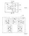
- Fig. 1 shows a block diagram of an integrated circuit IS for differential Data transmission with a high-side driver stage HS and a low-side driver stage LS, whose connections AHS and ALS respectively by a circuit arrangement according to the invention against overvoltage are protected.
- the driver stages LS and HS are each with a transmitter / receiver unit SE, which is used to control the driver stages HS and LS as well as for the evaluation of signals at the connections AHS and ALS serve.
- the integrated circuit IS is connected via a Supply voltage connection VA with a supply voltage from e.g. 5V supplied.
- a reference voltage of e.g. OV is located on one Reference voltage connection BA on.
- Fig. 2 shows a circuit diagram of the low-side driver stage LS of Fig. 1.
- Die Driver stage LS comprises a switching means in the form of an n-channel MOSFET NM, the connection ALS depending on a through the transmitter / receiver unit SE generated drive signal with the Reference potential connects.
- the n-channel MOSFET NM has a substrate Bulk diode SD1 between its drain and reference potential on.
- a Zener diode ZD1 and a diode D1 are connected in series between the terminals ALS and the reference potential looped in, wherein the zener diode ZD1 in the flow direction and the diode D1 connected in the reverse direction are.
- the Zener diode ZD1 and the diode D1 have a substrate diode SD2 or SD3 in the reverse direction between their respective cathode and reference potential.
- the diode D1 prevents a connection of the Zener diode ZD1 in positive Voltages at connection ALS.
- For negative voltages at Terminal ALS operates the diode D1 in the forward direction and the zener diode ZD1 in reverse direction.
- the diode D1 exceeds that of Zener diode ZD1 and diode D1 formed current path and the voltage at the terminal ALS is based on the sum of zener voltage and diode current voltage limited.
- suitable choice of the zener voltage can the voltage threshold until the onset of the clamp mechanism be set.
- a diode D2 which is between the terminal ALS and the drain terminal of the transistor NM is looped in the flow direction prevented at negative terminal voltages a current flow through the Substrate diode SD1 of the n-channel MOSFET.
- the diode D2 has a Substrate diode SD4 between its cathode and reference potential.
- a Zener diode ZD2 which is between the drain terminal of the transistor NM and the reference potential is looped in the reverse direction, is used for Limitation of a positive terminal voltage to a maximum value.
- the Zener diode ZD2 has a substrate diode SD5 between its cathode and reference potential.
- Fig. 3 shows a circuit diagram of the high-side driver stage HS of Fig. 1.
- Die Driver stage HS comprises a switching means in the form of a p-channel MOSFET PM, the connection AHS depending on a through the transmitter / receiver unit SE generated drive signal with the Supply voltage connects.
- the p-channel MOSFET PM has a Substrate or bulk diode SD6 between its drain terminal and its source connection.
- a diode D3 is between the supply voltage and the drain terminal of the transistor PM is looped in the flow direction and has a substrate diode SD7 in the reverse direction between its cathode and the reference potential. It prevents positive connection voltages, which are greater than the supply voltage, a current flow through the substrate diode SD6 of the p-channel MOSFET PM in the supply voltage.
- a zener diode ZD3 which is between the drain terminal of the transistor PM and the reference potential is looped in the reverse direction, is used for Limitation of a positive terminal voltage to a maximum value.
- Zener diode ZD3 has a substrate diode SD8 between its cathode and reference potential.
- the zener diode ZD3 and substrate diode SD6 formed current path conductive and the voltage at the input is based on the sum of zener voltage and Diode supply voltage limited.
- a Zener diode ZD1 ', its associated substrate diode SD2', a diode D1 'and its associated substrate diode SD3' correspond in their Interconnection, function and dimensioning shown in Fig. 2 Components ZD1, SD2, D1 or SD3.
- FIG. 4 shows a diagram of the current-voltage characteristic between the terminals AHS and ALS of Fig. 1.
- the zener diodes are dimensioned such that a clamp mechanism only used at signal amplitudes of greater than ⁇ 45V.
- the input signals become practical not distorted, resulting in safe signal recovery from the Differential signal of the connections AHS and ALS is guaranteed.
- the present invention enables as described above Embodiments will become clear, an effective limitation of positive and negative surges at terminals of an integrated Circuit. Falsifications of a useful signal by clamp mechanisms occur only at very high overvoltages.
- the Circuit arrangement is inexpensive to produce and in a simple manner monolithic integrated, since they are no expensive special components, For example, substrate-free poly elements and no consuming Manufacturing technologies required. It is for example for CAN transceiver, but also for any other integrated transmitter / receiver circuits usable where an overvoltage protection is desired, without external components for surge protection to be realized.
Landscapes
- Emergency Protection Circuit Devices (AREA)
- Semiconductor Integrated Circuits (AREA)
- Logic Circuits (AREA)
- Electronic Switches (AREA)
- Metal-Oxide And Bipolar Metal-Oxide Semiconductor Integrated Circuits (AREA)
Abstract
Description
Die Erfindung bezieht sich auf eine monolithisch integrierbare Schaltungsanordnung zum Überspannungsschutz eines oder mehrerer Anschlüsse einer integrierten Schaltung nach dem Oberbegriff des Anspruchs 1.The invention relates to a monolithically integrable circuit arrangement for overvoltage protection of one or more connections an integrated circuit according to the preamble of the claim 1.
Bei der Handhabung und dem Betrieb integrierter Schaltungen ist darauf zu achten, den Schaltkreis bzw. dessen Anschlüsse oder Anschlusspins vor Überspannungen zu schützen, die eine Störung des regulären Betriebs bzw. eine Beschädigung des Schaltkreises verursachen können. Derartige Überspannungen entstehen beispielsweise durch kapazitive und/oder induktive Kopplung auf gemeinsam geführten Leitungen. So können bei CAN-Bussystemen, deren Busleitung in Kabelbäumen von Kraftfahrzeugen geführt ist, gegenüber einer Substrat- bzw. Bezugsspannung des integrierten Schaltkreises, die das niedrigste Potential des integrierten Schaltkreises darstellt, positive sowie negative Überspannungen mit einer Amplitude von bis zu 45V auftreten. When handling and operating integrated circuits is on it to pay attention to the circuit or its connections or connection pins to protect against surges, which is a disruption of regular operation or damage the circuit. Such overvoltages arise, for example, by capacitive and / or inductive coupling on shared lines. So can be used in CAN bus systems whose bus line in wiring harnesses of Guided motor vehicles, compared to a substrate or reference voltage of the integrated circuit, which has the lowest potential of the integrated circuit represents positive and negative overvoltages with an amplitude of up to 45V.
Eine weitere Ursache von Überspannungen sind sogenannte Electrostatic-Discharge(ESD)-Vorgänge, bei denen energiearme Spannungsspitzen hoher Amplitude entstehen.Another cause of overvoltages is electrostatic discharge (ESD), those with low energy spikes high amplitude arise.
Herkömmliche Schaltungsanordnungen zum Überspannungsschutz integrierter Schaltungen begrenzen Überspannungen, die im Vergleich zur Bezugsspannung positiv sind, auf einen einstellbaren Grenzwert. Wenn die am Anschluss anstehende Spannung den einstellbaren Grenzwert überschreitet, werden Elemente zur Spannungsbegrenzung leitend und begrenzen so die am Anschluss anstehende Spannung. Dieser Mechanismus wird auch als Klemm- oder Clamp-Mechanismus bezeichnet.Conventional integrated circuits for overvoltage protection Circuits limit overvoltages compared to the Reference voltage are positive, to an adjustable limit. If the voltage present at the connection is the adjustable limit value exceeds, voltage limiting elements become conductive and limit the voltage applied to the connection. This mechanism is also referred to as a clamp or clamp mechanism.
Üblicherweise sind die Schaltungsanordnungen zum Überspannungsschutz in die zu schützende integrierte Schaltung monolithisch integriert, da diskrete bzw. externe Bauelemente das Schaltungsdesign erheblich erschweren sowie keine entsprechende Betriebssicherheit gewährleisten können.Usually, the circuit arrangements for overvoltage protection monolithically integrated into the integrated circuit to be protected, because discrete or external components significantly increase the circuit design complicate and ensure no corresponding operational safety can.
Wenn an einem Anschluss im Vergleich zu seiner Substratspannung negative Spannungen anstehen, können parasitäre Box-, Bulk- bzw. Substrat-Dioden in Flussrichtung gepolt werden, wodurch eine Funktionsstörung bzw. Beschädigung der integrierten Schaltung verursacht werden kann. Derartige negative Überspannungen werden herkömmlicherweise auf ein Niveau festgelegt bzw. geklemmt, das um eine Diodendurchflussspannung einer als Spannungsbegrenzungselement dienenden Schutzdiode unter dem Substratpotential liegt, d.h. wenn die am Anschluss anstehende Spannung die Diodendurchflussspannung betragsmäßig überschreitet, wird die Schutzdiode leitend. Die Spannungsgrenzen, an denen ein Clamp-Mechanismus einsetzt, sind folglich für positive und negative Überspannungen bei diesen herkömmlichen Schutzbeschaltungen unterschiedlich. When connected to a terminal compared to its substrate voltage negative voltages can parasitic box, bulk or Substrate diodes are poled in the flow direction, causing a malfunction or damage to the integrated circuit can be. Such negative overvoltages are conventionally set to a level that is clamped by a diode flow voltage one serving as a voltage limiting element Protection diode is below the substrate potential, i. when the am Connection of voltage applied to the diode flow voltage exceeds, the protective diode becomes conductive. The voltage limits, to which a clamping mechanism uses, are therefore for positive and negative overvoltages in these conventional ones Protective circuits different.
Dieser Unterschied kann insbesondere bei einer differentiellen Datenübertragung zu Problemen führen. Bei einer derartigen Datenübertragung werden zwei Datenleitungen benötigt, wobei die Spannungsdifferenz zwischen diesen Datenleitungen zur Kodierung des zu übertragenden Zeichens verwendet wird. Jeweils eine Datenleitung wird an einen zugehörigen Anschluss einer Treiberstufe angeschlossen, wobei die beiden Anschlüsse ein Anschlusspaar bilden. Wenn eine logische "1" übertragen wird, liegt an beiden Anschlüssen das gleiche Potential an. Wenn eine logische "0" übertragen wird, nimmt ein Anschluss ein hohes Potential im Bereich einer Versorgungsspannung und der andere ein niedriges Potential im Bereich der Bezugsspannung an. Diese Art der Datenübertragung ist gegenüber Gleichtaktstörungen auf beiden Leitungen im wesentlichen unempfindlich, sofern die Anschlüsse der Treiberstufe positive und negative Spannungsamplituden zulassen, ohne sie, insbesondere durch einen Clamp-Mechanismus, zu verfälschen.This difference can be especially with a differential data transmission cause problems. In such a data transmission Two data lines are needed, with the voltage difference between these data lines for coding the to be transmitted Character is used. One data line is connected to one associated connection of a driver stage connected, wherein the two connections form a connection pair. If a logical "1" is transmitted, the same potential is applied to both terminals. When a logical "0" is transmitted, a port takes a high Potential in the range of one supply voltage and the other one low potential in the range of the reference voltage. This kind of Data transmission is against common mode interference on both lines essentially insensitive, provided the connections of the driver stage allow positive and negative voltage amplitudes without them, especially through a clamp mechanism, to falsify.
Der Erfindung liegt als technisches Problem die Bereitstellung einer monolithisch integrierbaren Schaltungsanordnung zum Überspannungsschutz der eingangs genannten Art zugrunde, die positive und/oder negative Überspannungen an Anschlüssen einer integrierten Schaltung wirksam begrenzt, Verfälschungen eines Nutzsignals durch Clamp-Mechanismen weitgehend verhindert und kostengünstig ohne Sonderbauelemente herstellbar ist.The invention is a technical problem of providing a monolithic integrable circuit arrangement for overvoltage protection based on the type mentioned, the positive and / or negative Overvoltages on terminals of an integrated circuit effectively limited, distortions of a useful signal by clamp mechanisms largely prevented and inexpensive without special components can be produced.
Die Erfindung löst dieses Problem durch die Bereitstellung einer Schaltungsanordnung mit den Merkmalen des Anspruchs 1 oder 2.The invention solves this problem by providing a circuit arrangement with the features of claim 1 or 2.
Bei der erfindungsgemäßen Schaltungsanordnung nach Anspruch 1 oder 2 sind als Überspannungsschutz eines oder mehrerer Anschlüsse einer Low-Side-Treiberstufe bzw. einer High-Side-Treiberstufe für den Anschluss oder wenigstens einen der Anschlüsse jeweils eine erste Zenerdiode und eine erste Diode vorgesehen, die in Serie zwischen den Anschluss und das Bezugspotential eingeschleift sind, wobei die erste Zenerdiode in Flussrichtung und die erste Diode in Sperrrichtung beschaltet sind.In the circuit arrangement according to claim 1 or 2 are as surge protection of one or more connections a low-side driver stage or a high-side driver stage for the Connection or at least one of the terminals in each case a first Zener diode and a first diode provided in series between the Connection and the reference potential are looped, wherein the first Zener diode in the flow direction and the first diode connected in the reverse direction are.
Die erste Diode verhindert ein Durchschalten der ersten Zenerdiode bei positiven Spannungen am Anschluss. Bei negativen Spannungen am Anschluss arbeitet die erste Diode in Durchlassrichtung und die Zenerdiode in Sperrrichtung. Wenn die negative Spannung am Anschluss die Zenerspannung der ersten Zenerdiode und die Durchflussspannung der ersten Diode überschreitet, wird ein aus der ersten Zenerdiode und der ersten Diode gebildeter Strompfad leitend und die Spannung am Eingang wird auf die Summe aus Zenerspannung und Diodendurchflussspannung begrenzt. Insbesondere nimmt die erste Zenerdiode die Energie negativer ESD-Pulse auf, wodurch eine Zerstörung der Schaltung verhindert wird. Durch geeignete Wahl der Zenerspannung kann die Spannungsschwelle bis zum Einsetzen des Clamp-Mechanismus eingestellt werden.The first diode prevents the first zener diode from being switched on positive voltages at the connection. For negative voltages at Connection operates the first diode in the forward direction and the Zener diode in the reverse direction. If the negative voltage at the connection is the Zener voltage of the first Zener diode and the forward voltage of the exceeds the first diode, one of the first zener diode and the first diode formed current path and the voltage at the input is based on the sum of zener voltage and diode current voltage limited. In particular, the first Zener diode takes the energy negative ESD pulses on, causing a destruction of the circuit is prevented. By a suitable choice of the zener voltage, the Threshold set until the clamp mechanism is inserted become.
Bei der erfindungsgemäßen Schaltungsanordnung nach Anspruch 1 ist als Überspannungsschutz des oder der mehreren Anschlüsse der Low-Side-Treiberstufe, bei der dem jeweiligen Anschluss ein n-Kanal-MOSFET zugeordnet ist, für den Anschluss oder wenigstens einen der Anschlüsse des weiteren eine zweite Diode zwischen diesen Anschluss und einen Anschluss des n-Kanal-MOSFET in Flussrichtung eingeschleift und eine zweite Zenerdiode ist zwischen den Anschluss des n-Kanal-MOSFET und das Bezugspotential in Sperrrichtung eingeschleift.In the circuit arrangement according to the invention according to claim 1 as overvoltage protection of the one or more terminals of the low-side driver stage, at the respective terminal an n-channel MOSFET is assigned, for the connection or at least one of the Connections further a second diode between this terminal and a connection of the n-channel MOSFET in the flow direction looped and a second Zener diode is between the terminal of the n-channel MOSFET and the reference potential looped in the reverse direction.
Die zweite Diode verhindert bei negativen Anschlussspannungen einen Stromfluss durch eine Bulk-Diode des n-Kanal-MOSFET, die dieser zwischen seinem Drain-Anschluß und Bezugspotential aufweist. Die zweite Zenerdiode dient zur Begrenzung einer positiven Anschlussspannung auf einen Maximalwert und dient insbesondere zur Energieaufnahme positiver ESD-Pulse, wodurch eine Zerstörung der Schaltung verhindert wird. Wenn die positive Spannung am Anschluss die Zenerspannung der zweiten Zenerdiode und die Durchflussspannung der zweiten Diode überschreitet, wird ein aus der zweiten Zenerdiode und der zweiten Diode gebildeter Strompfad leitend und die Spannung am Eingang wird auf die Summe aus Zenerspannung und Diodendurchflussspannung begrenzt. Durch geeignete Wahl der Zenerspannung kann die Spannungsschwelle bis zum Einsetzen des Clamp-Mechanismus eingestellt werden.The second diode prevents a negative terminal voltages Current flow through a bulk diode of the n-channel MOSFET, this between its drain terminal and reference potential. The second Zener diode is used to limit a positive terminal voltage to a maximum value and is used in particular for energy absorption positive ESD pulses, which prevents destruction of the circuit becomes. When the positive voltage at the terminal is the Zener voltage the second Zener diode and the forward voltage of the second diode exceeds, one of the second Zener diode and the second diode formed current path and the voltage at the input is on the sum of Zener voltage and diode flow voltage limited. By a suitable choice of the zener voltage, the voltage threshold be adjusted until insertion of the clamp mechanism.
Bei der erfindungsgemäßen Schaltungsanordnung nach Anspruch 2 ist als Überspannungsschutz des oder der mehreren Anschlüsse der High-Side-Treiberstufe, bei der dem jeweiligen Anschluss ein p-Kanal-MOSFET zugeordnet ist, für den Anschluss oder wenigstens einen der Anschlüsse des weiteren eine zweite Diode zwischen die Versorgungsspannung und einen Anschluss des p-Kanal-MOSFET in Flussrichtung eingeschleift und eine zweite Zenerdiode ist zwischen den Anschluss des p-Kanal-MOSFET und das Bezugspotential in Sperrrichtung eingeschleift.In the circuit arrangement according to the invention according to claim 2 as overvoltage protection of the one or more high-side driver stage connections, at the respective terminal a p-channel MOSFET is assigned, for the connection or at least one of the Connections further a second diode between the supply voltage and a connection of the p-channel MOSFET in the flow direction looped in and a second zener diode is between the connector of the p-channel MOSFET and the reference potential in the reverse direction looped.
Die zweite Diode verhindert bei positiven Anschlussspannungen, die größer als die Versorgungsspannung sind, einen Stromfluss durch eine Bulk-Diode des p-Kanal-MOSFET, die dieser zwischen seinem Drain-Anschluß und seinem Source-Anschluss aufweist, in die Versorgungsspannung. Die zweite Zenerdiode dient zur Begrenzung einer positiven Anschlussspannung auf einen Maximalwert und dient insbesondere zur Energieaufnahme positiver ESD-Pulse, wodurch eine Zerstörung der Schaltung verhindert wird. Wenn die positive Spannung am Anschluss die Zenerspannung der zweiten Zenerdiode und die Durchflussspannung der Bulk-Diode überschreitet, wird ein aus der zweiten Zenerdiode und der Bulk-Diode gebildeter Strompfad leitend und die Spannung am Eingang wird auf die Summe aus Zenerspannung und Diodendurchflussspannung begrenzt. Durch geeignete Wahl der Zenerspannung kann die Spannungsschwelle bis zum Einsetzen des Clamp-Mechanismus eingestellt werden.The second diode prevents positive terminal voltages, the are greater than the supply voltage, a current flow through a Bulk diode of the p-channel MOSFET, which this between its drain terminal and its source terminal, into the supply voltage. The second Zener diode is used to limit a positive Terminal voltage to a maximum value and is used in particular for Energy absorption of positive ESD pulses, causing destruction of the Circuit is prevented. When the positive voltage at the terminal the zener voltage of the second Zener diode and the forward voltage exceeds the bulk diode, one of the second zener diode and the bulk diode formed current path conductive and the voltage at Input is to the sum of Zener voltage and diode flow voltage limited. By suitable choice of the zener voltage can the voltage threshold until the onset of the clamp mechanism be set.
In einer Weiterbildung der Erfindung nach Anspruch 3 weist die jeweilige Zenerdiode eine Durchbruchspannung in einem Bereich von 30V bis 50V und/oder die jeweilige Diode eine Durchbruchspannung in einem Bereich von 50V bis 60V auf. Eine derartige Dimensionierung ermöglicht den sicheren Betrieb über einen weiten Spannungsbereich, der gut auf die typischerweise auftretenden Störspannungen angepasst ist.In a development of the invention according to claim 3, the respective Zener diode has a breakdown voltage in a range of 30V up 50V and / or the respective diode a breakdown voltage in one Range from 50V to 60V. Such dimensioning allows safe operation over a wide voltage range, good on the typically occurring interference voltages is adjusted.
In einer Weiterbildung der Erfindung nach Anspruch 4 dient diese zum Überspannungsschutz eines Anschlusses einer Low-Side-Treiberstufe und eines Anschlusses einer High-Side-Treiberstufe, die gemeinsam ein Anschlusspaar zur differentiellen Signalübertragung bilden. Die Schaltungsanordnung ermöglicht einen wirksamen Schutz sowohl vor positiven als auch vor negativen Überspannungen, wobei bei den üblichen Stör- bzw. Überspannungsbeträgen kein Clamp-Mechanismus einsetzt und folglich keine Signalverfälschung auftritt. Dies ermöglicht eine sichere differentielle Signalübertragung auch in gestörten Umgebungen wie beispielsweise im Kraftfahrzeug.In a further development of the invention according to claim 4, this serves for Overvoltage protection of a connection of a low-side driver stage and a port of a high-side driver stage, which together Form terminal pair for differential signal transmission. The circuit arrangement allows effective protection against both positive as well as against negative overvoltages, with the usual Noise or overvoltage amounts do not use a clamp mechanism and consequently no signal corruption occurs. This allows a secure differential signal transmission even in disturbed environments such as for example, in the motor vehicle.
In einer Weiterbildung der Erfindung nach Anspruch 5 dient diese zum Überspannungsschutz einer Sender/Empfänger-Schaltung für ein Bus-System, insbesondere für einen CAN-Bus.In a further development of the invention according to claim 5, this serves for Overvoltage protection of a transmitter / receiver circuit for a bus system, especially for a CAN bus.
Vorteilhafte Ausführungsformen der Erfindung sind in den Zeichnungen dargestellt und werden nachfolgend beschrieben. Hierbei zeigen schematisch:
- Fig. 1
- ein Blockschaltbild einer integrierten Schaltung zur differentiellen Datenübertragung mit einer High-Side-Treiberstufe und einer Low-Side-Treiberstufe, deren Anschlüsse jeweils durch eine erfindungsgemäße Schaltungsanordnung vor Überspannung geschützt sind,
- Fig. 2
- ein Schaltbild der Low-Side-Treiberstufe von Fig. 1 mit Überspannungsschutz,
- Fig. 3
- ein Schaltbild der High-Side-Treiberstufe von Fig. 1 mit Überspannungsschutz und
- Fig. 4
- ein Diagramm der Strom-Spannungs-Kennlinie zwischen den Anschlüssen der Treiberstufen von Fig. 1.
- Fig. 1
- 2 shows a block diagram of an integrated circuit for differential data transmission with a high-side driver stage and a low-side driver stage whose terminals are each protected from overvoltage by a circuit arrangement according to the invention,
- Fig. 2
- 1 is a circuit diagram of the low-side driver stage of FIG. 1 with overvoltage protection;
- Fig. 3
- a circuit diagram of the high-side driver stage of FIG. 1 with overvoltage protection and
- Fig. 4
- a diagram of the current-voltage characteristic between the terminals of the driver stages of Fig. 1st
Fig. 1 zeigt ein Blockschaltbild einer integrierten Schaltung IS zur differentiellen Datenübertragung mit einer High-Side-Treiberstufe HS und einer Low-Side-Treiberstufe LS, deren Anschlüsse AHS und ALS jeweils durch eine erfindungsgemäße Schaltungsanordnung vor Überspannung geschützt sind. Die Treiberstufen LS und HS sind jeweils mit einer Sender/Empfänger-Einheit SE gekoppelt, die zur Ansteuerung der Treiberstufen HS und LS sowie zum Auswerten von Signalen an den Anschlüssen AHS und ALS dient. Die integrierte Schaltung IS wird über einen Versorgungsspannungsanschluss VA mit einer Versorgungsspannung von z.B. 5V versorgt. Eine Bezugsspannung von z.B. OV liegt an einem Bezugsspannungsanschluss BA an.Fig. 1 shows a block diagram of an integrated circuit IS for differential Data transmission with a high-side driver stage HS and a low-side driver stage LS, whose connections AHS and ALS respectively by a circuit arrangement according to the invention against overvoltage are protected. The driver stages LS and HS are each with a transmitter / receiver unit SE, which is used to control the driver stages HS and LS as well as for the evaluation of signals at the connections AHS and ALS serve. The integrated circuit IS is connected via a Supply voltage connection VA with a supply voltage from e.g. 5V supplied. A reference voltage of e.g. OV is located on one Reference voltage connection BA on.
Fig. 2 zeigt ein Schaltbild der Low-Side-Treiberstufe LS von Fig. 1. Die Treiberstufe LS umfasst ein Schaltmittel in Form eines n-Kanal-MOSFET NM, der den Anschluss ALS in Abhängigkeit von einem durch die Sender/Empfänger-Einheit SE erzeugten Ansteuersignal mit dem Bezugspotential verbindet. Der n-Kanal-MOSFET NM weist eine Substrat- bzw. Bulk-Diode SD1 zwischen seinem Drain-Anschluß und Bezugspotential auf. Fig. 2 shows a circuit diagram of the low-side driver stage LS of Fig. 1. Die Driver stage LS comprises a switching means in the form of an n-channel MOSFET NM, the connection ALS depending on a through the transmitter / receiver unit SE generated drive signal with the Reference potential connects. The n-channel MOSFET NM has a substrate Bulk diode SD1 between its drain and reference potential on.
Eine Zenerdiode ZD1 und eine Diode D1 sind in Serie zwischen den Anschluss ALS und das Bezugspotential eingeschleift, wobei die Zenerdiode ZD1 in Flussrichtung und die Diode D1 in Sperrrichtung beschaltet sind. Die Zenerdiode ZD1 sowie die Diode D1 weisen eine Substrat-Diode SD2 bzw. SD3 in Sperrrichtung zwischen ihrer jeweiligen Kathode und Bezugspotential auf.A Zener diode ZD1 and a diode D1 are connected in series between the terminals ALS and the reference potential looped in, wherein the zener diode ZD1 in the flow direction and the diode D1 connected in the reverse direction are. The Zener diode ZD1 and the diode D1 have a substrate diode SD2 or SD3 in the reverse direction between their respective cathode and reference potential.
Die Diode D1 verhindert ein Durchschalten der Zenerdiode ZD1 bei positiven Spannungen am Anschluss ALS. Bei negativen Spannungen am Anschluss ALS arbeitet die Diode D1 in Durchlassrichtung und die Zenerdiode ZD1 in Sperrrichtung. Wenn die negative Spannung am Anschluss ALS die Zenerspannung der Zenerdiode ZD1 und die Durchflussspannung der Diode D1 überschreitet, wird der aus Zenerdiode ZD1 und Diode D1 gebildete Strompfad leitend und die Spannung am Anschluss ALS wird auf die Summe aus Zenerspannung und Diodendurchflussspannung begrenzt. Durch geeignete Wahl der Zenerspannung kann die Spannungsschwelle bis zum Einsetzen des Clamp-Mechanismus eingestellt werden.The diode D1 prevents a connection of the Zener diode ZD1 in positive Voltages at connection ALS. For negative voltages at Terminal ALS operates the diode D1 in the forward direction and the zener diode ZD1 in reverse direction. When the negative voltage at the terminal AS the zener voltage of Zener diode ZD1 and the forward voltage the diode D1 exceeds that of Zener diode ZD1 and diode D1 formed current path and the voltage at the terminal ALS is based on the sum of zener voltage and diode current voltage limited. By suitable choice of the zener voltage can the voltage threshold until the onset of the clamp mechanism be set.
Eine Diode D2, die zwischen den Anschluss ALS und den Drain-Anschluß des Transistors NM in Flussrichtung eingeschleift ist, verhindert bei negativen Anschlussspannungen einen Stromfluss durch die Substrat-Diode SD1 des n-Kanal-MOSFET. Die Diode D2 weist eine Substrat-Diode SD4 zwischen ihrer Kathode und Bezugspotential auf.A diode D2, which is between the terminal ALS and the drain terminal of the transistor NM is looped in the flow direction prevented at negative terminal voltages a current flow through the Substrate diode SD1 of the n-channel MOSFET. The diode D2 has a Substrate diode SD4 between its cathode and reference potential.
Eine Zenerdiode ZD2, die zwischen den Drain-Anschluß des Transistors NM und das Bezugspotential in Sperrrichtung eingeschleift ist, dient zur Begrenzung einer positiven Anschlussspannung auf einen Maximalwert. Die Zenerdiode ZD2 weist eine Substrat-Diode SD5 zwischen ihrer Kathode und Bezugspotential auf. Wenn die positive Spannung am Anschluss ALS die Zenerspannung der Zenerdiode ZD2 und die Durchflussspannung der Diode D2 überschreitet, wird der aus der Zenerdiode ZD2 und der Diode D2 gebildete Strompfad leitend und die Spannung am Anschluss ALS wird auf die Summe aus Zenerspannung und Diodendurchflussspannung begrenzt. Durch geeignete Wahl der Zenerspannung kann die Spannungsschwelle bis zum Einsetzen des Clamp-Mechanismus eingestellt werden.A Zener diode ZD2, which is between the drain terminal of the transistor NM and the reference potential is looped in the reverse direction, is used for Limitation of a positive terminal voltage to a maximum value. The Zener diode ZD2 has a substrate diode SD5 between its cathode and reference potential. When the positive voltage at the terminal AS the zener voltage of the zener diode ZD2 and the forward voltage the diode exceeds D2, the from the Zener diode ZD2 and the diode D2 formed current path conductive and the voltage at terminal ALS is set to the sum of zener voltage and diode current voltage limited. By suitable choice of the zener voltage can the voltage threshold until the onset of Clamp mechanism can be adjusted.
Fig. 3 zeigt ein Schaltbild der High-Side-Treiberstufe HS von Fig. 1. Die Treiberstufe HS umfasst ein Schaltmittel in Form eines p-Kanal-MOSFET PM, der den Anschluss AHS in Abhängigkeit von einem durch die Sender/Empfänger-Einheit SE erzeugten Ansteuersignal mit der Versorgungsspannung verbindet. Der p-Kanal-MOSFET PM weist eine Substrat- bzw. Bulk-Diode SD6 zwischen seinem Drain-Anschluss und seinem Source-Anschluss auf.Fig. 3 shows a circuit diagram of the high-side driver stage HS of Fig. 1. Die Driver stage HS comprises a switching means in the form of a p-channel MOSFET PM, the connection AHS depending on a through the transmitter / receiver unit SE generated drive signal with the Supply voltage connects. The p-channel MOSFET PM has a Substrate or bulk diode SD6 between its drain terminal and its source connection.
Eine Diode D3 ist zwischen die Versorgungsspannung und den Drain-Anschluß des Transistors PM in Flussrichtung eingeschleift und weist eine Substrat-Diode SD7 in Sperrrichtung zwischen ihrer Kathode und dem Bezugspotential auf. Sie verhindert bei positiven Anschlussspannungen, die größer als die Versorgungsspannung sind, einen Stromfluss durch die Substrat-Diode SD6 des p-Kanal-MOSFET PM in die Versorgungsspannung.A diode D3 is between the supply voltage and the drain terminal of the transistor PM is looped in the flow direction and has a substrate diode SD7 in the reverse direction between its cathode and the reference potential. It prevents positive connection voltages, which are greater than the supply voltage, a current flow through the substrate diode SD6 of the p-channel MOSFET PM in the supply voltage.
Eine Zenerdiode ZD3, die zwischen den Drain-Anschluß des Transistors PM und das Bezugspotential in Sperrrichtung eingeschleift ist, dient zur Begrenzung einer positiven Anschlussspannung auf einen Maximalwert. Die Zenerdiode ZD3 weist eine Substrat-Diode SD8 zwischen ihrer Kathode und Bezugspotential auf. Wenn die positive Spannung am Anschluss AHS die Zenerspannung der Zenerdiode ZD3 und die Durchflussspannung der Substrat-Diode SD6 überschreitet, wird der aus Zenerdiode ZD3 und Substrat-Diode SD6 gebildete Strompfad leitend und die Spannung am Eingang wird auf die Summe aus Zenerspannung und Diodendurchflussspannung begrenzt. Durch geeignete Wahl der Zenerspannung kann die Spannungsschwelle bis zum Einsetzen des Clamp-Mechanismus eingestellt werden.A zener diode ZD3, which is between the drain terminal of the transistor PM and the reference potential is looped in the reverse direction, is used for Limitation of a positive terminal voltage to a maximum value. Zener diode ZD3 has a substrate diode SD8 between its cathode and reference potential. When the positive voltage at the terminal AHS the zener voltage of the Zener diode ZD3 and the forward voltage exceeds the substrate diode SD6, the zener diode ZD3 and substrate diode SD6 formed current path conductive and the voltage at the input is based on the sum of zener voltage and Diode supply voltage limited. By suitable choice of the zener voltage can the voltage threshold until the onset of Clamp mechanism can be adjusted.
Eine Zenerdiode ZD1', ihre zugehörige Substrat-Diode SD2', eine Diode D1' sowie ihre zugehörige Substrat-Diode SD3' entsprechen in ihrer Verschaltung, Funktion und Dimensionierung den in Fig. 2 gezeigten Bauelementen ZD1, SD2, D1 bzw. SD3.A Zener diode ZD1 ', its associated substrate diode SD2', a diode D1 'and its associated substrate diode SD3' correspond in their Interconnection, function and dimensioning shown in Fig. 2 Components ZD1, SD2, D1 or SD3.
Fig. 4 zeigt ein Diagramm der Strom-Spannungs-Kennlinie zwischen den Anschlüssen AHS und ALS von Fig. 1. Wie aus dem Diagramm ersichtlich ist, sind die Zenerdioden derart dimensioniert, dass ein Clamp-Mechanismus erst bei Signalamplituden von größer als ±45V einsetzt. Bei kleineren Signalamplituden werden die Eingangssignale praktisch nicht verfälscht, wodurch eine sichere Signalrückgewinnung aus dem Differenzsignal der Anschlüsse AHS und ALS gewährleistet ist.4 shows a diagram of the current-voltage characteristic between the terminals AHS and ALS of Fig. 1. As seen from the diagram is, the zener diodes are dimensioned such that a clamp mechanism only used at signal amplitudes of greater than ± 45V. At lower signal amplitudes, the input signals become practical not distorted, resulting in safe signal recovery from the Differential signal of the connections AHS and ALS is guaranteed.
Die vorliegende Erfindung ermöglicht, wie aus den oben beschriebenen Ausführungsbeispielen deutlich wird, eine wirksame Begrenzung von positiven und negativen Überspannungen an Anschlüssen einer integrierten Schaltung. Verfälschungen eines Nutzsignals durch Clamp-Mechanismen treten erst bei sehr hohen Überspannungen auf. Die Schaltungsanordnung ist kostengünstig herstellbar und in einfache Weise monolithisch integrierbar, da sie keine teuren Sonderbauelemente, beispielsweise substratfreie Poly-Elemente und keine aufwendigen Herstellungs-Technologien erfordert. Sie ist beispielsweise für CAN-Transceiver, aber auch für beliebige andere integrierte Sender/Empfänger-Schaltungen verwendbar, bei denen ein Überspannungsschutz gewünscht wird, der ohne externe Bauelemente zum Überspannungsschutz realisiert werden soll.The present invention enables as described above Embodiments will become clear, an effective limitation of positive and negative surges at terminals of an integrated Circuit. Falsifications of a useful signal by clamp mechanisms occur only at very high overvoltages. The Circuit arrangement is inexpensive to produce and in a simple manner monolithic integrated, since they are no expensive special components, For example, substrate-free poly elements and no consuming Manufacturing technologies required. It is for example for CAN transceiver, but also for any other integrated transmitter / receiver circuits usable where an overvoltage protection is desired, without external components for surge protection to be realized.
Claims (5)
dadurch gekennzeichnet, dass
für den Anschluss oder wenigstens einen der Anschlüsse (ALS) jeweils eine erste Zenerdiode (ZD1) und eine erste Diode (D1) vorgesehen sind, die in Serie zwischen den Anschluss (ALS) und das Bezugspotential eingeschleift sind, wobei die erste Zenerdiode (ZD1) in Flussrichtung und die erste Diode (D1) in Sperrrichtung beschaltet sind, eine zweite Diode (D2) zwischen diesen Anschluss (ALS) und einen Anschluss des n-Kanal-MOSFET in Flussrichtung eingeschleift ist und eine zweite Zenerdiode (ZD2) zwischen diesen Anschluss des n-Kanal-MOSFET und das Bezugspotential in Sperrrichtung eingeschleift ist.Monolithically integrable circuit arrangement for overvoltage protection of one or more terminals (ALS) of a low-side driver stage (LS) of an integrated circuit (IS), in which the respective terminal (ALS) is associated with an n-channel MOSFET (NM), the Connection (ALS) in response to a drive signal to a reference potential of the integrated circuit (IS) connects,
characterized in that
a first Zener diode (ZD1) and a first diode (D1) are provided for the connection or at least one of the terminals (ALS), which are connected in series between the terminal (ALS) and the reference potential, the first Zener diode (ZD1) in the flow direction and the first diode (D1) are reverse-connected, a second diode (D2) between this terminal (ALS) and a terminal of the n-channel MOSFET in the flow direction is looped and a second Zener diode (ZD2) between this terminal of the n-channel MOSFET and the reference potential is looped in the reverse direction.
dadurch gekennzeichnet, dass
für den Anschluss oder wenigstens einen der Anschlüsse (AHS) jeweils eine erste Zenerdiode (ZD1') und eine erste Diode (D1') vorgesehen sind, die in Serie zwischen den Anschluss (AHS) und das Bezugspotential eingeschleift sind, wobei die erste Zenerdiode (ZD1') in Flussrichtung und die erste Diode (D1') in Sperrrichtung beschaltet sind, eine zweite Diode (D3) zwischen die Versorgungsspannung und einen Anschluss des p-Kanal-MOSFET (PM) in Flussrichtung eingeschleift ist und eine zweite Zenerdiode (ZD3) zwischen den Anschluss des p-Kanal-MOSFET und das Bezugspotential in Sperrrichtung eingeschleift ist.Monolithically integrable circuit arrangement for overvoltage protection of one or more terminals (AHS) of a high-side driver stage (HS) of an integrated circuit (IS), in which the respective terminal (AHS) is associated with a p-channel MOSFET (PM), the Connection (AHS) in dependence on a drive signal with a supply voltage of the integrated circuit (IS) connects,
characterized in that
a first Zener diode (ZD1 ') and a first diode (D1') are provided for the connection or at least one of the connections (AHS), which are connected in series between the connection (AHS) and the reference potential, the first Zener diode (AHS) ZD1 ') in the flow direction and the first diode (D1') are connected in the reverse direction, a second diode (D3) between the supply voltage and a terminal of the p-channel MOSFET (PM) is inserted in the flow direction and a second Zener diode (ZD3) is connected between the terminal of the p-channel MOSFET and the reference potential in the reverse direction.
Applications Claiming Priority (2)
| Application Number | Priority Date | Filing Date | Title |
|---|---|---|---|
| DE10335383A DE10335383A1 (en) | 2003-07-28 | 2003-07-28 | Monolithically integrated circuit arrangement for overvoltage protection |
| DE10335383 | 2003-07-28 |
Publications (2)
| Publication Number | Publication Date |
|---|---|
| EP1503473A1 true EP1503473A1 (en) | 2005-02-02 |
| EP1503473B1 EP1503473B1 (en) | 2009-07-01 |
Family
ID=33521533
Family Applications (1)
| Application Number | Title | Priority Date | Filing Date |
|---|---|---|---|
| EP04017574A Expired - Lifetime EP1503473B1 (en) | 2003-07-28 | 2004-07-24 | Monolithically integrated circuit for overvoltage protection |
Country Status (3)
| Country | Link |
|---|---|
| US (1) | US7130175B2 (en) |
| EP (1) | EP1503473B1 (en) |
| DE (2) | DE10335383A1 (en) |
Families Citing this family (6)
| Publication number | Priority date | Publication date | Assignee | Title |
|---|---|---|---|---|
| DE10251473B3 (en) * | 2002-11-05 | 2004-06-17 | Siemens Ag | Protection circuit for protection against overvoltage for a CAN bus transceiver |
| DE102006021747A1 (en) * | 2006-05-10 | 2007-11-15 | Robert Bosch Gmbh | protection circuit |
| US8116057B2 (en) * | 2006-12-21 | 2012-02-14 | Apple Inc. | Data port transient protection apparatus and methods |
| US8699189B2 (en) | 2012-05-22 | 2014-04-15 | Honeywell International Inc. | High precision clipping regulator circuit |
| DE102021203501A1 (en) | 2021-04-09 | 2022-10-13 | Robert Bosch Gesellschaft mit beschränkter Haftung | Protection circuit for CAN transceiver |
| DE102024123189A1 (en) * | 2024-08-14 | 2026-02-19 | Hanon Systems Efp Deutschland Gmbh | CONTROL DEVICE FOR A CONSUMER IN A VEHICLE; CONTROL SYSTEM AND VEHICLE |
Citations (3)
| Publication number | Priority date | Publication date | Assignee | Title |
|---|---|---|---|---|
| US5448180A (en) | 1991-03-16 | 1995-09-05 | Robert Bosch Gmbh | Transmitter end stage |
| US5986862A (en) * | 1996-12-31 | 1999-11-16 | Lg Semicon Co., Ltd. | Electrostatic discharge protection circuit |
| EP1178531A1 (en) * | 2000-08-05 | 2002-02-06 | Philips Corporate Intellectual Property GmbH | Input protecting circuit in use with a CMOS semiconductor device |
Family Cites Families (6)
| Publication number | Priority date | Publication date | Assignee | Title |
|---|---|---|---|---|
| NL7614118A (en) * | 1976-12-20 | 1978-06-22 | Philips Nv | CIRCUIT FOR PROTECTING TELEPHONE LINES. |
| DE4407279C1 (en) * | 1994-03-04 | 1994-10-13 | Siemens Ag | Semiconductor component for the overvoltage protection of MOSFETs and IGBTs |
| EP0773588B1 (en) * | 1995-11-10 | 2002-06-19 | Consorzio per la Ricerca sulla Microelettronica nel Mezzogiorno - CoRiMMe | MOS integrated device comprising a gate protection diode |
| JPH10189761A (en) * | 1996-12-20 | 1998-07-21 | Fuji Electric Co Ltd | Semiconductor device |
| DE69941977D1 (en) * | 1999-06-01 | 2010-03-18 | Imec | ESD protection component for medium trigger voltage |
| DE10233220B3 (en) * | 2002-07-22 | 2004-05-19 | Texas Instruments Deutschland Gmbh | Comparator with hysteresis |
-
2003
- 2003-07-28 DE DE10335383A patent/DE10335383A1/en not_active Withdrawn
-
2004
- 2004-07-24 DE DE502004009683T patent/DE502004009683D1/en not_active Expired - Lifetime
- 2004-07-24 EP EP04017574A patent/EP1503473B1/en not_active Expired - Lifetime
- 2004-07-27 US US10/900,643 patent/US7130175B2/en not_active Expired - Lifetime
Patent Citations (3)
| Publication number | Priority date | Publication date | Assignee | Title |
|---|---|---|---|---|
| US5448180A (en) | 1991-03-16 | 1995-09-05 | Robert Bosch Gmbh | Transmitter end stage |
| US5986862A (en) * | 1996-12-31 | 1999-11-16 | Lg Semicon Co., Ltd. | Electrostatic discharge protection circuit |
| EP1178531A1 (en) * | 2000-08-05 | 2002-02-06 | Philips Corporate Intellectual Property GmbH | Input protecting circuit in use with a CMOS semiconductor device |
Also Published As
| Publication number | Publication date |
|---|---|
| EP1503473B1 (en) | 2009-07-01 |
| DE10335383A1 (en) | 2005-02-24 |
| US7130175B2 (en) | 2006-10-31 |
| DE502004009683D1 (en) | 2009-08-13 |
| US20050024801A1 (en) | 2005-02-03 |
Similar Documents
| Publication | Publication Date | Title |
|---|---|---|
| EP0576444B1 (en) | Monolithic integrated transmitter end stage | |
| DE102009061073B4 (en) | Semiconductor device with impedance control circuit | |
| WO1990009713A1 (en) | Network interface | |
| DE19728783A1 (en) | Overvoltage protection circuit for inputs to integrated circuits | |
| DE102005043907B4 (en) | Semiconductor circuits and transmission devices for fail-safe communication in motor vehicles | |
| DE102007053089B4 (en) | Electrical and electronic system | |
| EP1503473B1 (en) | Monolithically integrated circuit for overvoltage protection | |
| DE102020104869B3 (en) | CIRCUIT ARRANGEMENT WITH GALVANIC ISOLATION | |
| DE102007018237A1 (en) | Circuit with improved ESD protection with repetitive pulse loading | |
| EP0495142B1 (en) | Protection against inverted polarity and overvoltage for circuit arrangements | |
| DE4428115C2 (en) | Control unit with a circuit arrangement for protecting the control unit when the control unit mass is interrupted | |
| DE10349092A1 (en) | Integrated circuit arrangement for detecting and outputting control signals | |
| DE102004055057A1 (en) | Protection for integrated sensor circuit output from overvoltage, reverse polarity and supply line faults, includes semiconductor switch operating in accordance with limiting potentials | |
| EP1966866A2 (en) | Circuit arrangement featuring explosion protection | |
| DE2644401B1 (en) | Electronic switch | |
| EP0643515A2 (en) | Arrangement for bidirectional transmission of data | |
| DE102006021847A1 (en) | Circuit arrangement for protection against electrostatic discharges and method for discharging electrostatic discharges | |
| DE10200518B4 (en) | Voltage limiter for the interface circuit of a communication bus | |
| EP3788654B1 (en) | Protection circuit against electrostatic discharges | |
| DE69601198T2 (en) | Short-circuit protection for an audio-video data bus | |
| DE10007607B4 (en) | Fail-safe overvoltage protection circuit | |
| DE19633723C1 (en) | Level conversion circuit for combined CMOS and ECL circuit | |
| EP0766399B1 (en) | Bidirectional driver circuit for PCI bussystem | |
| DE4222279C1 (en) | Arrangement for the transmission of signals | |
| DE10223169B4 (en) | Circuit arrangement for frequency division |
Legal Events
| Date | Code | Title | Description |
|---|---|---|---|
| PUAI | Public reference made under article 153(3) epc to a published international application that has entered the european phase |
Free format text: ORIGINAL CODE: 0009012 |
|
| AK | Designated contracting states |
Kind code of ref document: A1 Designated state(s): AT BE BG CH CY CZ DE DK EE ES FI FR GB GR HU IE IT LI LU MC NL PL PT RO SE SI SK TR |
|
| AX | Request for extension of the european patent |
Extension state: AL HR LT LV MK |
|
| 17P | Request for examination filed |
Effective date: 20050111 |
|
| AKX | Designation fees paid |
Designated state(s): DE FR GB |
|
| 17Q | First examination report despatched |
Effective date: 20070326 |
|
| GRAP | Despatch of communication of intention to grant a patent |
Free format text: ORIGINAL CODE: EPIDOSNIGR1 |
|
| RTI1 | Title (correction) |
Free format text: MONOLITHICALLY INTEGRATED CIRCUIT FOR OVERVOLTAGE PROTECTION |
|
| GRAS | Grant fee paid |
Free format text: ORIGINAL CODE: EPIDOSNIGR3 |
|
| GRAA | (expected) grant |
Free format text: ORIGINAL CODE: 0009210 |
|
| AK | Designated contracting states |
Kind code of ref document: B1 Designated state(s): DE FR GB |
|
| REG | Reference to a national code |
Ref country code: GB Ref legal event code: FG4D Free format text: NOT ENGLISH |
|
| REF | Corresponds to: |
Ref document number: 502004009683 Country of ref document: DE Date of ref document: 20090813 Kind code of ref document: P |
|
| RAP2 | Party data changed (patent owner data changed or rights of a patent transferred) |
Owner name: ATMEL AUTOMOTIVE GMBH |
|
| PLBE | No opposition filed within time limit |
Free format text: ORIGINAL CODE: 0009261 |
|
| STAA | Information on the status of an ep patent application or granted ep patent |
Free format text: STATUS: NO OPPOSITION FILED WITHIN TIME LIMIT |
|
| 26N | No opposition filed |
Effective date: 20100406 |
|
| PG25 | Lapsed in a contracting state [announced via postgrant information from national office to epo] |
Ref country code: FR Free format text: LAPSE BECAUSE OF NON-PAYMENT OF DUE FEES Effective date: 20090901 |
|
| REG | Reference to a national code |
Ref country code: FR Ref legal event code: ST Effective date: 20100930 |
|
| PG25 | Lapsed in a contracting state [announced via postgrant information from national office to epo] |
Ref country code: GB Free format text: LAPSE BECAUSE OF NON-PAYMENT OF DUE FEES Effective date: 20091001 |
|
| REG | Reference to a national code |
Ref country code: DE Ref legal event code: R082 Ref document number: 502004009683 Country of ref document: DE Representative=s name: GRUENECKER, KINKELDEY, STOCKMAIR & SCHWANHAEUS, DE Effective date: 20130529 Ref country code: DE Ref legal event code: R081 Ref document number: 502004009683 Country of ref document: DE Owner name: ATMEL CORP., US Free format text: FORMER OWNER: ATMEL AUTOMOTIVE GMBH, 74072 HEILBRONN, DE Effective date: 20130529 Ref country code: DE Ref legal event code: R081 Ref document number: 502004009683 Country of ref document: DE Owner name: ATMEL CORP., SAN JOSE, US Free format text: FORMER OWNER: ATMEL AUTOMOTIVE GMBH, 74072 HEILBRONN, DE Effective date: 20130529 Ref country code: DE Ref legal event code: R082 Ref document number: 502004009683 Country of ref document: DE Representative=s name: GRUENECKER PATENT- UND RECHTSANWAELTE PARTG MB, DE Effective date: 20130529 |
|
| P01 | Opt-out of the competence of the unified patent court (upc) registered |
Effective date: 20230528 |
|
| PGFP | Annual fee paid to national office [announced via postgrant information from national office to epo] |
Ref country code: DE Payment date: 20230620 Year of fee payment: 20 |
|
| REG | Reference to a national code |
Ref country code: DE Ref legal event code: R071 Ref document number: 502004009683 Country of ref document: DE |