EP1504923A2 - Document de valeur et la méthode de sa production - Google Patents
Document de valeur et la méthode de sa production Download PDFInfo
- Publication number
- EP1504923A2 EP1504923A2 EP04254688A EP04254688A EP1504923A2 EP 1504923 A2 EP1504923 A2 EP 1504923A2 EP 04254688 A EP04254688 A EP 04254688A EP 04254688 A EP04254688 A EP 04254688A EP 1504923 A2 EP1504923 A2 EP 1504923A2
- Authority
- EP
- European Patent Office
- Prior art keywords
- document
- security device
- value according
- layer
- oxide
- Prior art date
- Legal status (The legal status is an assumption and is not a legal conclusion. Google has not performed a legal analysis and makes no representation as to the accuracy of the status listed.)
- Granted
Links
- 238000004519 manufacturing process Methods 0.000 title claims abstract description 24
- 239000000758 substrate Substances 0.000 claims abstract description 27
- 239000010409 thin film Substances 0.000 claims abstract description 17
- 239000011248 coating agent Substances 0.000 claims abstract description 15
- 238000000576 coating method Methods 0.000 claims abstract description 15
- 239000000463 material Substances 0.000 claims abstract description 13
- 229910052751 metal Inorganic materials 0.000 claims abstract description 6
- 239000002184 metal Substances 0.000 claims abstract description 6
- 238000010348 incorporation Methods 0.000 claims abstract description 5
- VYPSYNLAJGMNEJ-UHFFFAOYSA-N Silicium dioxide Chemical compound O=[Si]=O VYPSYNLAJGMNEJ-UHFFFAOYSA-N 0.000 claims description 16
- 239000006096 absorbing agent Substances 0.000 claims description 13
- 229910052782 aluminium Inorganic materials 0.000 claims description 12
- XAGFODPZIPBFFR-UHFFFAOYSA-N aluminium Chemical group [Al] XAGFODPZIPBFFR-UHFFFAOYSA-N 0.000 claims description 12
- PXHVJJICTQNCMI-UHFFFAOYSA-N Nickel Chemical compound [Ni] PXHVJJICTQNCMI-UHFFFAOYSA-N 0.000 claims description 11
- 230000003287 optical effect Effects 0.000 claims description 11
- OKTJSMMVPCPJKN-UHFFFAOYSA-N Carbon Chemical compound [C] OKTJSMMVPCPJKN-UHFFFAOYSA-N 0.000 claims description 10
- XEEYBQQBJWHFJM-UHFFFAOYSA-N Iron Chemical compound [Fe] XEEYBQQBJWHFJM-UHFFFAOYSA-N 0.000 claims description 10
- 238000000034 method Methods 0.000 claims description 10
- KDLHZDBZIXYQEI-UHFFFAOYSA-N Palladium Chemical compound [Pd] KDLHZDBZIXYQEI-UHFFFAOYSA-N 0.000 claims description 8
- BASFCYQUMIYNBI-UHFFFAOYSA-N platinum Chemical compound [Pt] BASFCYQUMIYNBI-UHFFFAOYSA-N 0.000 claims description 8
- 239000000377 silicon dioxide Substances 0.000 claims description 8
- 239000011651 chromium Substances 0.000 claims description 7
- 229910045601 alloy Inorganic materials 0.000 claims description 6
- 239000000956 alloy Substances 0.000 claims description 6
- 229910052799 carbon Inorganic materials 0.000 claims description 6
- -1 hafnium nitride Chemical class 0.000 claims description 6
- VYZAMTAEIAYCRO-UHFFFAOYSA-N Chromium Chemical compound [Cr] VYZAMTAEIAYCRO-UHFFFAOYSA-N 0.000 claims description 4
- RYGMFSIKBFXOCR-UHFFFAOYSA-N Copper Chemical compound [Cu] RYGMFSIKBFXOCR-UHFFFAOYSA-N 0.000 claims description 4
- ZOKXTWBITQBERF-UHFFFAOYSA-N Molybdenum Chemical compound [Mo] ZOKXTWBITQBERF-UHFFFAOYSA-N 0.000 claims description 4
- XUIMIQQOPSSXEZ-UHFFFAOYSA-N Silicon Chemical compound [Si] XUIMIQQOPSSXEZ-UHFFFAOYSA-N 0.000 claims description 4
- BQCADISMDOOEFD-UHFFFAOYSA-N Silver Chemical compound [Ag] BQCADISMDOOEFD-UHFFFAOYSA-N 0.000 claims description 4
- ATJFFYVFTNAWJD-UHFFFAOYSA-N Tin Chemical compound [Sn] ATJFFYVFTNAWJD-UHFFFAOYSA-N 0.000 claims description 4
- GWEVSGVZZGPLCZ-UHFFFAOYSA-N Titan oxide Chemical compound O=[Ti]=O GWEVSGVZZGPLCZ-UHFFFAOYSA-N 0.000 claims description 4
- RTAQQCXQSZGOHL-UHFFFAOYSA-N Titanium Chemical compound [Ti] RTAQQCXQSZGOHL-UHFFFAOYSA-N 0.000 claims description 4
- XLOMVQKBTHCTTD-UHFFFAOYSA-N Zinc monoxide Chemical compound [Zn]=O XLOMVQKBTHCTTD-UHFFFAOYSA-N 0.000 claims description 4
- ADCOVFLJGNWWNZ-UHFFFAOYSA-N antimony trioxide Chemical compound O=[Sb]O[Sb]=O ADCOVFLJGNWWNZ-UHFFFAOYSA-N 0.000 claims description 4
- 229910052804 chromium Inorganic materials 0.000 claims description 4
- 229910017052 cobalt Inorganic materials 0.000 claims description 4
- 239000010941 cobalt Substances 0.000 claims description 4
- GUTLYIVDDKVIGB-UHFFFAOYSA-N cobalt atom Chemical compound [Co] GUTLYIVDDKVIGB-UHFFFAOYSA-N 0.000 claims description 4
- 150000001875 compounds Chemical class 0.000 claims description 4
- 229910052802 copper Inorganic materials 0.000 claims description 4
- 239000010949 copper Substances 0.000 claims description 4
- 229910052732 germanium Inorganic materials 0.000 claims description 4
- GNPVGFCGXDBREM-UHFFFAOYSA-N germanium atom Chemical compound [Ge] GNPVGFCGXDBREM-UHFFFAOYSA-N 0.000 claims description 4
- 229910002804 graphite Inorganic materials 0.000 claims description 4
- 239000010439 graphite Substances 0.000 claims description 4
- 229910052742 iron Inorganic materials 0.000 claims description 4
- MRELNEQAGSRDBK-UHFFFAOYSA-N lanthanum(3+);oxygen(2-) Chemical compound [O-2].[O-2].[O-2].[La+3].[La+3] MRELNEQAGSRDBK-UHFFFAOYSA-N 0.000 claims description 4
- 239000000203 mixture Substances 0.000 claims description 4
- 229910052750 molybdenum Inorganic materials 0.000 claims description 4
- 239000011733 molybdenum Substances 0.000 claims description 4
- PLDDOISOJJCEMH-UHFFFAOYSA-N neodymium(3+);oxygen(2-) Chemical compound [O-2].[O-2].[O-2].[Nd+3].[Nd+3] PLDDOISOJJCEMH-UHFFFAOYSA-N 0.000 claims description 4
- 229910052759 nickel Inorganic materials 0.000 claims description 4
- RVTZCBVAJQQJTK-UHFFFAOYSA-N oxygen(2-);zirconium(4+) Chemical compound [O-2].[O-2].[Zr+4] RVTZCBVAJQQJTK-UHFFFAOYSA-N 0.000 claims description 4
- 229910052763 palladium Inorganic materials 0.000 claims description 4
- 229910052697 platinum Inorganic materials 0.000 claims description 4
- 229910052703 rhodium Inorganic materials 0.000 claims description 4
- 239000010948 rhodium Substances 0.000 claims description 4
- MHOVAHRLVXNVSD-UHFFFAOYSA-N rhodium atom Chemical compound [Rh] MHOVAHRLVXNVSD-UHFFFAOYSA-N 0.000 claims description 4
- 229910052710 silicon Inorganic materials 0.000 claims description 4
- 239000010703 silicon Substances 0.000 claims description 4
- LIVNPJMFVYWSIS-UHFFFAOYSA-N silicon monoxide Chemical compound [Si-]#[O+] LIVNPJMFVYWSIS-UHFFFAOYSA-N 0.000 claims description 4
- 229910052709 silver Inorganic materials 0.000 claims description 4
- 239000004332 silver Substances 0.000 claims description 4
- 239000011135 tin Substances 0.000 claims description 4
- 229910052718 tin Inorganic materials 0.000 claims description 4
- 229910052719 titanium Inorganic materials 0.000 claims description 4
- 239000010936 titanium Substances 0.000 claims description 4
- WFKWXMTUELFFGS-UHFFFAOYSA-N tungsten Chemical compound [W] WFKWXMTUELFFGS-UHFFFAOYSA-N 0.000 claims description 4
- 229910052721 tungsten Inorganic materials 0.000 claims description 4
- 239000010937 tungsten Substances 0.000 claims description 4
- ZNOKGRXACCSDPY-UHFFFAOYSA-N tungsten trioxide Chemical compound O=[W](=O)=O ZNOKGRXACCSDPY-UHFFFAOYSA-N 0.000 claims description 4
- 229910052720 vanadium Inorganic materials 0.000 claims description 4
- GPPXJZIENCGNKB-UHFFFAOYSA-N vanadium Chemical compound [V]#[V] GPPXJZIENCGNKB-UHFFFAOYSA-N 0.000 claims description 4
- 239000004922 lacquer Substances 0.000 claims description 3
- 229920003023 plastic Polymers 0.000 claims description 3
- 239000004033 plastic Substances 0.000 claims description 3
- 235000012239 silicon dioxide Nutrition 0.000 claims description 3
- VFLXBUJKRRJAKY-UHFFFAOYSA-N 13768-86-0 Chemical compound O=[Se](=O)=O VFLXBUJKRRJAKY-UHFFFAOYSA-N 0.000 claims description 2
- 239000005083 Zinc sulfide Substances 0.000 claims description 2
- MCMNRKCIXSYSNV-UHFFFAOYSA-N ZrO2 Inorganic materials O=[Zr]=O MCMNRKCIXSYSNV-UHFFFAOYSA-N 0.000 claims description 2
- 150000001252 acrylic acid derivatives Chemical class 0.000 claims description 2
- 229910000420 cerium oxide Inorganic materials 0.000 claims description 2
- 229910001940 europium oxide Inorganic materials 0.000 claims description 2
- AEBZCFFCDTZXHP-UHFFFAOYSA-N europium(3+);oxygen(2-) Chemical compound [O-2].[O-2].[O-2].[Eu+3].[Eu+3] AEBZCFFCDTZXHP-UHFFFAOYSA-N 0.000 claims description 2
- PCHJSUWPFVWCPO-UHFFFAOYSA-N gold Chemical compound [Au] PCHJSUWPFVWCPO-UHFFFAOYSA-N 0.000 claims description 2
- 229910052737 gold Inorganic materials 0.000 claims description 2
- 239000010931 gold Substances 0.000 claims description 2
- 229910052735 hafnium Inorganic materials 0.000 claims description 2
- 229910000449 hafnium oxide Inorganic materials 0.000 claims description 2
- WIHZLLGSGQNAGK-UHFFFAOYSA-N hafnium(4+);oxygen(2-) Chemical compound [O-2].[O-2].[Hf+4] WIHZLLGSGQNAGK-UHFFFAOYSA-N 0.000 claims description 2
- WHJFNYXPKGDKBB-UHFFFAOYSA-N hafnium;methane Chemical compound C.[Hf] WHJFNYXPKGDKBB-UHFFFAOYSA-N 0.000 claims description 2
- AMGQUBHHOARCQH-UHFFFAOYSA-N indium;oxotin Chemical compound [In].[Sn]=O AMGQUBHHOARCQH-UHFFFAOYSA-N 0.000 claims description 2
- UQSXHKLRYXJYBZ-UHFFFAOYSA-N iron oxide Inorganic materials [Fe]=O UQSXHKLRYXJYBZ-UHFFFAOYSA-N 0.000 claims description 2
- 235000013980 iron oxide Nutrition 0.000 claims description 2
- VBMVTYDPPZVILR-UHFFFAOYSA-N iron(2+);oxygen(2-) Chemical class [O-2].[Fe+2] VBMVTYDPPZVILR-UHFFFAOYSA-N 0.000 claims description 2
- ORUIBWPALBXDOA-UHFFFAOYSA-L magnesium fluoride Chemical compound [F-].[F-].[Mg+2] ORUIBWPALBXDOA-UHFFFAOYSA-L 0.000 claims description 2
- 229910001635 magnesium fluoride Inorganic materials 0.000 claims description 2
- CPLXHLVBOLITMK-UHFFFAOYSA-N magnesium oxide Inorganic materials [Mg]=O CPLXHLVBOLITMK-UHFFFAOYSA-N 0.000 claims description 2
- 239000000395 magnesium oxide Substances 0.000 claims description 2
- AXZKOIWUVFPNLO-UHFFFAOYSA-N magnesium;oxygen(2-) Chemical compound [O-2].[Mg+2] AXZKOIWUVFPNLO-UHFFFAOYSA-N 0.000 claims description 2
- 229910052758 niobium Inorganic materials 0.000 claims description 2
- 239000010955 niobium Substances 0.000 claims description 2
- GUCVJGMIXFAOAE-UHFFFAOYSA-N niobium atom Chemical compound [Nb] GUCVJGMIXFAOAE-UHFFFAOYSA-N 0.000 claims description 2
- 229920000620 organic polymer Polymers 0.000 claims description 2
- BMMGVYCKOGBVEV-UHFFFAOYSA-N oxo(oxoceriooxy)cerium Chemical compound [Ce]=O.O=[Ce]=O BMMGVYCKOGBVEV-UHFFFAOYSA-N 0.000 claims description 2
- SIWVEOZUMHYXCS-UHFFFAOYSA-N oxo(oxoyttriooxy)yttrium Chemical compound O=[Y]O[Y]=O SIWVEOZUMHYXCS-UHFFFAOYSA-N 0.000 claims description 2
- MMKQUGHLEMYQSG-UHFFFAOYSA-N oxygen(2-);praseodymium(3+) Chemical compound [O-2].[O-2].[O-2].[Pr+3].[Pr+3] MMKQUGHLEMYQSG-UHFFFAOYSA-N 0.000 claims description 2
- BPUBBGLMJRNUCC-UHFFFAOYSA-N oxygen(2-);tantalum(5+) Chemical compound [O-2].[O-2].[O-2].[O-2].[O-2].[Ta+5].[Ta+5] BPUBBGLMJRNUCC-UHFFFAOYSA-N 0.000 claims description 2
- 229910003447 praseodymium oxide Inorganic materials 0.000 claims description 2
- 229910001954 samarium oxide Inorganic materials 0.000 claims description 2
- 229940075630 samarium oxide Drugs 0.000 claims description 2
- FKTOIHSPIPYAPE-UHFFFAOYSA-N samarium(iii) oxide Chemical compound [O-2].[O-2].[O-2].[Sm+3].[Sm+3] FKTOIHSPIPYAPE-UHFFFAOYSA-N 0.000 claims description 2
- PBCFLUZVCVVTBY-UHFFFAOYSA-N tantalum pentoxide Inorganic materials O=[Ta](=O)O[Ta](=O)=O PBCFLUZVCVVTBY-UHFFFAOYSA-N 0.000 claims description 2
- XOLBLPGZBRYERU-UHFFFAOYSA-N tin dioxide Chemical compound O=[Sn]=O XOLBLPGZBRYERU-UHFFFAOYSA-N 0.000 claims description 2
- 229910001887 tin oxide Inorganic materials 0.000 claims description 2
- 239000004408 titanium dioxide Substances 0.000 claims description 2
- 239000011787 zinc oxide Substances 0.000 claims description 2
- 229910052984 zinc sulfide Inorganic materials 0.000 claims description 2
- DRDVZXDWVBGGMH-UHFFFAOYSA-N zinc;sulfide Chemical group [S-2].[Zn+2] DRDVZXDWVBGGMH-UHFFFAOYSA-N 0.000 claims description 2
- 229910001928 zirconium oxide Inorganic materials 0.000 claims description 2
- 239000010410 layer Substances 0.000 claims 28
- 239000012790 adhesive layer Substances 0.000 claims 2
- 229910003437 indium oxide Inorganic materials 0.000 claims 1
- PJXISJQVUVHSOJ-UHFFFAOYSA-N indium(iii) oxide Chemical compound [O-2].[O-2].[O-2].[In+3].[In+3] PJXISJQVUVHSOJ-UHFFFAOYSA-N 0.000 claims 1
- 239000004698 Polyethylene Substances 0.000 description 3
- 230000000694 effects Effects 0.000 description 3
- 229910001026 inconel Inorganic materials 0.000 description 3
- 229920000573 polyethylene Polymers 0.000 description 3
- 230000003595 spectral effect Effects 0.000 description 3
- 239000000126 substance Substances 0.000 description 3
- 238000002834 transmittance Methods 0.000 description 2
- 241000766754 Agra Species 0.000 description 1
- 229910000599 Cr alloy Inorganic materials 0.000 description 1
- 229910000640 Fe alloy Inorganic materials 0.000 description 1
- 239000000853 adhesive Substances 0.000 description 1
- 230000001070 adhesive effect Effects 0.000 description 1
- PNEYBMLMFCGWSK-UHFFFAOYSA-N aluminium oxide Inorganic materials [O-2].[O-2].[O-2].[Al+3].[Al+3] PNEYBMLMFCGWSK-UHFFFAOYSA-N 0.000 description 1
- 239000000969 carrier Substances 0.000 description 1
- 238000005516 engineering process Methods 0.000 description 1
- 229910052738 indium Inorganic materials 0.000 description 1
- APFVFJFRJDLVQX-UHFFFAOYSA-N indium atom Chemical compound [In] APFVFJFRJDLVQX-UHFFFAOYSA-N 0.000 description 1
- 238000012986 modification Methods 0.000 description 1
- 230000004048 modification Effects 0.000 description 1
- 229920000728 polyester Polymers 0.000 description 1
Images

Classifications
-
- B—PERFORMING OPERATIONS; TRANSPORTING
- B42—BOOKBINDING; ALBUMS; FILES; SPECIAL PRINTED MATTER
- B42D—BOOKS; BOOK COVERS; LOOSE LEAVES; PRINTED MATTER CHARACTERISED BY IDENTIFICATION OR SECURITY FEATURES; PRINTED MATTER OF SPECIAL FORMAT OR STYLE NOT OTHERWISE PROVIDED FOR; DEVICES FOR USE THEREWITH AND NOT OTHERWISE PROVIDED FOR; MOVABLE-STRIP WRITING OR READING APPARATUS
- B42D25/00—Information-bearing cards or sheet-like structures characterised by identification or security features; Manufacture thereof
- B42D25/30—Identification or security features, e.g. for preventing forgery
- B42D25/36—Identification or security features, e.g. for preventing forgery comprising special materials
- B42D25/373—Metallic materials
-
- B—PERFORMING OPERATIONS; TRANSPORTING
- B42—BOOKBINDING; ALBUMS; FILES; SPECIAL PRINTED MATTER
- B42D—BOOKS; BOOK COVERS; LOOSE LEAVES; PRINTED MATTER CHARACTERISED BY IDENTIFICATION OR SECURITY FEATURES; PRINTED MATTER OF SPECIAL FORMAT OR STYLE NOT OTHERWISE PROVIDED FOR; DEVICES FOR USE THEREWITH AND NOT OTHERWISE PROVIDED FOR; MOVABLE-STRIP WRITING OR READING APPARATUS
- B42D25/00—Information-bearing cards or sheet-like structures characterised by identification or security features; Manufacture thereof
- B42D25/20—Information-bearing cards or sheet-like structures characterised by identification or security features; Manufacture thereof characterised by a particular use or purpose
- B42D25/29—Securities; Bank notes
-
- B42D2035/24—
-
- B—PERFORMING OPERATIONS; TRANSPORTING
- B42—BOOKBINDING; ALBUMS; FILES; SPECIAL PRINTED MATTER
- B42D—BOOKS; BOOK COVERS; LOOSE LEAVES; PRINTED MATTER CHARACTERISED BY IDENTIFICATION OR SECURITY FEATURES; PRINTED MATTER OF SPECIAL FORMAT OR STYLE NOT OTHERWISE PROVIDED FOR; DEVICES FOR USE THEREWITH AND NOT OTHERWISE PROVIDED FOR; MOVABLE-STRIP WRITING OR READING APPARATUS
- B42D25/00—Information-bearing cards or sheet-like structures characterised by identification or security features; Manufacture thereof
- B42D25/30—Identification or security features, e.g. for preventing forgery
- B42D25/328—Diffraction gratings; Holograms
Definitions
- the present invention relates to document security and in particular to a secure document of value including a thin film, optically variable security device and to a method of manufacturing the same.
- U.S. Patent No. 3,858,977 to Baird et al. discloses an optical interference filter having an optical interference layer with a known characteristic of spectral reflectance and a different known characteristic of spectral transmittance, both of which vary with the angle of incident light on the interference filter.
- the interference filter is disposed on a banknote substrate over a colored portion thereof that is designed to absorb some of the light transmitted by the interference filter so that the interference filer exhibits a color change with a change in the angle of incident light.
- U.S. Patent No. 4,186,943 to Lee discloses a security device for a sheet element such as a banknote.
- the security device includes a thin film, optically variable element such as a strip or thread disposed within the thickness of the sheet element.
- the thin film element is in the form of a dichroic filter having a known spectral reflectance and transmittance.
- the sheet element has a pair of superposed windows between which the thin film element extends so as to be visible through each window.
- the dichroic filter includes a transparent Melinex substrate coated with a seven-layer stack of alternate high and low refractive index materials. Layers of high refractive index are disposed adjacent the sheet element and the top of the stack.
- the layers of high refractive index have a thickness equal to 3 ⁇ 4 wavelength and have an index of refraction equal to 2.3.
- the layers of low refractive index have a thickness equal to 1 ⁇ 4 wavelength and have an index of refraction equal to 1.55. This combination yields a thin film element that reflects green and transmits in magenta when viewed normally.
- banknotes are produced in extremely large numbers (i.e. millions and in fact sometimes billions) and must be identical in order to avoid public confusion, which makes counterfeiting easier.
- fabrication cost associated with producing the seven-layer dichroic filters is high, translating into a high banknote unit cost.
- the security device for banknotes including a metal-dielectric stack has been developed by Agra Vadeko Inc. of Oakville, Ontario, Canada, assignee of the present invention in collaboration with the Bank of Canada and is sold by De La Rue under the name ColorshiftTM.
- the security device is designed for use as a windowed security feature incorporated within the banknote.
- the security device exhibits a color change from magenta to green with a change in view angle and has been featured in over 4 billion banknotes worldwide.
- the metal-dielectric stack includes a polyethylene teraphathalate (PET) substrate with an Al/SiO 2 /Inconel® multilayer coating on the substrate.
- the aluminum layer is disposed on the PET substrate and is demetallized to include images, patterns and/or text.
- the dielectric-metal stack further includes a semi-transparent absorber layer disposed on the carrier and a dielectric layer disposed on the absorber layer.
- the exposed reflective layer is disposed on the dielectric layer. It is also preferred that the reflective layer is tailored to include security data in the form of at least one of an image, pattern and text.
- the reflective layer is formed of aluminum and is tailored to include security data in the form of at least one of an image, pattern and text via a demetallization process.
- the absorber layer is an Ni/Cr/Fe semi-transparent alloy and the dielectric layer is formed of SiO 2 .
- a cover layer is bonded to the reflective layer after tailoring and prior to incorporation of the security device on the banknote to improve handling and protect the dielectric-metal stack from wear and/or chemical attack.
- the carrier and cover layer are preferably formed of plastic material such as for example polyethylene teraphathalate (PET).
- the security device is preferably in the form of a thread that is woven into a banknote.
- windows are formed in the banknote at one or more locations to expose at least a portion of the thread so that its optically variable effect is visible when looking at the banknote from different angles.
- a method of manufacturing a secure document of value including a sheet-like substrate and a thin film, optically variable security device incorporated into said sheet-like substrate, said method comprising the steps of:
- the present invention provides advantages in that during manufacture of the thin film optically variable security device, since the reflective layer of the multilayer is exposed, the reflective layer can be secured at the end of the secure document manufacturing process. This reduces material transfer between entities involved in the secure document manufacturing process. Also highly sensitive information can be preserved to the furthest extent possible in the secure document manufacturing process allowing the identity of the end customer to be kept confidential.
- the present invention provides further advantages in that it enables semi-finished security device material to be stockpiled. As a result, supply chain pressures, which are very common in the banknote industry, are reduced. Customers of security devices for banknotes are typically very demanding on delivery schedule. Also, since the reflective layer of the security device is exposed, the security data to be incorporated into the reflective layer can be changed quickly in an existing banknote series, if necessary, to thwart or deter new counterfeiting threats.
- the present invention relates generally to a secure document of value such as a banknote, security card or other sheet-like substrate that includes a security device to deter forgery and to a method of manufacturing the same.
- a thin film, optically variable security device is provided on the sheet-like substrate and is tailored after manufacture but prior to incorporation on the sheet-like substrate to avoid the supplier of the secure document of value from having to disclose highly sensitive information to the security device manufacturer. Tailoring within the context of the present application refers to marking of the security device so that it includes security data such as images, patterns, text and/or other identifiers proprietary to the issuer of the secure document of value that make forgery more difficult.
- a preferred embodiment of the present invention will now be described with reference to Figures 1 to 4.
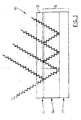
- a thin film, optically variable security device for incorporation into a document of value such as for example, a banknote, security card or other sheet-like substrate is shown and is generally identified by reference numeral 10.
- the security device 10 in the preferred embodiment is in the form of a thread that is designed to be woven into the document of value.
- security device 10 includes a carrier 12 and a multilayer coating 14 on the carrier.
- Carrier 12 in the preferred embodiment is formed of polyethylene teraphathalate (PET) commonly referred to as polyester.
- PET polyethylene teraphathalate
- Multilayer coating 14 is in the form of a metal-dielectric stack including an absorber layer 16 disposed on the carrier 12, a dielectric layer 18 disposed on the absorber layer 16 and a reflective layer 20 disposed on the dielectric layer 18.
- the absorber layer 16 is a semi-transparent Ni/Cr/Fe alloy commonly referred to as Inconel®.
- the dielectric layer 18 is formed of silicon dioxide (SiO 2 ) and the reflective layer 20 is formed of aluminum.
- the thickness of the absorber, dielectric and reflective layers 16 to 20 respectively are chosen so that the optically variable security device 10 exhibits the desired color shift with a change in the angle of incident light.
- a security device having an Inconel® absorber layer 16 with a thickness of 10nm, an SiO 2 dielectric layer 18 with a thickness of 350nm and an aluminum reflective layer 20 with an optical density of between about 2.0 to 2.5 and a reflectance greater than 90% at 500nm exhibits a very distinct magenta to green color shift with a change in view angle.
- suitable materials for the semi-transparent absorber layer 16 include chromium, nickel, aluminum, silver, copper, palladium, platinum, titanium, vanadium, cobalt, iron, tin, tungsten, molybdenum, rhodium, niobium, carbon, graphite, silicon, germanium and compounds, mixtures or alloys thereof.
- dielectric layer 18 suitable materials for the dielectric layer 18 include zinc sulfide, zinc oxide, zirconium oxide, zirconium dioxide, titanium dioxide, diamond-like carbon, indium cxide, indium-tin-oxide, tantalum pentoxide, cerium oxide, yttrium oxide, europium oxide, iron oxides, hafnium nitride, hafnium carbide, hafnium oxide, lanthanum oxide, magnesium oxide, magnesium fluoride, neodymium oxide, praseodymium oxide, samarium oxide, antimony trioxide, silicon monoxide, selenium trioxide, tin oxide, tungsten trioxide and combinations thereof as well as organic polymer acrylates.
- Suitable materials for the reflective layer 20 include chromium, nickel, silver, copper, gold, palladium, platinum, titanium, vanadium, cobalt, iron, tin, tungsten, molybdenum, rhodium, mioubium, carbon, graphite, silicon, germanium and compounds, mixtures or alloys thereof.
- the security device 10 once manufactured is typically sent to a third party, who tailors the security device 10 prior to incorporating the security device into the document of value.
- Figures 2a to 2c show the steps performed during tailoring of the security device 10.
- the reflective layer 20 is demetallized to include images, patterns and/or text. Tailoring the security device downstream of the security device manufacturing process is of course possible due to the fact that the reflective layer 20 of the multilayer coating 14 is exposed. In this manner, highly sensitive information including the identity of the end supplier of the document of value can be kept secret from the manufacturer of the security device 10
- the security device material can be fabricated and stockpiled ahead of time and demetallized just prior to delivery to reduce the typical long lead times associated with the production of such sophisticated technology.
- a PET cover layer 30 is bonded to the reflective layer 20.
- the multilayer coating 14 is protected against wear and chemical attack.
- the cover layer 30 and carrier 12 also help to improve handling.
- the security device 10 including the cover layer 30 is then coated with suitable adhesives and is incorporated into the document of value to secure it. Windows are provided in the document of value to expose the security device 10 so that its optically variable effect can be seen when looking at the secure document of value from different angles.
- FIG 3 shows various examples of a tailored security device 10.
- the reflective layer 20 in this case is tailored to include images, patterns and text including national symbols. Those of skill in the art will appreciate that any subset of images, patterns and text may be used to tailor the security device 10.
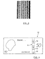
- Figure 4 shows a tailored security device 10 woven into a document of value in the form of a banknote 50.
- the reflective layer of the security device 10 is tailored to include text only.
- Windows 52 provided in the banknote 50 expose the security device at discrete locations.
- the security device With the security device incorporated into the document of valve, the security device provides the document of value with a variety of security attributes. For example, the security device exhibits a sharp color shift without the typical rainbox effect observed in other prior art optically variable devices and is resistant to physical and chemical attack. The color shift cannot be copied using modem reprographic methods. The color shift is easy to verify and to explain to the public making the security device simple for use by the public and document handlers.
- the security device can be used as a first level security feature and/or as a machine readable security feature.
- the carrier 12 can be embossed with an optical interference pattern or alternatively coated with a lacquer that is embossed with an optical interference pattern.
- the optical interference pattern may be selected from the group consisting of diffraction gratings, refraction patterns, holographic image patterns or combinations thereof.
- the optical interference pattern includes microstructures having dimensions in the range of from about 0.1 to 10 microns.
- the reflective layer 20 is described as being tailored through a demetallization process, those of skill in the art will appreciate that other techniques may be used to tailor the reflective layer. For example, images, patterns and/or text may be printed onto the reflective layer by various methods.
Landscapes
- Business, Economics & Management (AREA)
- Accounting & Taxation (AREA)
- Finance (AREA)
- Credit Cards Or The Like (AREA)
- Laminated Bodies (AREA)
- Disintegrating Or Milling (AREA)
- Diaphragms For Electromechanical Transducers (AREA)
- Inspection Of Paper Currency And Valuable Securities (AREA)
Applications Claiming Priority (2)
| Application Number | Priority Date | Filing Date | Title |
|---|---|---|---|
| US636786 | 1991-01-02 | ||
| US10/636,786 US7161738B2 (en) | 2003-08-07 | 2003-08-07 | Secure document of value and method of manufacturing same |
Publications (3)
| Publication Number | Publication Date |
|---|---|
| EP1504923A2 true EP1504923A2 (fr) | 2005-02-09 |
| EP1504923A3 EP1504923A3 (fr) | 2006-12-13 |
| EP1504923B1 EP1504923B1 (fr) | 2008-06-04 |
Family
ID=33552964
Family Applications (1)
| Application Number | Title | Priority Date | Filing Date |
|---|---|---|---|
| EP04254688A Expired - Lifetime EP1504923B1 (fr) | 2003-08-07 | 2004-08-05 | Document de valeur et la méthode de sa production |
Country Status (5)
| Country | Link |
|---|---|
| US (1) | US7161738B2 (fr) |
| EP (1) | EP1504923B1 (fr) |
| AT (1) | ATE397533T1 (fr) |
| CA (1) | CA2476228C (fr) |
| DE (1) | DE602004014219D1 (fr) |
Cited By (12)
| Publication number | Priority date | Publication date | Assignee | Title |
|---|---|---|---|---|
| US20120091702A1 (en) * | 2009-06-26 | 2012-04-19 | Merck Patent Gesellschaft Mit Beschrankter Haftung | Magnetic pigments comprising a flaky substrate and layer of maghemite |
| CN103350579A (zh) * | 2013-07-23 | 2013-10-16 | 长春市东方票证印务有限责任公司 | 一种防伪印刷方法 |
| WO2017080641A1 (fr) * | 2015-11-10 | 2017-05-18 | Giesecke & Devrient Gmbh | Élément de sécurité, procédé de fabrication de l'élément de sécurité, et support de données équipé de cet élément de sécurité |
| WO2017092865A1 (fr) * | 2015-12-01 | 2017-06-08 | Giesecke & Devrient Gmbh | Élément de sécurité et support de données équipé d'un tel élément de sécurité |
| WO2018210597A1 (fr) | 2017-05-15 | 2018-11-22 | Basf Se | Procédé pour la préparation de couches de nanoparticules métalliques et leur utilisation pour des éléments décoratifs ou de sécurité |
| WO2019016136A1 (fr) | 2017-07-20 | 2019-01-24 | Basf Se | Nanoparticules de dioxyde de titane fonctionnalisées en surface par phosphonate |
| WO2019020682A1 (fr) | 2017-07-28 | 2019-01-31 | Basf Se | Procédé de préparation de couches de nanoparticules métalliques et leur utilisation pour des éléments décoratifs ou de sécurité |
| EP3288770B1 (fr) | 2015-04-28 | 2019-06-26 | Giesecke+Devrient Currency Technology GmbH | Élément de sécurité à structure multicouche |
| WO2021052907A1 (fr) | 2019-09-17 | 2021-03-25 | Basf Se | Nanoparticules d'oxyde métallique |
| WO2022038161A1 (fr) | 2020-08-21 | 2022-02-24 | Basf Se | Revêtements durcissables aux uv ayant un indice de réfraction élevé |
| EP4234641A1 (fr) | 2022-02-25 | 2023-08-30 | Basf Se | Compositions comprenant des nanoparticules de dioxyde de titane modifiées et leurs utilisations |
| WO2024012962A1 (fr) | 2022-07-11 | 2024-01-18 | Basf Se | Revêtements durcissables aux uv ayant un indice de réfraction élevé |
Families Citing this family (10)
| Publication number | Priority date | Publication date | Assignee | Title |
|---|---|---|---|---|
| ITMI20051944A1 (it) * | 2005-10-14 | 2007-04-15 | Fabriano Securities Srl | Elemento di sicurezza per banconote o documenti rappresentanti un valore |
| GB0615919D0 (en) * | 2006-08-10 | 2006-09-20 | Rue De Int Ltd | Photonic crystal security device |
| GB0615921D0 (en) | 2006-08-10 | 2006-09-20 | Rue De Int Ltd | Photonic crystal security device |
| GB0720550D0 (en) | 2007-10-19 | 2007-11-28 | Rue De Int Ltd | Photonic crystal security device multiple optical effects |
| GB0906366D0 (en) | 2009-04-14 | 2009-05-20 | Rue De Int Ltd | Security device |
| GB0919112D0 (en) | 2009-10-30 | 2009-12-16 | Rue De Int Ltd | Security device |
| DE102009058243A1 (de) * | 2009-12-14 | 2011-06-16 | Giesecke & Devrient Gmbh | Dünnschichtelement mit Mehrschichtstruktur |
| GB2493369B (en) | 2011-08-02 | 2013-09-25 | Rue De Int Ltd | Improvements in security devices |
| JP6319985B2 (ja) * | 2013-10-11 | 2018-05-09 | インターナショナル・ビジネス・マシーンズ・コーポレーションInternational Business Machines Corporation | 光モジュール及び光モジュール製造方法。 |
| CN114551758A (zh) * | 2022-02-14 | 2022-05-27 | 深圳市华星光电半导体显示技术有限公司 | Oled显示面板及显示装置 |
Citations (2)
| Publication number | Priority date | Publication date | Assignee | Title |
|---|---|---|---|---|
| US3858977A (en) | 1972-01-18 | 1975-01-07 | Canadian Patents Dev | Optical interference authenticating means |
| US4186943A (en) | 1976-09-24 | 1980-02-05 | The Governor And Company Of The Bank Of England | Security devices |
Family Cites Families (6)
| Publication number | Priority date | Publication date | Assignee | Title |
|---|---|---|---|---|
| US4869778A (en) * | 1987-07-20 | 1989-09-26 | Gardoc, Inc. | Method of forming a patterned aluminum layer and article |
| GB8912750D0 (en) * | 1989-06-02 | 1989-07-19 | Portals Ltd | Security paper |
| DE4344553A1 (de) * | 1993-12-24 | 1995-06-29 | Giesecke & Devrient Gmbh | Sicherheitspapier mit einem faden- oder bandförmigen Sicherheitselement sowie Verfahren zur Herstellung desselben |
| DE19611383A1 (de) * | 1996-03-22 | 1997-09-25 | Giesecke & Devrient Gmbh | Datenträger mit optisch variablem Element |
| AU1194901A (en) * | 2000-01-21 | 2001-07-31 | Flex Products Inc | Optically variable security devices |
| DE10202035B4 (de) * | 2002-01-18 | 2018-10-18 | Giesecke+Devrient Currency Technology Gmbh | Sicherheitselement mit Farbkippeffekt und magnetischen Eigenschaften, Gegenstand mit einem solchen Sicherheitselement sowie Verfahren zur Herstellung des Sicherheitselements und des Gegenstands. |
-
2003
- 2003-08-07 US US10/636,786 patent/US7161738B2/en not_active Expired - Lifetime
-
2004
- 2004-08-03 CA CA2476228A patent/CA2476228C/fr not_active Expired - Lifetime
- 2004-08-05 EP EP04254688A patent/EP1504923B1/fr not_active Expired - Lifetime
- 2004-08-05 AT AT04254688T patent/ATE397533T1/de active
- 2004-08-05 DE DE602004014219T patent/DE602004014219D1/de not_active Expired - Lifetime
Patent Citations (2)
| Publication number | Priority date | Publication date | Assignee | Title |
|---|---|---|---|---|
| US3858977A (en) | 1972-01-18 | 1975-01-07 | Canadian Patents Dev | Optical interference authenticating means |
| US4186943A (en) | 1976-09-24 | 1980-02-05 | The Governor And Company Of The Bank Of England | Security devices |
Cited By (18)
| Publication number | Priority date | Publication date | Assignee | Title |
|---|---|---|---|---|
| KR101737652B1 (ko) * | 2009-06-26 | 2017-05-18 | 메르크 파텐트 게엠베하 | 박편상 기재 및 마그헤마이트 층을 포함하는 자성 안료 |
| US10174203B2 (en) * | 2009-06-26 | 2019-01-08 | Merck Patent Gmbh | Magnetic pigments comprising a flaky substrate and layer of maghemite |
| US20120091702A1 (en) * | 2009-06-26 | 2012-04-19 | Merck Patent Gesellschaft Mit Beschrankter Haftung | Magnetic pigments comprising a flaky substrate and layer of maghemite |
| CN103350579A (zh) * | 2013-07-23 | 2013-10-16 | 长春市东方票证印务有限责任公司 | 一种防伪印刷方法 |
| EP3288770B1 (fr) | 2015-04-28 | 2019-06-26 | Giesecke+Devrient Currency Technology GmbH | Élément de sécurité à structure multicouche |
| EP3288770B2 (fr) † | 2015-04-28 | 2024-08-21 | Giesecke+Devrient Currency Technology GmbH | Élément de sécurité à structure multicouche |
| WO2017080641A1 (fr) * | 2015-11-10 | 2017-05-18 | Giesecke & Devrient Gmbh | Élément de sécurité, procédé de fabrication de l'élément de sécurité, et support de données équipé de cet élément de sécurité |
| AU2016352335B2 (en) * | 2015-11-10 | 2019-09-19 | Giesecke+Devrient Currency Technology Gmbh | Security element, method for producing same, and data carrier equipped with the security element |
| WO2017092865A1 (fr) * | 2015-12-01 | 2017-06-08 | Giesecke & Devrient Gmbh | Élément de sécurité et support de données équipé d'un tel élément de sécurité |
| WO2018210597A1 (fr) | 2017-05-15 | 2018-11-22 | Basf Se | Procédé pour la préparation de couches de nanoparticules métalliques et leur utilisation pour des éléments décoratifs ou de sécurité |
| US11274219B2 (en) | 2017-07-20 | 2022-03-15 | Basf Se | Surface functionalized titanium dioxide nanoparticles |
| WO2019016136A1 (fr) | 2017-07-20 | 2019-01-24 | Basf Se | Nanoparticules de dioxyde de titane fonctionnalisées en surface par phosphonate |
| WO2019020682A1 (fr) | 2017-07-28 | 2019-01-31 | Basf Se | Procédé de préparation de couches de nanoparticules métalliques et leur utilisation pour des éléments décoratifs ou de sécurité |
| US11643561B2 (en) | 2017-07-28 | 2023-05-09 | Basf Se | Process for the preparation of metallic nano-particle layers and their use for decorative or security elements |
| WO2021052907A1 (fr) | 2019-09-17 | 2021-03-25 | Basf Se | Nanoparticules d'oxyde métallique |
| WO2022038161A1 (fr) | 2020-08-21 | 2022-02-24 | Basf Se | Revêtements durcissables aux uv ayant un indice de réfraction élevé |
| EP4234641A1 (fr) | 2022-02-25 | 2023-08-30 | Basf Se | Compositions comprenant des nanoparticules de dioxyde de titane modifiées et leurs utilisations |
| WO2024012962A1 (fr) | 2022-07-11 | 2024-01-18 | Basf Se | Revêtements durcissables aux uv ayant un indice de réfraction élevé |
Also Published As
| Publication number | Publication date |
|---|---|
| DE602004014219D1 (de) | 2008-07-17 |
| EP1504923A3 (fr) | 2006-12-13 |
| EP1504923B1 (fr) | 2008-06-04 |
| ATE397533T1 (de) | 2008-06-15 |
| CA2476228A1 (fr) | 2005-02-07 |
| US20050029800A1 (en) | 2005-02-10 |
| US7161738B2 (en) | 2007-01-09 |
| CA2476228C (fr) | 2010-09-21 |
Similar Documents
| Publication | Publication Date | Title |
|---|---|---|
| US7161738B2 (en) | Secure document of value and method of manufacturing same | |
| US8603615B2 (en) | Security element | |
| CN102089123B (zh) | 安全元件 | |
| EP3294568B1 (fr) | Dispositif de sécurité | |
| US8534710B2 (en) | Security element and method for manufacturing the same | |
| US6686027B1 (en) | Security substrate for documents of value | |
| CN100567022C (zh) | 防伪元件及带有该防伪元件的防伪文件 | |
| JP5448290B2 (ja) | 不可視の防犯用途の不透明フレークの周囲への枠または縁の設置 | |
| AU2010335962B2 (en) | Security devices, their production and use | |
| US11840112B2 (en) | Optical structures providing dichroic effects | |
| CN107531080A (zh) | 带有两个相互邻接的安全标记的安全元件 | |
| US7699351B2 (en) | Security document with a volume hologram forming a partial motif | |
| CN111093967A (zh) | 提供双色效应的光学结构 | |
| JP2016530118A (ja) | 回折光学要素を有するセキュリティ構造 | |
| US20180093519A1 (en) | Liquid crystal color-shifting security device | |
| CN101528473B (zh) | 具有液晶层的安全元件及其制造方法和用途、以及数据载体 | |
| CN108603344A (zh) | 安全元件和文件 | |
| CN112912254B (zh) | 光学显示体、页对、印刷制品、护照、卡、纸币、标签、标牌及票据 | |
| EP4182173B1 (fr) | Film de sécurité à double décalage de couleurs | |
| JPH0858224A (ja) | 情報担持体 | |
| KR101785467B1 (ko) | 색 변환 보안요소, 이의 제조방법 및 색 변환 보안요소를 포함하는 보안제품 | |
| RU2792958C1 (ru) | Защитный элемент со слоем с оптическим эффектом | |
| WO2019012550A1 (fr) | Film pour applications de sécurité | |
| CA2935159C (fr) | Dispositif de securite | |
| KR20210073138A (ko) | 보안 필름 및 이를 포함하는 보안제품 |
Legal Events
| Date | Code | Title | Description |
|---|---|---|---|
| PUAI | Public reference made under article 153(3) epc to a published international application that has entered the european phase |
Free format text: ORIGINAL CODE: 0009012 |
|
| AK | Designated contracting states |
Kind code of ref document: A2 Designated state(s): AT BE BG CH CY CZ DE DK EE ES FI FR GB GR HU IE IT LI LU MC NL PL PT RO SE SI SK TR |
|
| AX | Request for extension of the european patent |
Extension state: AL HR LT LV MK |
|
| 17P | Request for examination filed |
Effective date: 20060815 |
|
| PUAL | Search report despatched |
Free format text: ORIGINAL CODE: 0009013 |
|
| AK | Designated contracting states |
Kind code of ref document: A3 Designated state(s): AT BE BG CH CY CZ DE DK EE ES FI FR GB GR HU IE IT LI LU MC NL PL PT RO SE SI SK TR |
|
| AX | Request for extension of the european patent |
Extension state: AL HR LT LV MK |
|
| 17Q | First examination report despatched |
Effective date: 20070425 |
|
| AKX | Designation fees paid |
Designated state(s): AT BE BG CH CY CZ DE DK EE ES FI FR GB GR HU IE IT LI LU MC NL PL PT RO SE SI SK TR |
|
| RAP1 | Party data changed (applicant data changed or rights of an application transferred) |
Owner name: GIESECKE & DEVRIENT GMBH |
|
| GRAP | Despatch of communication of intention to grant a patent |
Free format text: ORIGINAL CODE: EPIDOSNIGR1 |
|
| GRAS | Grant fee paid |
Free format text: ORIGINAL CODE: EPIDOSNIGR3 |
|
| GRAA | (expected) grant |
Free format text: ORIGINAL CODE: 0009210 |
|
| AK | Designated contracting states |
Kind code of ref document: B1 Designated state(s): AT BE BG CH CY CZ DE DK EE ES FI FR GB GR HU IE IT LI LU MC NL PL PT RO SE SI SK TR |
|
| REG | Reference to a national code |
Ref country code: GB Ref legal event code: FG4D |
|
| REG | Reference to a national code |
Ref country code: CH Ref legal event code: EP |
|
| REF | Corresponds to: |
Ref document number: 602004014219 Country of ref document: DE Date of ref document: 20080717 Kind code of ref document: P |
|
| REG | Reference to a national code |
Ref country code: CH Ref legal event code: NV Representative=s name: PATENTANWAELTE SCHAAD, BALASS, MENZL & PARTNER AG |
|
| REG | Reference to a national code |
Ref country code: SE Ref legal event code: TRGR |
|
| REG | Reference to a national code |
Ref country code: IE Ref legal event code: FG4D |
|
| PG25 | Lapsed in a contracting state [announced via postgrant information from national office to epo] |
Ref country code: FI Free format text: LAPSE BECAUSE OF FAILURE TO SUBMIT A TRANSLATION OF THE DESCRIPTION OR TO PAY THE FEE WITHIN THE PRESCRIBED TIME-LIMIT Effective date: 20080604 Ref country code: SI Free format text: LAPSE BECAUSE OF FAILURE TO SUBMIT A TRANSLATION OF THE DESCRIPTION OR TO PAY THE FEE WITHIN THE PRESCRIBED TIME-LIMIT Effective date: 20080604 Ref country code: ES Free format text: LAPSE BECAUSE OF FAILURE TO SUBMIT A TRANSLATION OF THE DESCRIPTION OR TO PAY THE FEE WITHIN THE PRESCRIBED TIME-LIMIT Effective date: 20080915 |
|
| PG25 | Lapsed in a contracting state [announced via postgrant information from national office to epo] |
Ref country code: PL Free format text: LAPSE BECAUSE OF FAILURE TO SUBMIT A TRANSLATION OF THE DESCRIPTION OR TO PAY THE FEE WITHIN THE PRESCRIBED TIME-LIMIT Effective date: 20080604 Ref country code: NL Free format text: LAPSE BECAUSE OF FAILURE TO SUBMIT A TRANSLATION OF THE DESCRIPTION OR TO PAY THE FEE WITHIN THE PRESCRIBED TIME-LIMIT Effective date: 20080604 |
|
| NLV1 | Nl: lapsed or annulled due to failure to fulfill the requirements of art. 29p and 29m of the patents act | ||
| PG25 | Lapsed in a contracting state [announced via postgrant information from national office to epo] |
Ref country code: CZ Free format text: LAPSE BECAUSE OF FAILURE TO SUBMIT A TRANSLATION OF THE DESCRIPTION OR TO PAY THE FEE WITHIN THE PRESCRIBED TIME-LIMIT Effective date: 20080604 Ref country code: PT Free format text: LAPSE BECAUSE OF FAILURE TO SUBMIT A TRANSLATION OF THE DESCRIPTION OR TO PAY THE FEE WITHIN THE PRESCRIBED TIME-LIMIT Effective date: 20081104 |
|
| PG25 | Lapsed in a contracting state [announced via postgrant information from national office to epo] |
Ref country code: RO Free format text: LAPSE BECAUSE OF FAILURE TO SUBMIT A TRANSLATION OF THE DESCRIPTION OR TO PAY THE FEE WITHIN THE PRESCRIBED TIME-LIMIT Effective date: 20080604 Ref country code: SK Free format text: LAPSE BECAUSE OF FAILURE TO SUBMIT A TRANSLATION OF THE DESCRIPTION OR TO PAY THE FEE WITHIN THE PRESCRIBED TIME-LIMIT Effective date: 20080604 Ref country code: BE Free format text: LAPSE BECAUSE OF FAILURE TO SUBMIT A TRANSLATION OF THE DESCRIPTION OR TO PAY THE FEE WITHIN THE PRESCRIBED TIME-LIMIT Effective date: 20080604 |
|
| PG25 | Lapsed in a contracting state [announced via postgrant information from national office to epo] |
Ref country code: MC Free format text: LAPSE BECAUSE OF NON-PAYMENT OF DUE FEES Effective date: 20080831 |
|
| PLBE | No opposition filed within time limit |
Free format text: ORIGINAL CODE: 0009261 |
|
| STAA | Information on the status of an ep patent application or granted ep patent |
Free format text: STATUS: NO OPPOSITION FILED WITHIN TIME LIMIT |
|
| PG25 | Lapsed in a contracting state [announced via postgrant information from national office to epo] |
Ref country code: DK Free format text: LAPSE BECAUSE OF FAILURE TO SUBMIT A TRANSLATION OF THE DESCRIPTION OR TO PAY THE FEE WITHIN THE PRESCRIBED TIME-LIMIT Effective date: 20080604 Ref country code: EE Free format text: LAPSE BECAUSE OF FAILURE TO SUBMIT A TRANSLATION OF THE DESCRIPTION OR TO PAY THE FEE WITHIN THE PRESCRIBED TIME-LIMIT Effective date: 20080604 Ref country code: BG Free format text: LAPSE BECAUSE OF FAILURE TO SUBMIT A TRANSLATION OF THE DESCRIPTION OR TO PAY THE FEE WITHIN THE PRESCRIBED TIME-LIMIT Effective date: 20080904 |
|
| 26N | No opposition filed |
Effective date: 20090305 |
|
| PG25 | Lapsed in a contracting state [announced via postgrant information from national office to epo] |
Ref country code: IE Free format text: LAPSE BECAUSE OF NON-PAYMENT OF DUE FEES Effective date: 20080805 |
|
| PG25 | Lapsed in a contracting state [announced via postgrant information from national office to epo] |
Ref country code: IT Free format text: LAPSE BECAUSE OF NON-PAYMENT OF DUE FEES Effective date: 20080805 |
|
| PG25 | Lapsed in a contracting state [announced via postgrant information from national office to epo] |
Ref country code: LU Free format text: LAPSE BECAUSE OF NON-PAYMENT OF DUE FEES Effective date: 20080805 Ref country code: CY Free format text: LAPSE BECAUSE OF FAILURE TO SUBMIT A TRANSLATION OF THE DESCRIPTION OR TO PAY THE FEE WITHIN THE PRESCRIBED TIME-LIMIT Effective date: 20080604 Ref country code: HU Free format text: LAPSE BECAUSE OF FAILURE TO SUBMIT A TRANSLATION OF THE DESCRIPTION OR TO PAY THE FEE WITHIN THE PRESCRIBED TIME-LIMIT Effective date: 20081205 |
|
| PG25 | Lapsed in a contracting state [announced via postgrant information from national office to epo] |
Ref country code: TR Free format text: LAPSE BECAUSE OF FAILURE TO SUBMIT A TRANSLATION OF THE DESCRIPTION OR TO PAY THE FEE WITHIN THE PRESCRIBED TIME-LIMIT Effective date: 20080604 |
|
| PG25 | Lapsed in a contracting state [announced via postgrant information from national office to epo] |
Ref country code: GR Free format text: LAPSE BECAUSE OF FAILURE TO SUBMIT A TRANSLATION OF THE DESCRIPTION OR TO PAY THE FEE WITHIN THE PRESCRIBED TIME-LIMIT Effective date: 20080905 |
|
| PGRI | Patent reinstated in contracting state [announced from national office to epo] |
Ref country code: IT Effective date: 20110616 |
|
| REG | Reference to a national code |
Ref country code: DE Ref legal event code: R082 Ref document number: 602004014219 Country of ref document: DE |
|
| REG | Reference to a national code |
Ref country code: FR Ref legal event code: PLFP Year of fee payment: 13 |
|
| REG | Reference to a national code |
Ref country code: FR Ref legal event code: PLFP Year of fee payment: 14 |
|
| REG | Reference to a national code |
Ref country code: DE Ref legal event code: R081 Ref document number: 602004014219 Country of ref document: DE Owner name: GIESECKE+DEVRIENT CURRENCY TECHNOLOGY GMBH, DE Free format text: FORMER OWNER: GIESECKE DEVRIENT GMBH, 81677 MUENCHEN, DE Ref country code: DE Ref legal event code: R081 Ref document number: 602004014219 Country of ref document: DE Owner name: GIESECKE+DEVRIENT CURRENCY TECHNOLOGY GMBH, DE Free format text: FORMER OWNER: GIESECKE & DEVRIENT GMBH, 81677 MUENCHEN, DE |
|
| REG | Reference to a national code |
Ref country code: CH Ref legal event code: PUE Owner name: GIESECKE+DEVRIENT CURRENCY TECHNOLOGY GMBH, DE Free format text: FORMER OWNER: GIESECKE AND DEVRIENT GMBH, DE |
|
| REG | Reference to a national code |
Ref country code: GB Ref legal event code: 732E Free format text: REGISTERED BETWEEN 20180118 AND 20180124 |
|
| REG | Reference to a national code |
Ref country code: AT Ref legal event code: PC Ref document number: 397533 Country of ref document: AT Kind code of ref document: T Owner name: GIESECKE+DEVRIENT CURRENCY TECHNOLOGY GMBH, DE Effective date: 20180425 |
|
| REG | Reference to a national code |
Ref country code: FR Ref legal event code: TP Owner name: GIESECKE+DEVRIENT CURRENCY TECHNOLOGY GMBH, DE Effective date: 20180530 |
|
| REG | Reference to a national code |
Ref country code: FR Ref legal event code: PLFP Year of fee payment: 15 |
|
| PGFP | Annual fee paid to national office [announced via postgrant information from national office to epo] |
Ref country code: SE Payment date: 20190826 Year of fee payment: 16 |
|
| PGFP | Annual fee paid to national office [announced via postgrant information from national office to epo] |
Ref country code: CH Payment date: 20190826 Year of fee payment: 16 |
|
| REG | Reference to a national code |
Ref country code: SE Ref legal event code: EUG |
|
| REG | Reference to a national code |
Ref country code: CH Ref legal event code: PL |
|
| PG25 | Lapsed in a contracting state [announced via postgrant information from national office to epo] |
Ref country code: CH Free format text: LAPSE BECAUSE OF NON-PAYMENT OF DUE FEES Effective date: 20200831 Ref country code: LI Free format text: LAPSE BECAUSE OF NON-PAYMENT OF DUE FEES Effective date: 20200831 |
|
| PG25 | Lapsed in a contracting state [announced via postgrant information from national office to epo] |
Ref country code: SE Free format text: LAPSE BECAUSE OF NON-PAYMENT OF DUE FEES Effective date: 20200806 |
|
| P01 | Opt-out of the competence of the unified patent court (upc) registered |
Effective date: 20230520 |
|
| PGFP | Annual fee paid to national office [announced via postgrant information from national office to epo] |
Ref country code: IT Payment date: 20230831 Year of fee payment: 20 Ref country code: GB Payment date: 20230824 Year of fee payment: 20 Ref country code: AT Payment date: 20230818 Year of fee payment: 20 |
|
| PGFP | Annual fee paid to national office [announced via postgrant information from national office to epo] |
Ref country code: FR Payment date: 20230822 Year of fee payment: 20 Ref country code: DE Payment date: 20230831 Year of fee payment: 20 |
|
| REG | Reference to a national code |
Ref country code: DE Ref legal event code: R071 Ref document number: 602004014219 Country of ref document: DE |
|
| REG | Reference to a national code |
Ref country code: GB Ref legal event code: PE20 Expiry date: 20240804 |
|
| REG | Reference to a national code |
Ref country code: AT Ref legal event code: MK07 Ref document number: 397533 Country of ref document: AT Kind code of ref document: T Effective date: 20240805 |
|
| PG25 | Lapsed in a contracting state [announced via postgrant information from national office to epo] |
Ref country code: GB Free format text: LAPSE BECAUSE OF EXPIRATION OF PROTECTION Effective date: 20240804 |
|
| PG25 | Lapsed in a contracting state [announced via postgrant information from national office to epo] |
Ref country code: GB Free format text: LAPSE BECAUSE OF EXPIRATION OF PROTECTION Effective date: 20240804 |