EP1505486A2 - Eingabegerät - Google Patents
Eingabegerät Download PDFInfo
- Publication number
- EP1505486A2 EP1505486A2 EP04254385A EP04254385A EP1505486A2 EP 1505486 A2 EP1505486 A2 EP 1505486A2 EP 04254385 A EP04254385 A EP 04254385A EP 04254385 A EP04254385 A EP 04254385A EP 1505486 A2 EP1505486 A2 EP 1505486A2
- Authority
- EP
- European Patent Office
- Prior art keywords
- resistance
- low
- resistor
- input device
- series
- Prior art date
- Legal status (The legal status is an assumption and is not a legal conclusion. Google has not performed a legal analysis and makes no representation as to the accuracy of the status listed.)
- Withdrawn
Links
Images



Classifications
-
- H—ELECTRICITY
- H01—ELECTRIC ELEMENTS
- H01H—ELECTRIC SWITCHES; RELAYS; SELECTORS; EMERGENCY PROTECTIVE DEVICES
- H01H25/00—Switches with compound movement of handle or other operating part
- H01H25/04—Operating part movable angularly in more than one plane, e.g. joystick
- H01H25/041—Operating part movable angularly in more than one plane, e.g. joystick having a generally flat operating member depressible at different locations to operate different controls
-
- G—PHYSICS
- G06—COMPUTING OR CALCULATING; COUNTING
- G06F—ELECTRIC DIGITAL DATA PROCESSING
- G06F1/00—Details not covered by groups G06F3/00 - G06F13/00 and G06F21/00
- G06F1/26—Power supply means, e.g. regulation thereof
- G06F1/32—Means for saving power
- G06F1/3203—Power management, i.e. event-based initiation of a power-saving mode
-
- G—PHYSICS
- G06—COMPUTING OR CALCULATING; COUNTING
- G06F—ELECTRIC DIGITAL DATA PROCESSING
- G06F1/00—Details not covered by groups G06F3/00 - G06F13/00 and G06F21/00
- G06F1/26—Power supply means, e.g. regulation thereof
- G06F1/32—Means for saving power
- G06F1/3203—Power management, i.e. event-based initiation of a power-saving mode
- G06F1/3234—Power saving characterised by the action undertaken
- G06F1/325—Power saving in peripheral device
- G06F1/3259—Power saving in cursor control device, e.g. mouse, joystick, trackball
-
- G—PHYSICS
- G06—COMPUTING OR CALCULATING; COUNTING
- G06F—ELECTRIC DIGITAL DATA PROCESSING
- G06F3/00—Input arrangements for transferring data to be processed into a form capable of being handled by the computer; Output arrangements for transferring data from processing unit to output unit, e.g. interface arrangements
- G06F3/01—Input arrangements or combined input and output arrangements for interaction between user and computer
- G06F3/03—Arrangements for converting the position or the displacement of a member into a coded form
- G06F3/033—Pointing devices displaced or positioned by the user, e.g. mice, trackballs, pens or joysticks; Accessories therefor
- G06F3/0338—Pointing devices displaced or positioned by the user, e.g. mice, trackballs, pens or joysticks; Accessories therefor with detection of limited linear or angular displacement of an operating part of the device from a neutral position, e.g. isotonic or isometric joysticks
-
- H—ELECTRICITY
- H01—ELECTRIC ELEMENTS
- H01H—ELECTRIC SWITCHES; RELAYS; SELECTORS; EMERGENCY PROTECTIVE DEVICES
- H01H2215/00—Tactile feedback
- H01H2215/004—Collapsible dome or bubble
- H01H2215/006—Only mechanical function
-
- H—ELECTRICITY
- H01—ELECTRIC ELEMENTS
- H01H—ELECTRIC SWITCHES; RELAYS; SELECTORS; EMERGENCY PROTECTIVE DEVICES
- H01H2239/00—Miscellaneous
- H01H2239/078—Variable resistance by variable contact area or point
-
- H—ELECTRICITY
- H01—ELECTRIC ELEMENTS
- H01H—ELECTRIC SWITCHES; RELAYS; SELECTORS; EMERGENCY PROTECTIVE DEVICES
- H01H2300/00—Orthogonal indexing scheme relating to electric switches, relays, selectors or emergency protective devices covered by H01H
- H01H2300/022—Application wake up; switches or contacts specially provided for the wake up or standby shift of a circuit
-
- Y—GENERAL TAGGING OF NEW TECHNOLOGICAL DEVELOPMENTS; GENERAL TAGGING OF CROSS-SECTIONAL TECHNOLOGIES SPANNING OVER SEVERAL SECTIONS OF THE IPC; TECHNICAL SUBJECTS COVERED BY FORMER USPC CROSS-REFERENCE ART COLLECTIONS [XRACs] AND DIGESTS
- Y02—TECHNOLOGIES OR APPLICATIONS FOR MITIGATION OR ADAPTATION AGAINST CLIMATE CHANGE
- Y02D—CLIMATE CHANGE MITIGATION TECHNOLOGIES IN INFORMATION AND COMMUNICATION TECHNOLOGIES [ICT], I.E. INFORMATION AND COMMUNICATION TECHNOLOGIES AIMING AT THE REDUCTION OF THEIR OWN ENERGY USE
- Y02D10/00—Energy efficient computing, e.g. low power processors, power management or thermal management
-
- Y—GENERAL TAGGING OF NEW TECHNOLOGICAL DEVELOPMENTS; GENERAL TAGGING OF CROSS-SECTIONAL TECHNOLOGIES SPANNING OVER SEVERAL SECTIONS OF THE IPC; TECHNICAL SUBJECTS COVERED BY FORMER USPC CROSS-REFERENCE ART COLLECTIONS [XRACs] AND DIGESTS
- Y02—TECHNOLOGIES OR APPLICATIONS FOR MITIGATION OR ADAPTATION AGAINST CLIMATE CHANGE
- Y02D—CLIMATE CHANGE MITIGATION TECHNOLOGIES IN INFORMATION AND COMMUNICATION TECHNOLOGIES [ICT], I.E. INFORMATION AND COMMUNICATION TECHNOLOGIES AIMING AT THE REDUCTION OF THEIR OWN ENERGY USE
- Y02D30/00—Reducing energy consumption in communication networks
- Y02D30/50—Reducing energy consumption in communication networks in wire-line communication networks, e.g. low power modes or reduced link rate
Definitions
- the present invention relates to input devices whose output is changed based on a change in pressing stroke or in pressure when pressing an operating object, and in particular, to an input device in which power consumption in a no-operation state is reduced.
- Input devices for game machines and personal computers include those whose output is changed in analog form based on a change in pressing stroke or pressure.
- a so-called "click rubber member” such as a silicone rubber member, opposes an electrode provided on a base, and the click rubber member is supplied with pulse power.
- the click rubber member By operating a key top to allow the click rubber member to touch the electrode, electricity flows as an output.
- the click rubber member onto the electrode By pressing the click rubber member onto the electrode to elastically deform, the output is changed based on the amount of deformation.
- the present invention is intended to solve the above problems, and it is an object of the present invention to provide an input device in which no wasteful power consumption occurs when an operating object is not operated, and in which, as soon as the operating object is operated, the input device enters a detection mode.
- an input device which includes at least one resistance-element series formed by a plurality of resistance elements connected in series, low resistors respectively opposing the resistance elements, an operating object which brings one low resistor into contact with one resistance element and which changes the contact area therebetween, an output point provided at the midpoint between resistance elements of the resistance-element series, and a controller in which (a) when the resistance element and the low resistor are not in contact, the controller sets a sleep mode for setting one of the resistance-element series and each low resistor to have a high potential, and setting the other one to have a low potential, (b) in the sleep mode, the controller monitors the occurrence of a change in voltage or current on the low potential side, and, when a change is detected, the controller determines that the operating object has been operated, and (c) after the determination, the controller applies a voltage across ends of the resistance-element series, and sets a detection mode for obtaining, from the output point, an output based on a change in contact area
- the number of resistance-element series is more than one, and the resistance-element series are connected in parallel.
- Each of the resistance-element series may have two resistance elements.
- the number of resistance-element series is two and the two resistance-element series may be connected in parallel.
- the resistance elements may be disposed at intervals in two directions perpendicular to each other.
- the operating object may be used to move each of the low resistors which opposes each of the resistance elements.
- the ends of the resistance-element series may be set to have high potentials, and each low resistor may be set to have a low potential, and by detecting a change in potential or current in the low resistors, the controller determines whether or not the operating object has been operated.
- each low resistor may be set to have a high impedance.
- the ends of the resistance-element series may be set to have low potentials, each low resistor may be set to have a high potential, and, by detecting a change in potential or current in the low resistors, the controller may determine that the operating object has been operated.
- a voltage obtained from the output point may be stored as a reference value.
- the voltage obtained from the output point may be used to update the reference value at regular time intervals.
- the present invention by obtaining an output from the midpoint between resistance-element series formed by resistance elements connected in series, when the contact area between each resistance element and each low resistor with reference to the midpoint is changed, positive and negative analog outputs with the potential of the midpoint used as a reference can be obtained.
- resistance-element series of the above type in parallel, for example, positive and analog outputs in two different directions can be obtained.
- a detection mode in a sleep mode, the power consumption of the resistance elements can be reduced or nullified. Also, after it is detected that an object has been operated, a detection mode can immediately be set.
- the zero points of positive and analog outputs can accurately be set.
- Fig. 1 is a perspective view showing the entire structure of a four-direction input device according to a first embodiment of the present invention.
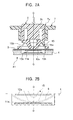
- Figs. 2A and 2B are sectional views taken on the line II-II shown in Fig. 1.
- Fig. 3 is a circuit diagram showing the four-direction input device.
- Fig. 4 is an equivalent circuit diagram illustrating a sleep mode.
- Fig. 5 is an equivalent circuit diagram illustrating a detection mode.
- Fig. 6 is an operation flowchart.
- the four-direction input device 1 shown in Fig. 1 has four detecting sections X1, X2, Y1, and Y2, and an operating object 2 for operating the detecting sections X1, X2, Y1, and Y2.
- the detecting sections X1, X2, Y1, and Y2 are disposed at regular intervals in two directions perpendicular to each other.
- the detecting sections X1, X2, Y1, and Y2 are provided on a base 4.
- the planar shape of the operating object 2 is a cross. Its arms extending in four directions have a first operating section 2a for operating the detecting section X1, a second operating section 2b for operating the detecting section X2, a third operating section 2c for operating the detecting section Y1, and a fourth operating section 2d for operating the detecting section Y2.
- a supporting projection 3 is formed in a form integrated with the bottom face. Accordingly, by using, as the fulcrum, the contact point between the supporting projection 3 and the base 4, the operating object 2 is capable of inclining movement in all the directions.
- Fig. 2A is a sectional view showing the structure of the detecting section X1 and the first operating section 2a.
- a resistance element 11a fixed to the base 4 is provided on the base 4, a flexible and insulating film 5 is disposed.
- a low resistor 12a is fixed to the film 5, and the low resistor 12a opposes the resistance element 11a, having space therebetween.
- the resistance element 11a is a carbon film or the like, and its pattern is rectangular. Electrode films 13a and 13b are connected across the resistance element 11a.
- the low resistor 12a has an electrical resistance lower than that of the resistance element 11a, and is a film of metal such as silver, gold, or copper.
- the resistance element 11a and the low resistor 12a may be formed of any materials if both have a difference in resistance.
- the low resistor 12a is formed in, for example, a circular pattern.
- an elastic pressing member 15 is provided on an upper face of the film 5.
- the elastic pressing member 15 is formed of rubber material.
- the elastic pressing member 15 is formed such that a compressively deformable pressing part 15a and a thin compressively-deformable rib 15b for preventing the pressing part 15a from inclining are formed in integrated form.
- the elastic pressing member 15 can be pressed by the first operating section 2a of the operating object 2.
- a case 7 is disposed above the base 4, with a distance provided therebetween.
- a cross opening 7a is formed.
- the operating object 2 is positioned inside the opening 7a, and the upper face of the operating object 2 protrudes upward from the case 7. Accordingly, the operating sections 2a, 2b, 2c, and 2d of the operating object 2 can be pressed.
- a locking mechanism for preventing the operating object 2 from coming out upward from the opening 7a is provided, it is not shown in Figs. 1, 2A, and 2B.
- the first operating section 2a presses the elastic pressing member 15.
- the film 5 is elastically deformed by the elastic pressing member 15, and the low resistor 12a touches the resistance element 11a.
- the pressing part 15a of the elastic pressing member 15 is compressively deformed and the film 5 further warps, so that the contact area between the resistance element 11a and the low resistor 12a increases.
- the contact area between the resistance element 11a and the low resistor 12a increases. This increase in contact area reduces the electrical resistance between the electrode films 13a and 13b. In other words, as the pressing stroke or pressure when pressing the first operating section 2a becomes enhanced, the electrical resistance between the electrodes films 13a and 13b changes in analog form.
- the structures of the detecting sections X2, Y1, and Y2 are each identical to that of the detecting section X1.
- a resistance element provided in the detecting section X2 is represented by 11b
- a low resistance element provided in the detecting section X is represented by 12b
- a resistance element and low resistance element provided in the detecting section Y1 are represented by 11c and 12c, respectively
- a resistance element and low resistance element provided in the detecting section Y2 are represented by 11d and 12d, respectively.
- the resistance element 11a in the detecting section X2 and the resistance element 11b in the detecting section X2 are connected in series to form a resistance-element series 14X
- the resistance element 11c in the detecting section Y1 and the resistance element 11d in the detecting section Y2 are connected in series to form a resistance-element series 14Y.
- the resistance-element series 14X and the resistance-element series 14Y are connected in parallel.
- a controller 30 that controls the four-direction input device 1 is an integrated circuit including a central processing unit (CPU), a storage unit, an analog-to-digital (A/D) converting unit for supplying the CPU with a digital signal obtained by converting an analog input signal, a switch unit (switching port), and an input unit (input port).
- CPU central processing unit
- A/D analog-to-digital
- the midpoint between the resistance element 11a and the resistance element 11b is an X-output point 15X.
- the midpoint between the resistance element 11c and the resistance element 11d is a Y-output point 15Y.
- a voltage obtained at the X-output point 15X is supplied to an X-input A/D converting unit 31.
- a voltage obtained at the Y-output point 15Y is supplied to a Y-input A/D converting unit 32.
- a parallel connection point 16a connected in parallel to one of the resistance-element series 14X and the resistance-element series 14Y is supplied with a power-supply voltage Vdd.
- a parallel connection point 16b connected in parallel to the other one of the resistance-element series 14X and the resistance-element series 14Y is connected to a switching unit 33 in the controller 30.
- the switching unit 33 is switched to have ground potential or the power-supply voltage Vdd.
- the low resistor 12a in the detecting section X1 is connected to an input unit 34a of the controller 30, and the low resistor 12b in the detecting section X2 is connected to an input unit 34b.
- the low resistor 12c is connected to an input unit 34c
- the low resistor 12d in the detecting section Y2 is connected to an input unit 34d.
- Each of the input units 34a, 34b, 34c, and 34d has an input-unit function of detecting the state of high potential or low potential.
- the input units 34a, 34b, 34c, and 34d can be set to have high impedances.
- the low resistor 12a in the detecting section X1 is connected to a switching unit 35a in the controller 30 by an external resistor Ra.
- the low resistor 12b is connected to a switching unit 35b by a resistor Rb.
- the low resistor 12c is connected to a switching unit 35c by a resistor Rc.
- the low resistor 12d is connected to a switching unit 35d by a resistor Rd.
- Each of the switching units 35a, 35b, 35c, and 35d is switched to have the ground potential or a high impedance.
- Fig. 4 illustrates a state in which the sleep mode is set by the controller 30.
- the switching unit 33 In the sleep mode, the switching unit 33 is set to have a power-supply voltage Vdd, and both the parallel connection points 16a and 16b are set to have the same power-supply voltage Vdd (high potential).
- the switching units 35a, 35b, 35c, and 35d are switched to have the ground potential. Ends of the resistors Ra, Rb, Rc, and Rd which are reverse to ends connected to the resistors 12a, 12b, 12c, and 12d are set to have the ground potential.
- the CPU in the controller 30 enters a mode that monitors the potentials of the input units 34a, 34b, 34c, and 34d.
- the resistance element 11a and the low resistor 12a are not in contact, and also in the detecting sections X2, Y1, and Y2, the resistance elements 11b, 11c, and 11d are not in contact with the low resistors 12b, 12c, and 12d, respectively.
- the input units 34a, 34b, 34c, and 34d still have low potentials. Therefore, the CPU recognizes that the operating object 2 is not operated.
- ends of the resistance-element series 14X and the resistance-element series 14Y are set to have the same power-supply voltage Vdd.
- Vdd power-supply voltage
- the parallel connection points 16a and 16b have a potential difference therebetween, the difference is small. Accordingly, by increasing the resistances of the resistance elements 11a, 11b, 11c, and 11d, almost no currents flow in these resistance elements.
- a detection mode is set in the controller 30.
- the switching unit 33 in the detection mode, is set to have the ground potential, and a potential difference (power-supply voltage Vdd) is given between the parallel connection points 16a and 16b. In other words, both ends of the resistance-element series 14X and 14Y are supplied with potential difference (power-supply voltage Vdd).
- the input units 34a, 34b, 34c, and 34d, and the switching units 35a, 35b, 35c, and 35d are set to have high impedances.
- the low resistor 12a touches the resistance element 11a to change the contact area, and the resistance in the detecting section X1 decreases, the voltage supplied to the X-input A/D converting unit 31 increases than the intermediate potential.
- This voltage is changed in analog form by changing a pressing stroke or the pressure obtained when pressing the first operating section 2a.
- the low resistor 12b touches the resistance element 11b to change the contact area, and the resistance in the detecting section X2 decreases, the voltage supplied to the X-input A/D converting unit 31 decreases than the intermediate potential.
- the voltage supplied to the X-input A/D converting unit 31 is changed in analog form in a positive direction when the first operating section 2a is pressed, and is changed in analog form in a negative direction when the second operating section 2b is pressed.
- the voltage supplied to the Y-input A/D converting unit 32 is changed in analog form in a positive direction when the third operating section 2c is pressed, and is changed in analog form in a negative direction when the fourth operating section 2d is pressed.
- analog X-direction inputting and analog Y-direction inputting can be performed.
- combining pressing operations of the operating sections 2a to 2d enables analog multi-directional input represented by ⁇ (X 2 +Y 2 ).
- the input points 34a, 34b, 34c, and 34d, and the switching units 35a, 35b, 35c, and 35d have high impedances.
- the low resistor and the resistance element are in contact in any detecting section, no currents flow into the input points 34a, 34b, 34c, and 34d, and the switching units 35a, 35b, 35c, and 35d.
- step ST1 By switching on the power of an apparatus using the four-direction input device 1 (step ST1), the sleep mode shown in Fig. 4 is set (step ST2), and the four-direction input device 1 enters an initializing operation (step ST3).
- This initializing operation is performed after recognizing that, in each of the detecting sections X1, X2, Y1, and Y2, the low resistor is not in contact with the resistance element, that is, any of the input units 34a, 34b, 34c, and 34d has a low potential (step ST4).
- the detection mode shown in Fig. 5 is set (step ST5), and the voltage of the X-output point 15X is captured by the X-input A/D converting unit 31. This voltage is stored as an X-direction-output center value (X-direction reference value) in the controller 30.
- the voltage of the Y-output point 15Y is captured by the Y-input A/D converting unit 32, and this voltage is stored as a Y-direction-output center value (Y-direction reference value) in the controller 30 (steps ST6 and ST7).
- the X-direction-output center value means the mid-value of divisors (e.g., "128", "256”, etc.) of a digital value which is converted by the X-input A/D converting unit 31.
- the voltage of the X-output point 15X is stored as the center value of the divisors in the storage unit, and the voltage of the Y-output point 15Y is stored as the center value of the divisors in the storage unit (step ST7).
- step ST8 the sleep mode shown in Fig. 4 is set.
- step ST9 in the sleep mode, any of the detecting sections X1, X2, Y1, and Y2 is monitored about whether the low resistor is in contact with the resistance element.
- the contact between the low resistor and the resistance element causes one of the input units 34a, 34b, 34c, and 34d to have a high potential
- the four-direction input device 1 enters the detection mode shown in Fig. 5 (step ST10).
- step ST10 When, in the detection mode in step ST10, an operation on the operating object 2 changes the potentials of the X-output point 15X and the Y-output point 15Y, the voltages are converted into digital form by the X-input A/D converting unit 31 and the Y-input A/D converting unit 32 (step ST11).
- the CPU in the controller 30 calculates a difference between the digital converted value of X-input and the center value in the Y-direction, and recognizes the difference as an X-direction analog coordinate input value.
- the CPU calculates a difference between the digital converted value of Y-input and the center value in the Y-direction, and recognizes the difference as an Y-direction analog coordinate input value (step ST12).
- step ST9 After the sleep mode is set in step ST8, it is determined in step ST9 that a state in which, in any of the detecting sections X1, X2, Y1, and Y2, the low resistor is not in contact with the resistance element has continued for a predetermined time (T1) (step ST13), the process returns to ST5, and the X-direction center value and the Y-direction center value are updated by the outputs of the X-output point 15X and the Y-output point 15Y.
- T1 predetermined time
- the sleep mode by setting the sleep mode when the operating object 2 is not operated, power consumption can be reduced. If the state in which the operating object 2 is not operated has continued for the T1 time, the sleep mode is changed into the initializing mode, and the X-direction center value and the Y-direction center value are updated. Therefore, even if the resistances of the resistance elements 11a, 11b, 11c, and 11d are not exactly equal, and these resistance vary due to a change in temperature, or the like, the center value of the divisors in digital of the X-direction input and the Y-direction input is constantly updated before changing into the detection operation, thus realizing accurate X-Y coordinate input.
- Fig. 7 is a circuit diagram showing a four-direction input device according to a second embodiment of the present invention.
- the second embodiment by using identical reference numerals to denote portions identical to those in the first embodiment, a detailed description of the portions is omitted.
- low resistors 12a, 12b, 12c, and 12d in detecting sections X1, X2, Y1, and Y2 are connected to a single input unit 34e in a controller 30A.
- a resistor R is provided and the low resistors 12a, 12b, 12c, and 12d are connected to a switching unit 37 by the resistor R.
- the switching unit 37 is switched to have a power-supply voltage Vdd or a high impedance.
- the switching unit 37 may be such that it is continuously supplied with the power-supply voltage Vdd.
- each of diodes Da, Db, Dc, and Dd is provided between each of the low resistors 12a, 12b, 12c, and 12d and the resistor R. These diodes each have, as a forward direction, a direction to the low resistors 12a, 12b, 12c, and 12d.
- a point 16a connected in parallel to an X-side resistor-element series 14X and a Y-side resistance-element series 14Y is connected to a switching unit 36.
- the switching unit 36 is switched to have the power-supply voltage Vdd or the ground potential.
- the other parallel connection point 16b has the ground potential.
- the switching unit 36 in a sleep mode, the switching unit 36 has the ground potential, and the power-supply voltage Vdd is applied to the switching unit 37.
- the low resistors 12a, 12b, 12c, and 12d each have a high potential
- the X-side resistor-element series 14X and the Y-side resistance-element series 14Y have low potentials (the ground potential).
- the power-supply voltage Vdd is applied to the switching unit 36.
- the switching unit 37 may be set to have a power-supply voltage.
- the low resistor 12a, 12b, 12c, or 12d touches one of the resistance elements 11a, 11b, 11c, and 11d to change the resistance, the voltage of at least one of the X-output point 15X and the Y-output point 15Y changes.
- diodes Da, Db, Dc, and Dd are respectively connected to the low resistors 12a, 12b, 12c, and 12d, for example, when the resistance element 11a touches the low resistor 12a, a current can be prevented from flowing from the parallel connection point 16a in high voltage to the resistance element 11a, and to the low resistor 12a. Therefore, when, at plural positions of the detecting sections X1, X2, Y1, and Y2, resistance elements touch low resistors, a current can be prevented from flowing from one low resistor to the other low resistor.
- the present invention is not limited to the foregoing embodiments, but may have a form in which only one resistance-element series is provided, and a form in which a resistance-element series includes three or more resistance elements and a voltage is output from the midpoint of adjacent resistance elements.
Landscapes
- Engineering & Computer Science (AREA)
- Theoretical Computer Science (AREA)
- General Engineering & Computer Science (AREA)
- Physics & Mathematics (AREA)
- General Physics & Mathematics (AREA)
- Human Computer Interaction (AREA)
- Position Input By Displaying (AREA)
- Adjustable Resistors (AREA)
- Electronic Switches (AREA)
Applications Claiming Priority (2)
| Application Number | Priority Date | Filing Date | Title |
|---|---|---|---|
| JP2003285672A JP4188778B2 (ja) | 2003-08-04 | 2003-08-04 | 入力装置 |
| JP2003285672 | 2003-08-04 |
Publications (2)
| Publication Number | Publication Date |
|---|---|
| EP1505486A2 true EP1505486A2 (de) | 2005-02-09 |
| EP1505486A3 EP1505486A3 (de) | 2006-08-30 |
Family
ID=33549987
Family Applications (1)
| Application Number | Title | Priority Date | Filing Date |
|---|---|---|---|
| EP04254385A Withdrawn EP1505486A3 (de) | 2003-08-04 | 2004-07-22 | Eingabegerät |
Country Status (4)
| Country | Link |
|---|---|
| US (1) | US7443379B2 (de) |
| EP (1) | EP1505486A3 (de) |
| JP (1) | JP4188778B2 (de) |
| CN (1) | CN1581391B (de) |
Families Citing this family (8)
| Publication number | Priority date | Publication date | Assignee | Title |
|---|---|---|---|---|
| JP4188785B2 (ja) * | 2003-09-12 | 2008-11-26 | アルプス電気株式会社 | 入力装置 |
| US20050110746A1 (en) * | 2003-11-25 | 2005-05-26 | Alpha Hou | Power-saving method for an optical navigation device |
| US20060001657A1 (en) * | 2004-07-02 | 2006-01-05 | Logitech Europe S.A. | Scrolling device |
| JP2008052375A (ja) * | 2006-08-22 | 2008-03-06 | Fujitsu Component Ltd | ポインティングデバイス |
| US8593403B2 (en) * | 2008-06-13 | 2013-11-26 | Sprintek Corporation | Pointing stick device |
| CN111381681B (zh) * | 2020-04-15 | 2025-03-21 | 佩拉泰克知识产权有限公司 | 一种按键结构及按键模组 |
| WO2021209737A1 (en) * | 2020-04-15 | 2021-10-21 | Peratech Holdco Ltd | Button structure |
| US20240013990A1 (en) * | 2020-04-15 | 2024-01-11 | Peratech Holdco Ltd | Key mechanism |
Citations (2)
| Publication number | Priority date | Publication date | Assignee | Title |
|---|---|---|---|---|
| US6067005A (en) * | 1997-10-14 | 2000-05-23 | Devolpi; Dean R. | Multi-speed multi-direction analog pointing device |
| EP1283538A2 (de) * | 2001-08-10 | 2003-02-12 | Wacoh Corporation | Kraftmessfühler |
Family Cites Families (17)
| Publication number | Priority date | Publication date | Assignee | Title |
|---|---|---|---|---|
| JPH04283627A (ja) * | 1991-03-12 | 1992-10-08 | Shuji Takase | ロードセル |
| JPH05108218A (ja) * | 1991-10-11 | 1993-04-30 | Toshiba Corp | コンピユータシステム |
| US5717428A (en) * | 1992-07-10 | 1998-02-10 | Intelligent Peripheral Devices, Inc. | Portable computer keyboard for use with a plurality of different host computers |
| US5605406A (en) * | 1992-08-24 | 1997-02-25 | Bowen; James H. | Computer input devices with light activated switches and light emitter protection |
| FI100280B (fi) * | 1994-10-07 | 1997-10-31 | Nokia Mobile Phones Ltd | Menetelmä tehonkulutuksen minimoimiseksi tietokonelaitteessa |
| JP3396701B2 (ja) * | 1996-05-01 | 2003-04-14 | Smk株式会社 | 相対操作量の入力装置 |
| US6377685B1 (en) * | 1999-04-23 | 2002-04-23 | Ravi C. Krishnan | Cluster key arrangement |
| TW544328B (en) * | 2000-01-14 | 2003-08-01 | Sony Computer Entertainment Inc | Electronic equipment, recording medium and method for generating images or sound |
| TW462898B (en) * | 2000-01-14 | 2001-11-11 | Sony Computer Entertainment Inc | Computer system having a pressure-sensitive controller, setup method for a pressure-sensitive controller and recording medium that records this method |
| JP3877484B2 (ja) * | 2000-02-29 | 2007-02-07 | アルプス電気株式会社 | 入力装置 |
| JP4034504B2 (ja) * | 2000-07-31 | 2008-01-16 | アルプス電気株式会社 | 検出装置 |
| GB2367113A (en) * | 2000-09-25 | 2002-03-27 | Nokia Mobile Phones Ltd | A control device having a strain sensor and a resilient means |
| US20020171629A1 (en) * | 2001-05-21 | 2002-11-21 | Archibald Steven W. | Low power measurement circuit for position sensor |
| JP2003036768A (ja) * | 2001-07-23 | 2003-02-07 | Matsushita Electric Ind Co Ltd | 多方向入力装置及びこれを用いた電子機器 |
| US20040145577A1 (en) * | 2001-07-27 | 2004-07-29 | Hiroshi Yajima | Input device and its manufacturing method |
| JP3994013B2 (ja) * | 2002-02-06 | 2007-10-17 | アルプス電気株式会社 | 入力装置 |
| JP2005266843A (ja) * | 2004-03-16 | 2005-09-29 | Onkyo Corp | 入力装置 |
-
2003
- 2003-08-04 JP JP2003285672A patent/JP4188778B2/ja not_active Expired - Fee Related
-
2004
- 2004-07-22 EP EP04254385A patent/EP1505486A3/de not_active Withdrawn
- 2004-08-02 US US10/909,932 patent/US7443379B2/en not_active Expired - Fee Related
- 2004-08-03 CN CN2004100559229A patent/CN1581391B/zh not_active Expired - Fee Related
Patent Citations (2)
| Publication number | Priority date | Publication date | Assignee | Title |
|---|---|---|---|---|
| US6067005A (en) * | 1997-10-14 | 2000-05-23 | Devolpi; Dean R. | Multi-speed multi-direction analog pointing device |
| EP1283538A2 (de) * | 2001-08-10 | 2003-02-12 | Wacoh Corporation | Kraftmessfühler |
Also Published As
| Publication number | Publication date |
|---|---|
| CN1581391A (zh) | 2005-02-16 |
| CN1581391B (zh) | 2010-05-05 |
| US7443379B2 (en) | 2008-10-28 |
| JP4188778B2 (ja) | 2008-11-26 |
| EP1505486A3 (de) | 2006-08-30 |
| JP2005056104A (ja) | 2005-03-03 |
| US20050030281A1 (en) | 2005-02-10 |
Similar Documents
| Publication | Publication Date | Title |
|---|---|---|
| US7499025B2 (en) | Pressing direction sensor and input device using the same | |
| CN100545793C (zh) | 输入装置 | |
| US6437682B1 (en) | Pressure sensitive direction switches | |
| KR101710523B1 (ko) | 터치 패널 및 이를 구비한 전자기기 | |
| US7639234B2 (en) | Capacitive sensing and absolute position mapping in displacement type pointing devices | |
| US5438168A (en) | Touch panel | |
| US6563488B1 (en) | Pointing device with integrated switch | |
| KR100986954B1 (ko) | 방향 검지 스위치 | |
| JP2004037350A (ja) | 抵抗型センサ | |
| EP1505486A2 (de) | Eingabegerät | |
| JP4591941B2 (ja) | 容量素子を用いた力検出装置 | |
| JP4628612B2 (ja) | 可変抵抗要素を用いた力検出装置 | |
| US20030146900A1 (en) | Multi-directional pressure-responsive input device | |
| JPWO2006100724A1 (ja) | 静電容量式センサ | |
| US6496178B1 (en) | Pointing device | |
| US20040027231A1 (en) | Multi-directional input and electronic equipment using the device | |
| US20110291820A1 (en) | Passive User Input Attachment Engaging Compressible Conductive Elements and Method for Using the Same | |
| US7287174B2 (en) | Input device with reduced dead band of an analog output signal | |
| US7915547B2 (en) | Key switch, input device, contact pattern | |
| JP4169130B2 (ja) | 方向検知スイッチにおける操作キーの操作方向判定方法 | |
| JP2008052620A (ja) | 静電容量式の入力装置 | |
| JP2001344064A (ja) | 入力装置 | |
| JP4237596B2 (ja) | 入力装置 | |
| JP2003216323A (ja) | 入力装置 | |
| JP4326672B2 (ja) | ポインティングデバイス |
Legal Events
| Date | Code | Title | Description |
|---|---|---|---|
| PUAI | Public reference made under article 153(3) epc to a published international application that has entered the european phase |
Free format text: ORIGINAL CODE: 0009012 |
|
| AK | Designated contracting states |
Kind code of ref document: A2 Designated state(s): AT BE BG CH CY CZ DE DK EE ES FI FR GB GR HU IE IT LI LU MC NL PL PT RO SE SI SK TR |
|
| AX | Request for extension of the european patent |
Extension state: AL HR LT LV MK |
|
| PUAL | Search report despatched |
Free format text: ORIGINAL CODE: 0009013 |
|
| AK | Designated contracting states |
Kind code of ref document: A3 Designated state(s): AT BE BG CH CY CZ DE DK EE ES FI FR GB GR HU IE IT LI LU MC NL PL PT RO SE SI SK TR |
|
| AX | Request for extension of the european patent |
Extension state: AL HR LT LV MK |
|
| 17P | Request for examination filed |
Effective date: 20061128 |
|
| 17Q | First examination report despatched |
Effective date: 20070316 |
|
| AKX | Designation fees paid |
Designated state(s): DE FR GB SE |
|
| STAA | Information on the status of an ep patent application or granted ep patent |
Free format text: STATUS: THE APPLICATION IS DEEMED TO BE WITHDRAWN |
|
| 18D | Application deemed to be withdrawn |
Effective date: 20140801 |