EP1505561A2 - Dispositif de commande d'un panneau d'affichage plasma - Google Patents
Dispositif de commande d'un panneau d'affichage plasma Download PDFInfo
- Publication number
- EP1505561A2 EP1505561A2 EP04016406A EP04016406A EP1505561A2 EP 1505561 A2 EP1505561 A2 EP 1505561A2 EP 04016406 A EP04016406 A EP 04016406A EP 04016406 A EP04016406 A EP 04016406A EP 1505561 A2 EP1505561 A2 EP 1505561A2
- Authority
- EP
- European Patent Office
- Prior art keywords
- sustain electrode
- voltage
- address
- switch
- yas
- Prior art date
- Legal status (The legal status is an assumption and is not a legal conclusion. Google has not performed a legal analysis and makes no representation as to the accuracy of the status listed.)
- Granted
Links
- 238000011084 recovery Methods 0.000 claims abstract description 17
- 230000000630 rising effect Effects 0.000 claims abstract description 16
- 239000003990 capacitor Substances 0.000 description 3
- 230000037452 priming Effects 0.000 description 2
- 230000015572 biosynthetic process Effects 0.000 description 1
- 238000010586 diagram Methods 0.000 description 1
- 238000000034 method Methods 0.000 description 1
Images

Classifications
-
- G—PHYSICS
- G09—EDUCATION; CRYPTOGRAPHY; DISPLAY; ADVERTISING; SEALS
- G09G—ARRANGEMENTS OR CIRCUITS FOR CONTROL OF INDICATING DEVICES USING STATIC MEANS TO PRESENT VARIABLE INFORMATION
- G09G3/00—Control arrangements or circuits, of interest only in connection with visual indicators other than cathode-ray tubes
- G09G3/20—Control arrangements or circuits, of interest only in connection with visual indicators other than cathode-ray tubes for presentation of an assembly of a number of characters, e.g. a page, by composing the assembly by combination of individual elements arranged in a matrix no fixed position being assigned to or needed to be assigned to the individual characters or partial characters
- G09G3/22—Control arrangements or circuits, of interest only in connection with visual indicators other than cathode-ray tubes for presentation of an assembly of a number of characters, e.g. a page, by composing the assembly by combination of individual elements arranged in a matrix no fixed position being assigned to or needed to be assigned to the individual characters or partial characters using controlled light sources
- G09G3/28—Control arrangements or circuits, of interest only in connection with visual indicators other than cathode-ray tubes for presentation of an assembly of a number of characters, e.g. a page, by composing the assembly by combination of individual elements arranged in a matrix no fixed position being assigned to or needed to be assigned to the individual characters or partial characters using controlled light sources using luminous gas-discharge panels, e.g. plasma panels
- G09G3/288—Control arrangements or circuits, of interest only in connection with visual indicators other than cathode-ray tubes for presentation of an assembly of a number of characters, e.g. a page, by composing the assembly by combination of individual elements arranged in a matrix no fixed position being assigned to or needed to be assigned to the individual characters or partial characters using controlled light sources using luminous gas-discharge panels, e.g. plasma panels using AC panels
- G09G3/296—Driving circuits for producing the waveforms applied to the driving electrodes
-
- G—PHYSICS
- G09—EDUCATION; CRYPTOGRAPHY; DISPLAY; ADVERTISING; SEALS
- G09G—ARRANGEMENTS OR CIRCUITS FOR CONTROL OF INDICATING DEVICES USING STATIC MEANS TO PRESENT VARIABLE INFORMATION
- G09G2310/00—Command of the display device
- G09G2310/06—Details of flat display driving waveforms
- G09G2310/066—Waveforms comprising a gently increasing or decreasing portion, e.g. ramp
-
- G—PHYSICS
- G09—EDUCATION; CRYPTOGRAPHY; DISPLAY; ADVERTISING; SEALS
- G09G—ARRANGEMENTS OR CIRCUITS FOR CONTROL OF INDICATING DEVICES USING STATIC MEANS TO PRESENT VARIABLE INFORMATION
- G09G3/00—Control arrangements or circuits, of interest only in connection with visual indicators other than cathode-ray tubes
- G09G3/20—Control arrangements or circuits, of interest only in connection with visual indicators other than cathode-ray tubes for presentation of an assembly of a number of characters, e.g. a page, by composing the assembly by combination of individual elements arranged in a matrix no fixed position being assigned to or needed to be assigned to the individual characters or partial characters
- G09G3/22—Control arrangements or circuits, of interest only in connection with visual indicators other than cathode-ray tubes for presentation of an assembly of a number of characters, e.g. a page, by composing the assembly by combination of individual elements arranged in a matrix no fixed position being assigned to or needed to be assigned to the individual characters or partial characters using controlled light sources
- G09G3/28—Control arrangements or circuits, of interest only in connection with visual indicators other than cathode-ray tubes for presentation of an assembly of a number of characters, e.g. a page, by composing the assembly by combination of individual elements arranged in a matrix no fixed position being assigned to or needed to be assigned to the individual characters or partial characters using controlled light sources using luminous gas-discharge panels, e.g. plasma panels
- G09G3/288—Control arrangements or circuits, of interest only in connection with visual indicators other than cathode-ray tubes for presentation of an assembly of a number of characters, e.g. a page, by composing the assembly by combination of individual elements arranged in a matrix no fixed position being assigned to or needed to be assigned to the individual characters or partial characters using controlled light sources using luminous gas-discharge panels, e.g. plasma panels using AC panels
- G09G3/291—Control arrangements or circuits, of interest only in connection with visual indicators other than cathode-ray tubes for presentation of an assembly of a number of characters, e.g. a page, by composing the assembly by combination of individual elements arranged in a matrix no fixed position being assigned to or needed to be assigned to the individual characters or partial characters using controlled light sources using luminous gas-discharge panels, e.g. plasma panels using AC panels controlling the gas discharge to control a cell condition, e.g. by means of specific pulse shapes
- G09G3/292—Control arrangements or circuits, of interest only in connection with visual indicators other than cathode-ray tubes for presentation of an assembly of a number of characters, e.g. a page, by composing the assembly by combination of individual elements arranged in a matrix no fixed position being assigned to or needed to be assigned to the individual characters or partial characters using controlled light sources using luminous gas-discharge panels, e.g. plasma panels using AC panels controlling the gas discharge to control a cell condition, e.g. by means of specific pulse shapes for reset discharge, priming discharge or erase discharge occurring in a phase other than addressing
- G09G3/2927—Details of initialising
-
- G—PHYSICS
- G09—EDUCATION; CRYPTOGRAPHY; DISPLAY; ADVERTISING; SEALS
- G09G—ARRANGEMENTS OR CIRCUITS FOR CONTROL OF INDICATING DEVICES USING STATIC MEANS TO PRESENT VARIABLE INFORMATION
- G09G3/00—Control arrangements or circuits, of interest only in connection with visual indicators other than cathode-ray tubes
- G09G3/20—Control arrangements or circuits, of interest only in connection with visual indicators other than cathode-ray tubes for presentation of an assembly of a number of characters, e.g. a page, by composing the assembly by combination of individual elements arranged in a matrix no fixed position being assigned to or needed to be assigned to the individual characters or partial characters
- G09G3/22—Control arrangements or circuits, of interest only in connection with visual indicators other than cathode-ray tubes for presentation of an assembly of a number of characters, e.g. a page, by composing the assembly by combination of individual elements arranged in a matrix no fixed position being assigned to or needed to be assigned to the individual characters or partial characters using controlled light sources
- G09G3/28—Control arrangements or circuits, of interest only in connection with visual indicators other than cathode-ray tubes for presentation of an assembly of a number of characters, e.g. a page, by composing the assembly by combination of individual elements arranged in a matrix no fixed position being assigned to or needed to be assigned to the individual characters or partial characters using controlled light sources using luminous gas-discharge panels, e.g. plasma panels
- G09G3/288—Control arrangements or circuits, of interest only in connection with visual indicators other than cathode-ray tubes for presentation of an assembly of a number of characters, e.g. a page, by composing the assembly by combination of individual elements arranged in a matrix no fixed position being assigned to or needed to be assigned to the individual characters or partial characters using controlled light sources using luminous gas-discharge panels, e.g. plasma panels using AC panels
- G09G3/296—Driving circuits for producing the waveforms applied to the driving electrodes
- G09G3/2965—Driving circuits for producing the waveforms applied to the driving electrodes using inductors for energy recovery
Definitions
- the present invention relates to the generation of a rising or falling edge on the sustain and address-sustain electrodes of the cells of a plasma display.
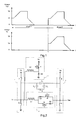
- FIG. 1 shows an example of voltage signals applied on the electrodes Ys and Yas of a display cell during a phase where the electrical charges in the display cells are equalized.
- This equalization phase known as the reset phase, conventionally comprises an operation for forming electrical charges, known as priming, followed by an operation for adjusting the charges, also known as the "erase" of these charges, after which, ideally, the internal voltages within the cells are substantially the same.
- the electrical charges are reset in the discharge regions between coplanar electrodes, called coplanar discharge regions, and in the discharge regions between non-coplanar electrodes, called non-coplanar discharge regions.
- this reset operation is generally carried out first of all in the coplanar discharge regions (phase 1) and then in the non-coplanar discharge regions (phase 2).
- the priming and erase operations are performed by applying a voltage ramp to the electrodes Yas, the potential on the electrodes Ys and on the column electrodes of the PDP (plasma display panel) being held constant. More precisely, the formation of electrical charges in the discharge regions is obtained by applying a rising voltage ramp to the electrodes Yas and the adjustment of the latter is then obtained by applying a falling voltage ramp also to these same electrodes.
- the operation for resetting the electrical charges in the non-coplanar discharge regions (phase 2) consists in applying a rising voltage ramp and then a falling voltage ramp to the electrodes Ys and Yas of the cells.
- a voltage rising edge between zero volts and a voltage Vs is applied simultaneously to the two electrodes Ys and Yas of the cells at the time tl.
- the invention proposes a reduction in the power losses within the device for controlling the PDP during the application of a rising or falling edge to the electrodes Ys and Yas of the PDP cells by using power recovery means already present in the control device.
- the invention also relates to a control device for a plasma display panel designed to generate a voltage rising or falling edge simultaneously on a sustain electrode Ys and on an address-sustain electrode Yas of a cell of the said plasma display panel, the voltage generated going, during the said rising or falling edge, from an initial value to a final value, power recovery means being connected between the said sustain electrode and an address-sustain electrode in order to recover power during the sustain phase of the discharges in the display cells, characterized in that it comprises first means for taking the voltage of one of the said sustain electrode and address-sustain electrode from the initial value to the final value, the said first means cooperating with the power recovery means in order to simultaneously bring the other of the said sustain electrode and address-sustain electrode to the final voltage.
- the use of the power recovery means of the control device allows the use of a second dedicated circuit for applying the final voltage to the other of the said sustain electrode and address-sustain electrode to be eliminated and, at the same time, an additional consumption of power in the device to be avoided.
- the said first means comprise, in the case of a rising edge, a switch and a diode connected in series between a voltage source for supplying the said final voltage value and earth, with the diode anode on the earth side, and an inductor connected, by a first end, to the point situated between the switch and the diode and, by a second end, to one of the said sustain electrode and address-sustain electrode.
- the control device of the invention comprises a circuit 1 for locking the voltages applied to the electrodes Ys and Yas, a power recovery circuit 2 and a means 3 of applying a voltage Vs to the electrode Ys.
- the means 3 cooperates with the power recovery circuit 2 in order to simultaneously apply the voltage from the means 3 to the two cell electrodes Ys and Yas of the plasma display.
- the capacitance between the electrodes Ys and Yas of the panel is represented by the capacitor C 1 in the figure.
- the capacitance between, on the one hand, the electrodes Ys and Yas and, on the other hand, the column electrodes referenced X of the panel is represented in the figure by the capacitors C 2 and C 3 . These capacitances are shown in the figure by dotted line.
- the locking circuit 1 consists of four switches I1, I2, I3 and I4. Two switches, I1 and I2, are connected in series between a power supply terminal receiving the voltage Vs and earth. The mid-point between these two switches is connected to the cell electrodes Ys of the display. The two other switches, I3 and I4, are also connected in series between a power supply terminal receiving the voltage Vs and earth. The mid-point between these two switches is connected to the cell electrodes Yas of the display.
- the means 3 comprises a switch I7 connected in series with a diode D3 between a power supply terminal receiving the voltage Vs and earth.
- the diode D3 is oriented so as to prevent the current through the switch I7 from flowing to earth.
- An inductor L2 is also connected between the point situated between the switch I7 and the diode D3 on the one hand and the sustain electrode Ys on the other.
- the means 3 could, of course, just as well be connected to the address-sustain electrode Yas.
- the power recovery circuit 2 is connected between the electrodes Ys and Yas of the display cells.
- This circuit is, for example, of the type described in the European Patent Application EP 0 704 834. It comprises an inductor L1 connected in series with a two-way switch between the electrodes Ys and Yas.
- the two-way switch is formed by a switch I5 in series with a diode D1 that allows the current to flow in one direction when the switch I5 is closed and by, connected in parallel, a switch I6 connected in series with a diode D2 that allows the current to flow in the opposite direction when the switch I6 is closed.
- the inductor L is connected in parallel with the display capacitance shown by the capacitors C 1 , C 2 and C 3 in the figure 2 and forms a resonant circuit with the latter.
- This power recovery circuit 2 is generally used during the sustain phase of the discharges in the cells. Outside of this phase, the switches I5 and I6 are generally open.
- the switch I5 when it is desired to simultaneously apply a voltage Vs to the electrodes Ys and Yas, the switch I5 is closed in order to transmit the voltage Vs applied to the electrode Ys to the electrode Yas.
- the switches I5 and I7 are closed.
- the switch I5 can even be closed shortly before the switch I7 in order to limit the switching losses in the switch I5.
- a current originating from the supply source of the voltage Vs is now delivered to the inductor L2.
- the current rises progressively in the inductor L2 and is retransmitted to the electrode Ys and, via the switch I5, to the electrode Yas.
- the voltage on the electrodes Ys and Yas therefore rises progressively.
- the voltage rise on the electrode Ys happens shortly before that of the electrode Yas owing to the presence of the inductor L1.
- the switch I7 is opened.
- the voltage across the terminals of the inductor L2 is inverted and the current in the latter starts to decrease.
- the continuity of the current in the inductor L2 is assured by the diode D3.
- This current continues to be delivered to the electrodes Ys and Yas.
- the switch I5 is opened.
- the switches I1 and I3 are then closed and take over from the means 3 in supplying the voltage Vs. This closure of the switches I1 and I3 may indifferently be shortly before, at the same time as, or shortly after that of the switch I5.
- the means 3 could be eliminated and the switch I1 be used to raise the voltage of the electrode Ys.
- this embodiment will result in greater power losses than those of the device in Figure 2. These losses would nevertheless be smaller than those of a device comprising dedicated circuits for raising the voltage of the electrodes Ys and Yas.
Landscapes
- Engineering & Computer Science (AREA)
- Physics & Mathematics (AREA)
- Power Engineering (AREA)
- Plasma & Fusion (AREA)
- Computer Hardware Design (AREA)
- General Physics & Mathematics (AREA)
- Theoretical Computer Science (AREA)
- Control Of Indicators Other Than Cathode Ray Tubes (AREA)
- Control Of Gas Discharge Display Tubes (AREA)
- Transforming Electric Information Into Light Information (AREA)
Applications Claiming Priority (2)
| Application Number | Priority Date | Filing Date | Title |
|---|---|---|---|
| FR0309729A FR2858708A1 (fr) | 2003-08-07 | 2003-08-07 | Dispositif de commande dans un panneau de visualisation au plasma |
| FR0309729 | 2003-08-07 |
Publications (3)
| Publication Number | Publication Date |
|---|---|
| EP1505561A2 true EP1505561A2 (fr) | 2005-02-09 |
| EP1505561A3 EP1505561A3 (fr) | 2008-03-05 |
| EP1505561B1 EP1505561B1 (fr) | 2014-04-16 |
Family
ID=33548319
Family Applications (1)
| Application Number | Title | Priority Date | Filing Date |
|---|---|---|---|
| EP04016406.3A Expired - Lifetime EP1505561B1 (fr) | 2003-08-07 | 2004-07-13 | Dispositif de commande d'un panneau d'affichage plasma |
Country Status (7)
| Country | Link |
|---|---|
| US (1) | US7768479B2 (fr) |
| EP (1) | EP1505561B1 (fr) |
| JP (1) | JP4666973B2 (fr) |
| KR (1) | KR101074037B1 (fr) |
| CN (1) | CN100409285C (fr) |
| FR (1) | FR2858708A1 (fr) |
| TW (1) | TW200506789A (fr) |
Families Citing this family (1)
| Publication number | Priority date | Publication date | Assignee | Title |
|---|---|---|---|---|
| GB201309282D0 (en) * | 2013-05-23 | 2013-07-10 | Shimadzu Corp | Circuit for generating a voltage waveform |
Citations (1)
| Publication number | Priority date | Publication date | Assignee | Title |
|---|---|---|---|---|
| EP0704834A1 (fr) | 1994-09-28 | 1996-04-03 | Nec Corporation | Circuit d'entraînement pour dispositif d'affichage à plasma du type mémoire |
Family Cites Families (13)
| Publication number | Priority date | Publication date | Assignee | Title |
|---|---|---|---|---|
| US5227696A (en) * | 1992-04-28 | 1993-07-13 | Westinghouse Electric Corp. | Power saver circuit for TFEL edge emitter device |
| US5642018A (en) * | 1995-11-29 | 1997-06-24 | Plasmaco, Inc. | Display panel sustain circuit enabling precise control of energy recovery |
| JP2976923B2 (ja) * | 1997-04-25 | 1999-11-10 | 日本電気株式会社 | 容量性負荷の駆動装置 |
| KR100295455B1 (ko) * | 1999-06-15 | 2001-07-12 | 구자홍 | 플라즈마 디스플레이 패널의 전압분리 구동방법 및 장치 |
| WO2001088893A1 (fr) * | 2000-05-16 | 2001-11-22 | Koninklijke Philips Electronics N.V. | Circuit d'attaque a recuperation d'energie pour afficheur a ecran plat |
| TW526459B (en) * | 2000-06-23 | 2003-04-01 | Au Optronics Corp | Plasma display holding-stage driving circuit with discharging current compensation function |
| KR20030003564A (ko) * | 2001-07-03 | 2003-01-10 | 주식회사 유피디 | 교류형 플라즈마 디스플레이 패널의 유지 구동 장치의에너지 회수 회로 |
| US7317454B2 (en) * | 2001-08-08 | 2008-01-08 | Lg Electronics, Inc. | Energy recovery circuit of display device |
| CN100369082C (zh) * | 2001-10-16 | 2008-02-13 | 三星Sdi株式会社 | 驱动等离子显示屏的设备及其方法 |
| US6850213B2 (en) * | 2001-11-09 | 2005-02-01 | Matsushita Electric Industrial Co., Ltd. | Energy recovery circuit for driving a capacitive load |
| JP2003330411A (ja) * | 2002-05-03 | 2003-11-19 | Lg Electronics Inc | プラズマディスプレイパネルの駆動方法及び装置 |
| KR100490614B1 (ko) * | 2002-05-14 | 2005-05-17 | 삼성에스디아이 주식회사 | 플라즈마 디스플레이 패널의 구동 장치 및 그 구동 방법 |
| KR100497230B1 (ko) * | 2002-07-23 | 2005-06-23 | 삼성에스디아이 주식회사 | 플라즈마 디스플레이 패널의 구동 장치 및 구동 방법 |
-
2003
- 2003-08-07 FR FR0309729A patent/FR2858708A1/fr active Pending
-
2004
- 2004-07-13 EP EP04016406.3A patent/EP1505561B1/fr not_active Expired - Lifetime
- 2004-08-03 JP JP2004227136A patent/JP4666973B2/ja not_active Expired - Fee Related
- 2004-08-04 KR KR1020040061264A patent/KR101074037B1/ko not_active Expired - Fee Related
- 2004-08-06 CN CNB200410068413XA patent/CN100409285C/zh not_active Expired - Fee Related
- 2004-08-06 US US10/912,791 patent/US7768479B2/en not_active Expired - Fee Related
- 2004-08-06 TW TW093123564A patent/TW200506789A/zh unknown
Patent Citations (1)
| Publication number | Priority date | Publication date | Assignee | Title |
|---|---|---|---|---|
| EP0704834A1 (fr) | 1994-09-28 | 1996-04-03 | Nec Corporation | Circuit d'entraînement pour dispositif d'affichage à plasma du type mémoire |
Also Published As
| Publication number | Publication date |
|---|---|
| KR20050016121A (ko) | 2005-02-21 |
| EP1505561A3 (fr) | 2008-03-05 |
| US20050030262A1 (en) | 2005-02-10 |
| CN100409285C (zh) | 2008-08-06 |
| CN1581265A (zh) | 2005-02-16 |
| KR101074037B1 (ko) | 2011-10-17 |
| TW200506789A (en) | 2005-02-16 |
| JP4666973B2 (ja) | 2011-04-06 |
| FR2858708A1 (fr) | 2005-02-11 |
| JP2005055905A (ja) | 2005-03-03 |
| EP1505561B1 (fr) | 2014-04-16 |
| US7768479B2 (en) | 2010-08-03 |
Similar Documents
| Publication | Publication Date | Title |
|---|---|---|
| US6583575B2 (en) | Energy recovery sustain circuit for AC plasma display panel | |
| US7382338B2 (en) | Driver circuit for plasma display panels | |
| US7078866B2 (en) | Plasma display panel and method for driving the same | |
| US6903515B2 (en) | Sustain driving apparatus and method for plasma display panel | |
| TW473700B (en) | Data line drive device | |
| US7768479B2 (en) | Control device in a plasma display panel | |
| JP2006058855A (ja) | プラズマディスプレイパネルとその駆動方法 | |
| US7355350B2 (en) | Apparatus for energy recovery of a plasma display panel | |
| US7605781B2 (en) | Display panel driving method | |
| US7064732B2 (en) | Method of controlling a circuit arrangement for the ac power supply of a plasma display panel | |
| US20060050020A1 (en) | Plasma display apparatus and driving method thereof | |
| US7327334B2 (en) | Plasma display panel driver circuit having two-direction energy recovery through one switch | |
| US8410998B2 (en) | Device for driving a plasma display panel | |
| JP2000163012A (ja) | 表示パネルの駆動方式 | |
| US7348941B2 (en) | Driving circuit of plasma display panel | |
| US20070040766A1 (en) | Plasma display panel power recovery method and apparatus | |
| US7609233B2 (en) | Plasma display device and driving apparatus thereof | |
| US20070247396A1 (en) | Plasma display apparatus and driving method thereof | |
| WO1982002314A1 (fr) | Dispositif de transfert de charge a plasma | |
| KR100676756B1 (ko) | 플라즈마 디스플레이 패널의 집적된 어드레스 구동 회로모듈, 구동 장치 및 구동방법 | |
| EP1780691A1 (fr) | Appareil et procédé de commande pour un panneau d'affichage à plasma | |
| US20070091017A1 (en) | Plasma display driving method and apparatus | |
| CN100589161C (zh) | 驱动等离子显示装置的方法 | |
| KR100764662B1 (ko) | 플라즈마 디스플레이 장치 및 그 구동방법 | |
| US20070091026A1 (en) | Plasma display device and driving method thereof |
Legal Events
| Date | Code | Title | Description |
|---|---|---|---|
| PUAI | Public reference made under article 153(3) epc to a published international application that has entered the european phase |
Free format text: ORIGINAL CODE: 0009012 |
|
| AK | Designated contracting states |
Kind code of ref document: A2 Designated state(s): AT BE BG CH CY CZ DE DK EE ES FI FR GB GR HU IE IT LI LU MC NL PL PT RO SE SI SK TR |
|
| AX | Request for extension of the european patent |
Extension state: AL HR LT LV MK |
|
| RAP1 | Party data changed (applicant data changed or rights of an application transferred) |
Owner name: THOMSON LICENSING |
|
| PUAL | Search report despatched |
Free format text: ORIGINAL CODE: 0009013 |
|
| AK | Designated contracting states |
Kind code of ref document: A3 Designated state(s): AT BE BG CH CY CZ DE DK EE ES FI FR GB GR HU IE IT LI LU MC NL PL PT RO SE SI SK TR |
|
| AX | Request for extension of the european patent |
Extension state: AL HR LT LV MK |
|
| 17P | Request for examination filed |
Effective date: 20080905 |
|
| AKX | Designation fees paid |
Designated state(s): DE FR GB |
|
| RAP1 | Party data changed (applicant data changed or rights of an application transferred) |
Owner name: THOMSON LICENSING |
|
| 17Q | First examination report despatched |
Effective date: 20110331 |
|
| RIC1 | Information provided on ipc code assigned before grant |
Ipc: G09G 3/288 20060101AFI20120119BHEP |
|
| REG | Reference to a national code |
Ref country code: DE Ref legal event code: R079 Ref document number: 602004044822 Country of ref document: DE Free format text: PREVIOUS MAIN CLASS: G09G0003280000 Ipc: G09G0003288000 |
|
| RIC1 | Information provided on ipc code assigned before grant |
Ipc: G09G 3/296 20130101ALN20130924BHEP Ipc: G09G 3/292 20130101ALN20130924BHEP Ipc: G09G 3/288 20130101AFI20130924BHEP |
|
| GRAP | Despatch of communication of intention to grant a patent |
Free format text: ORIGINAL CODE: EPIDOSNIGR1 |
|
| RIC1 | Information provided on ipc code assigned before grant |
Ipc: G09G 3/288 20130101AFI20130930BHEP Ipc: G09G 3/292 20130101ALN20130930BHEP Ipc: G09G 3/296 20130101ALN20130930BHEP |
|
| RIC1 | Information provided on ipc code assigned before grant |
Ipc: G09G 3/288 20130101AFI20131010BHEP Ipc: G09G 3/292 20130101ALN20131010BHEP Ipc: G09G 3/296 20130101ALN20131010BHEP |
|
| INTG | Intention to grant announced |
Effective date: 20131104 |
|
| RIC1 | Information provided on ipc code assigned before grant |
Ipc: G09G 3/288 20130101AFI20131021BHEP Ipc: G09G 3/292 20130101ALN20131021BHEP Ipc: G09G 3/296 20130101ALN20131021BHEP |
|
| GRAS | Grant fee paid |
Free format text: ORIGINAL CODE: EPIDOSNIGR3 |
|
| GRAA | (expected) grant |
Free format text: ORIGINAL CODE: 0009210 |
|
| AK | Designated contracting states |
Kind code of ref document: B1 Designated state(s): DE FR GB |
|
| REG | Reference to a national code |
Ref country code: GB Ref legal event code: FG4D |
|
| REG | Reference to a national code |
Ref country code: DE Ref legal event code: R096 Ref document number: 602004044822 Country of ref document: DE Effective date: 20140528 |
|
| REG | Reference to a national code |
Ref country code: DE Ref legal event code: R084 Ref document number: 602004044822 Country of ref document: DE Effective date: 20140425 |
|
| PGFP | Annual fee paid to national office [announced via postgrant information from national office to epo] |
Ref country code: DE Payment date: 20140724 Year of fee payment: 11 |
|
| PGFP | Annual fee paid to national office [announced via postgrant information from national office to epo] |
Ref country code: FR Payment date: 20140702 Year of fee payment: 11 |
|
| REG | Reference to a national code |
Ref country code: DE Ref legal event code: R097 Ref document number: 602004044822 Country of ref document: DE |
|
| PLBE | No opposition filed within time limit |
Free format text: ORIGINAL CODE: 0009261 |
|
| STAA | Information on the status of an ep patent application or granted ep patent |
Free format text: STATUS: NO OPPOSITION FILED WITHIN TIME LIMIT |
|
| 26N | No opposition filed |
Effective date: 20150119 |
|
| GBPC | Gb: european patent ceased through non-payment of renewal fee |
Effective date: 20140716 |
|
| REG | Reference to a national code |
Ref country code: DE Ref legal event code: R097 Ref document number: 602004044822 Country of ref document: DE Effective date: 20150119 |
|
| PG25 | Lapsed in a contracting state [announced via postgrant information from national office to epo] |
Ref country code: GB Free format text: LAPSE BECAUSE OF NON-PAYMENT OF DUE FEES Effective date: 20140716 |
|
| REG | Reference to a national code |
Ref country code: DE Ref legal event code: R119 Ref document number: 602004044822 Country of ref document: DE |
|
| PG25 | Lapsed in a contracting state [announced via postgrant information from national office to epo] |
Ref country code: DE Free format text: LAPSE BECAUSE OF NON-PAYMENT OF DUE FEES Effective date: 20160202 |
|
| REG | Reference to a national code |
Ref country code: FR Ref legal event code: ST Effective date: 20160331 |
|
| PG25 | Lapsed in a contracting state [announced via postgrant information from national office to epo] |
Ref country code: FR Free format text: LAPSE BECAUSE OF NON-PAYMENT OF DUE FEES Effective date: 20150731 |