EP1505698B1 - Halbleitervorrichtung mit Übergitter und Herstellungsverfahren - Google Patents
Halbleitervorrichtung mit Übergitter und Herstellungsverfahren Download PDFInfo
- Publication number
- EP1505698B1 EP1505698B1 EP04253951A EP04253951A EP1505698B1 EP 1505698 B1 EP1505698 B1 EP 1505698B1 EP 04253951 A EP04253951 A EP 04253951A EP 04253951 A EP04253951 A EP 04253951A EP 1505698 B1 EP1505698 B1 EP 1505698B1
- Authority
- EP
- European Patent Office
- Prior art keywords
- layer
- material layers
- holes
- layers
- superlattice
- Prior art date
- Legal status (The legal status is an assumption and is not a legal conclusion. Google has not performed a legal analysis and makes no representation as to the accuracy of the status listed.)
- Expired - Lifetime
Links
Images




Classifications
-
- H—ELECTRICITY
- H01—ELECTRIC ELEMENTS
- H01S—DEVICES USING THE PROCESS OF LIGHT AMPLIFICATION BY STIMULATED EMISSION OF RADIATION [LASER] TO AMPLIFY OR GENERATE LIGHT; DEVICES USING STIMULATED EMISSION OF ELECTROMAGNETIC RADIATION IN WAVE RANGES OTHER THAN OPTICAL
- H01S3/00—Lasers, i.e. devices using stimulated emission of electromagnetic radiation in the infrared, visible or ultraviolet wave range
- H01S3/09—Processes or apparatus for excitation, e.g. pumping
- H01S3/091—Processes or apparatus for excitation, e.g. pumping using optical pumping
- H01S3/094—Processes or apparatus for excitation, e.g. pumping using optical pumping by coherent light
- H01S3/0941—Processes or apparatus for excitation, e.g. pumping using optical pumping by coherent light of a laser diode
-
- H—ELECTRICITY
- H10—SEMICONDUCTOR DEVICES; ELECTRIC SOLID-STATE DEVICES NOT OTHERWISE PROVIDED FOR
- H10H—INORGANIC LIGHT-EMITTING SEMICONDUCTOR DEVICES HAVING POTENTIAL BARRIERS
- H10H20/00—Individual inorganic light-emitting semiconductor devices having potential barriers, e.g. light-emitting diodes [LED]
- H10H20/80—Constructional details
- H10H20/81—Bodies
- H10H20/811—Bodies having quantum effect structures or superlattices, e.g. tunnel junctions
-
- B—PERFORMING OPERATIONS; TRANSPORTING
- B82—NANOTECHNOLOGY
- B82Y—SPECIFIC USES OR APPLICATIONS OF NANOSTRUCTURES; MEASUREMENT OR ANALYSIS OF NANOSTRUCTURES; MANUFACTURE OR TREATMENT OF NANOSTRUCTURES
- B82Y20/00—Nanooptics, e.g. quantum optics or photonic crystals
-
- H—ELECTRICITY
- H10—SEMICONDUCTOR DEVICES; ELECTRIC SOLID-STATE DEVICES NOT OTHERWISE PROVIDED FOR
- H10D—INORGANIC ELECTRIC SEMICONDUCTOR DEVICES
- H10D62/00—Semiconductor bodies, or regions thereof, of devices having potential barriers
- H10D62/80—Semiconductor bodies, or regions thereof, of devices having potential barriers characterised by the materials
- H10D62/81—Semiconductor bodies, or regions thereof, of devices having potential barriers characterised by the materials of structures exhibiting quantum-confinement effects, e.g. single quantum wells; of structures having periodic or quasi-periodic potential variation
- H10D62/815—Semiconductor bodies, or regions thereof, of devices having potential barriers characterised by the materials of structures exhibiting quantum-confinement effects, e.g. single quantum wells; of structures having periodic or quasi-periodic potential variation of structures having periodic or quasi-periodic potential variation, e.g. superlattices or multiple quantum wells [MQW]
- H10D62/8161—Semiconductor bodies, or regions thereof, of devices having potential barriers characterised by the materials of structures exhibiting quantum-confinement effects, e.g. single quantum wells; of structures having periodic or quasi-periodic potential variation of structures having periodic or quasi-periodic potential variation, e.g. superlattices or multiple quantum wells [MQW] potential variation due to variations in composition or crystallinity, e.g. heterojunction superlattices
- H10D62/8162—Semiconductor bodies, or regions thereof, of devices having potential barriers characterised by the materials of structures exhibiting quantum-confinement effects, e.g. single quantum wells; of structures having periodic or quasi-periodic potential variation of structures having periodic or quasi-periodic potential variation, e.g. superlattices or multiple quantum wells [MQW] potential variation due to variations in composition or crystallinity, e.g. heterojunction superlattices having quantum effects only in the vertical direction, i.e. layered structures having quantum effects solely resulting from vertical potential variation
- H10D62/8164—Semiconductor bodies, or regions thereof, of devices having potential barriers characterised by the materials of structures exhibiting quantum-confinement effects, e.g. single quantum wells; of structures having periodic or quasi-periodic potential variation of structures having periodic or quasi-periodic potential variation, e.g. superlattices or multiple quantum wells [MQW] potential variation due to variations in composition or crystallinity, e.g. heterojunction superlattices having quantum effects only in the vertical direction, i.e. layered structures having quantum effects solely resulting from vertical potential variation comprising only semiconductor materials
-
- B—PERFORMING OPERATIONS; TRANSPORTING
- B82—NANOTECHNOLOGY
- B82Y—SPECIFIC USES OR APPLICATIONS OF NANOSTRUCTURES; MEASUREMENT OR ANALYSIS OF NANOSTRUCTURES; MANUFACTURE OR TREATMENT OF NANOSTRUCTURES
- B82Y40/00—Manufacture or treatment of nanostructures
-
- H—ELECTRICITY
- H01—ELECTRIC ELEMENTS
- H01S—DEVICES USING THE PROCESS OF LIGHT AMPLIFICATION BY STIMULATED EMISSION OF RADIATION [LASER] TO AMPLIFY OR GENERATE LIGHT; DEVICES USING STIMULATED EMISSION OF ELECTROMAGNETIC RADIATION IN WAVE RANGES OTHER THAN OPTICAL
- H01S2301/00—Functional characteristics
- H01S2301/17—Semiconductor lasers comprising special layers
- H01S2301/173—The laser chip comprising special buffer layers, e.g. dislocation prevention or reduction
-
- H—ELECTRICITY
- H10—SEMICONDUCTOR DEVICES; ELECTRIC SOLID-STATE DEVICES NOT OTHERWISE PROVIDED FOR
- H10D—INORGANIC ELECTRIC SEMICONDUCTOR DEVICES
- H10D62/00—Semiconductor bodies, or regions thereof, of devices having potential barriers
- H10D62/80—Semiconductor bodies, or regions thereof, of devices having potential barriers characterised by the materials
- H10D62/85—Semiconductor bodies, or regions thereof, of devices having potential barriers characterised by the materials being Group III-V materials, e.g. GaAs
- H10D62/8503—Nitride Group III-V materials, e.g. AlN or GaN
-
- H—ELECTRICITY
- H10—SEMICONDUCTOR DEVICES; ELECTRIC SOLID-STATE DEVICES NOT OTHERWISE PROVIDED FOR
- H10H—INORGANIC LIGHT-EMITTING SEMICONDUCTOR DEVICES HAVING POTENTIAL BARRIERS
- H10H20/00—Individual inorganic light-emitting semiconductor devices having potential barriers, e.g. light-emitting diodes [LED]
- H10H20/80—Constructional details
- H10H20/81—Bodies
- H10H20/811—Bodies having quantum effect structures or superlattices, e.g. tunnel junctions
- H10H20/812—Bodies having quantum effect structures or superlattices, e.g. tunnel junctions within the light-emitting regions, e.g. having quantum confinement structures
-
- H—ELECTRICITY
- H10—SEMICONDUCTOR DEVICES; ELECTRIC SOLID-STATE DEVICES NOT OTHERWISE PROVIDED FOR
- H10H—INORGANIC LIGHT-EMITTING SEMICONDUCTOR DEVICES HAVING POTENTIAL BARRIERS
- H10H20/00—Individual inorganic light-emitting semiconductor devices having potential barriers, e.g. light-emitting diodes [LED]
- H10H20/80—Constructional details
- H10H20/81—Bodies
- H10H20/822—Materials of the light-emitting regions
- H10H20/824—Materials of the light-emitting regions comprising only Group III-V materials, e.g. GaP
- H10H20/825—Materials of the light-emitting regions comprising only Group III-V materials, e.g. GaP containing nitrogen, e.g. GaN
Definitions
- the present invention relates to a semiconductor having a superlattice semiconductor layer and a method of manufacturing the same, and more particularly, to a semiconductor device having a GaN superlattice semiconductor layer for reducing a driving voltage by decreasing a series resistance and a method of manufacturing the same.
- a laser diode has a superlattice structure in which different materials are stacked to form a multi-layer.
- a GaN based LD has a superlattice structure in which AlGaN and GaN are stacked in a sandwich structure as shown in FIG. 1 .
- Such a GaN based LD requires AlGaN having a large amount of Al in order to improve an optical confinement.
- AlGaN having a large amount of Al increases a series resistance of the LD that causes an increase in a driving voltage of the LD.
- the increase in the driving voltage of the LD reduces the lifespan of the LD.
- a GaN based material is studied to be applied to an optical device field, such as a light emitting diode (LED) and an LD. Decreases in an oscillation current and a driving voltage reduce an input power to an LD, resulting in the improvement of durability. Since Mg as a p-type dopant has a low doping efficiency, an increase in the driving voltage usually occurs in a p-type layer. Referring to the Japanese Laid-open Patent No. 13-308458 and the Japanese Laid-open Patent No.
- p-type layers in a GaN based LD include a p-GaN optical waveguide layer, a p-AlGaN/GaN optical confinement layer, and a p-GaN contact layer.
- An optical confinement layer has a superlattice structure having a GaN layer interposed between AlGaN layers.
- the GaN layer interposed between the AlGaN layers in the optical confinement layer prevents cracks of the AlGaN layers having a large amount of Al.
- the superlattice structure having GaN and AlGaN increases a doping efficiency of a deep acceptor by forming two dimensional hole gas and increases a hole concentration by increasing the doping efficiency as well as generating a higher doping efficiency than a bulk AlGaN layer.
- the series resistance should be reduced to increase the lifespan of the LD, so the amount of Al should be reduced to reduce the resistance of the superlattice structure.
- the amount of Al since the reduction of the amount of Al deteriorates the optical confinement, there is a limit of reducing the amount of Al.
- a laser diode (LD) according to claim 4.
- the present invention provides a semiconductor device having a superlattice semiconductor layer for reducing a series resistance without decrease in an optical confinement and a method of manufacturing the same.
- the present invention provides a semiconductor device having a superlattice semiconductor layer with a reduced input power due to a reduced series resistance and an improved durability and a method of manufacturing the same.
- FIG. 1 is a sectional view illustrating a semiconductor laser diode (LD) according to the present invention.
- a semiconductor LD according to the present invention includes a substrate 50 and a first semiconductor layer 61, a laser resonance layer 62, and a second semiconductor layer 63, which are grown on the substrate 50.
- the first semiconductor layer 61 as a lower material layer includes a buffer layer 52, which is grown on the substrate 50, and a lower cladding layer 54 stacked on the buffer layer 52.
- a sapphire substrate or a free-standing gallium nitride (GaN) substrate is used for the substrate 50.
- the buffer layer 52 is an n-GaN based group III-V nitride compound semiconductor layer, and it is preferable that the buffer layer 52 is an n-GaN layer.
- the buffer layer 52 may be another group III-V compound semiconductor layer that can oscillate laser, in other words, lasing.
- the lower cladding layer 54 is an n-GaN/AlGaN superlattice structure layer having a predetermined refractive index, but can be formed of another compound that can oscillate laser.
- the resonance layer 63 includes a lower wave guide layer 53, an active layer 56, and an upper wave guide layer 55, which are sequentially stacked on the lower cladding layer 54.
- the upper and lower wave guide layers 55 and 53 are formed of a material having a smaller refractive index than the active layer 56. It is preferable that the upper and lower wave guide layers 55 and 53 are GaN based group III-V compound semiconductor layers.
- the lower wave guide layer 53 is an n-GaN layer
- the upper wave guide layer 55 is a p-GaN layer.
- the active layer 56 is formed of a lasing material, preferably a material for oscillating a laser beam which has a small critical current and a stable traverse mode characteristic.
- the active layer 56 may have a multi-quantum well structure or a single quantum well structure, and the structure of the active layer 56 does not limit the scope of the present invention.
- the second semiconductor layer 65 as an upper material layer is stacked on the upper surface of the upper wave guide layer 55.
- a ridge 58a is formed on the upper material layer to form a ridge waveguide. Since the ridge structure is widely known, the description of the ridge structure will be omitted.
- the second semiconductor layer 65 includes an upper cladding layer 58 having a smaller refractive index than the upper wave guide layer 55, and an ohmic contact layer 64 stacked on the upper surface of the upper cladding layer 58.
- the upper cladding layer 58 is a p-type compound semiconductor layer.
- the upper cladding layer 58 is an n-type compound semiconductor layer.
- the lower cladding layer 54 is the n-GaN/AlGaN layer
- the upper cladding layer 58 is a p-GaN/AlGaN layer.
- the ohmic contact layer 64 is a p-type compound semiconductor layer, and when the buffer layer 52 is formed of n-GaN, the ohmic contact layer 64 is formed of p-GaN.
- a buried layer 68 as a passivation layer covers upper edges of the upper cladding layer 58 and the ridge 58a protruded at the center of the upper cladding layer 58.
- a protective layer 69 is formed on the upper surface of the buried layer 68 to cover the buried layer 68.
- the buried layer 68 is formed of a conventional passivation material, for example, an oxide including at least one element selected from a group formed of Si, Al, Zr, and Ta.
- the protective layer 69 is formed of a material having excellent etch selectivity and adherence to the passivation material, for example, Cr or TiO 2 .
- the protective layer 69 operates as a protective mask when etching the buried layer 68.
- a p-type upper electrode 57 is formed on the top of the ridge wave guide structure having the buried layer 68 and the protective layer 69. The central portion of the upper electrode 57 contacts the ohmic contact layer 64 at the top of the ridge 58a, and the edges of the upper electrode 57 extend to the edges of the upper cladding layer 58.
- FIG. 2 is a perspective view illustrating the stacked structure of the p-cladding layer
- FIG. 3 is a sectional view illustrating the stacked structure of a superlattice layer in a conventional LD.
- first layers 581 and second layers 582 are alternately stacked and a plurality of holes 581 a and 582a are formed in each layer, respectively.
- a plurality of holes 581 a and 582a are formed in the AlGaN first layers 581 and p-doped GaN second layers 582, respectively.
- the holes 581 a and 582a are filled with the materials of the adjacent layers.
- the holes 581 a of the first layers 581 are filled with the second layer material
- the holes 582a of the second layers 582 are filled with the first layer material.
- the same material layers that are separated by the structure in which different material layers are alternately stacked are connected through the holes formed between the same material layers.
- the AlGaN layers having a lower resistance than the GaN second layers 582 are connected to each other, thereby reducing an electric resistance compared to a structure in which AlGaN layers are entirely connected in the superlattice structure.
- the number of the holes 581 a and 582a is large, and the size of the holes 581 a and 582a is in a range from nanmeters to microns.
- the present invention is provided to reduce a resistance in a superlattice structure, such as a p-cladding layer, which is realized by forming the holes having a size of microns to nanometers in the material layers.
- the holes connect the same material layers, resulting in the reduction of the driving voltage of an LD device.
- a driving voltage is reduced by about 1 V when a superlattice having the nano-holes is applied to an LD in an experiment. By reducing the driving voltage, an input power is reduced and the heat from the device is easily discharged, resulting in the increase in the lifespan of the LD.
- Characteristic tests are performed on specimens that are manufactured by a conventional method and the present invention to which a superlattice having nano-holes is applied.
- an FWHM value is very sharp at 100 to 250 arcsec.
- Such an interface operates as a barrier to increase the resistance of a device resulting in the increases in a driving voltage and an input power so that the lifespan of the device is reduced.
- FIGS. 4A and 4B are graphs illustrating (0002) 2 ⁇ - ⁇ scanning results of LD specimens to which a conventional superlattice structure and a superlattice according to the present invention are applied, respectively.
- the graphs of FIGS. 4A and 4B illustrate similar results, particularly, AlGaN 0 th peaks are the same in the graphs, which means that the compositions of Al included in the LD specimens are the same. Accordingly, it is predicted that the optical confinements of the specimens are the same.
- the intensity and the FWHM of AlGaN -1 st peak of the specimen according to the present invention is twice larger than those of the specimen manufactured by the conventional method, which means that the interface between the AlGaN layer and the GaN layer in the superlattice is uneven.
- FIG. 5 is a TEM image of a specimen having a conventional superlattice structure.
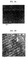
- FIG. 6A is a TEM image of a specimen having a superlattice structure including nano-holes according to the present invention, and
- FIG. 6B is an enlarged image of the square of FIG. 6A .
- Bright potions of the TEM images of FIGS. 5 through 6B denote AlGaN regions, and dark portions of the TEM images of FIGS. 5 through 6B denote GaN regions.
- the interfaces between the AlGaN regions and the GaN regions are clearly divided.
- the interfaces between the AlGaN regions and the GaN regions in the superlattice according to the present invention cannot be easily distinguished.
- nano-holes are formed in interlayer between AlGaN and GaN and interlayer between GaN and AlGaN to vertically connect the same material layers. Arrows in FIG.
- the doped GaN regions progress along the nano-holes, which are vertically connected.
- the nano-holes of AlGaN and GaN are vertically formed over a large area.
- the holes are transferred to the active layer, the holes are likely transferred through the nano-holes than through the barriers.
- the series resistance of the LD decreases.
- FIGS. 7A and 7B are graphs illustrating the series resistances and the voltages at 50 mA of the specimens to which a conventional superlattice obtained under a pressure of 13.3 kPa (100 Torr) and a nano-hole superlattice obtained under a pressure of 26.7 kPa (200 Torr) are applied.
- the specimen having the nano-hole superlattice according to the present invention has a series resistance about half of the series resistance of the conventional specimen.
- the voltage at 50 mA of the specimen according to the present invention is reduced by about 1V in each cavity length. Accordingly, it is known that the nano-holes can be formed in the superlattice by controlling the pressure when growing the superlattice.
- a growing pressure is increased while growing crystals.
- the growing pressure is increased, desorption is increased from a growing layer and incorporation of Al and Ga is reduced, resulting in an uneven growing of a AlGaN layer or a GaN layer at the interface.
- fine hollow areas are formed in the AlGaN layer and the GaN layer in a lateral direction.
- nano-holes in other words, nano-channels through which the AlGaN layer and the AlGaN layer, and the GaN layer and the GaN layer are connected.
- the pressure of a reactor is from 20 kPa (150 Torr) to a normal pressure, most preferably 20 kPa to 53 kPa (150 to 400 Torr).
- a growing stop period is provided while growing AlGaN and GaN layers.
- NH 3 and H 2 are supplied to a reactor.
- in-situ etching occurs by H 2 to partially etch a grown crystal layer, resulting in the formation of nano-holes.
- the growing stop period is 3 to 50 seconds, preferably, 3 to 15 seconds.
- a growing speed range for forming nano-holes is 0.1 to 1 nm/s (1 to 10 ⁇ /s), preferably, 0.2 to 0.6 nm/s (2 to 6 ⁇ /s).
- a first material layer (AlGaN) having a plurality of nano-holes is formed on a lower material layer, for example, a p-type wave guide layer (WGL) of an LD.
- the first material layer (AlGaN) having a plurality of nano-holes is formed by any one method of the above-described methods.
- a second material layer (GaN) having nano-holes is formed on the first material layer (AlGaN).
- the material of the second material layer (GaN) fills the nano-holes of the first material layer (AlGaN).
- a first material layer (AlGaN) is formed on the second material layer (GaN).
- the material of the first material layer (AlGaN) fills the nano-holes of the second material layer (GaN).
- a second material layer (GaN) is formed on the first material layer (AlGaN).
- the material of the second material layer (GaN) fills the nano-holes of the first material layer (AlGaN).
- the second material layers on and under the first material layer are connected through the nano-holes formed in the first material layer, resulting in connecting the same material through the layers.
- a superlattice according to the present invention can be applied to a cladding layer of an LD, and any superlattice structure requiring an optical confinement and a low series resistance. Since a series resistance increases in a p-type layer of an LD, it is preferable that the superlattice according to the present invention is applied to a p-type structure of the LD. However, the superlattice according to the present invention can be applied to an n-type layer. Since electrons flow through an n-type layer, the electrons can be induced to a resonance layer through the nano-holes while not through a barrier between interfaces having a high resistance.
- the superlattice according to the present invention can be applied to not only AlGaN/GaN, but also to nitride materials.
- the superlattice according to the present invention can be applied to Al x In y Ga 1-x-y N/Al x' In y' Ga 1-x'-y' N where 0 ⁇ x, x', y, and y' ⁇ 1, because the superlattice can reduce a resistance by a barrier due to an energy-band gap.
- the superlattice according to the present invention can be applied to regardless of the type of dopants, for example, an n-type, such as Si, or a p-type, such as mg.
- doping may be performed on the both sides of Al x In y Ga 1-x-y N/Al x' In y' Ga 1-x'-y' N layer or on any one side of the layer.
- FIG. 9 is a sectional view illustrating a resultant structure on which a ridge wave guide is not formed yet. Since growing processes of crystal layers on a substrate are repeated and changes in profiles without an increase in the number of stacked layers do not take place, the method of fabricating an LD is described with reference to FIG. 9 .
- n-GaN contact layer 52 is grown on a surface of an ELOG, GaN, or sapphire substrate 50 in MOCVD equipment.
- the n-GaN contact layer 52 is grown to a thickness of 0.5 ⁇ m at a temperature of 1030°C by using TMG and ammonia as source gases and SiH 4 gas as a dopant gas.
- An n-cladding layer 54 is formed in a conventional superlattice structure or in a superlattice structure having nano-holes at the same temperature of growing the n-GaN contact layer 52.
- An n-GaN wave guide layer 53 is grown to a thickness of 0.1 ⁇ m at the same temperature of growing the n-GaN contact layer 52 by using TMG, ammonia, and SiH 4 as source gases.
- a phase matching layer formed of n-In 0.02 Ga 0.98 N is grown to a thickness of 28 nm (280 ⁇ ) at a temperature of 870°C by using TMI, TMG, and ammonia as source gases and SiH 4 gas as a dopant gas, and a barrier layer formed of n-In 0.02 Ga 0.98 N is formed to a thickness of 100 ⁇ . Accordingly, the phase matching layer formed of the same material as the barrier layer becomes a portion of the barrier layer.
- a well layer formed of In 0.08 Ga 0.92 N is grown to a thickness of 40 ⁇ by using TMI, TMG, and ammonia as source gases while not supplying SiH 4 gas.
- TMI titanium dioxide
- TMG titanium dioxide
- ammonia as source gases while not supplying SiH 4 gas.
- MQW multi quantum well
- a diffusion barrier layer formed of In 0.02 Ga 0.98 N is grown on the MQW 56 to a thickness of 280 ⁇ .
- a multi-quantum barrier (MQB) 55a is grown to a thickness of 200 ⁇ by alternately stacking an AlGaN layer and a p-GaN layer at a temperature of 1030°C and by using TMA, TMG, and ammonia as source gases and Cp 2 Mg as a dopant gas.
- MQB multi-quantum barrier
- a p-GaN wave guide layer 55 is formed to a thickness of 0.1 ⁇ m by using TMG and ammonia as source gases and Cp 2 Mg as a dopant gas.
- a p-cladding layer 58 is grown in an AlGaN/p-GaN superlattice structure having nano-holes.
- a p-contact layer 64 is grown on the p-cladding layer 58 to a thickness of 300 ⁇ by using TMG, ammonia, and Cp 2 Mg.
- a crystal surface is etched in a resonance direction of a laser and a current path is defined in a passivation layer, resulting in a ridge structure.
- an n-type electrode is formed on an upper surface of the n-GaN layer, and a p-type electrode is formed on the ridge to manufacture an LD.
- a flip-chip bonding method for easily discharging heat from a GaN semiconductor LD is performed.
- an LD having an excellent optical confinement characteristic and a low driving voltage can be obtained by efficiently transferring charges through nano-holes while maintaining the optical confinement characteristic in a superlattice structure.
- Such an LD can solve the problems of the driving voltage and the optical confinement when growing an AlGaN/GaN superlattice structure. Accordingly, the superlattice structure according to the present invention can be applied to a light emitting device (LED) and an LD. In addition, an input power is reduced when driving a device using the superlattice structure according to the present invention, resulting in the increase in the lifespan of the device.
- LED light emitting device
Landscapes
- Engineering & Computer Science (AREA)
- Nanotechnology (AREA)
- Physics & Mathematics (AREA)
- Chemical & Material Sciences (AREA)
- Optics & Photonics (AREA)
- Crystallography & Structural Chemistry (AREA)
- Biophysics (AREA)
- Life Sciences & Earth Sciences (AREA)
- Electromagnetism (AREA)
- Plasma & Fusion (AREA)
- Semiconductor Lasers (AREA)
- Led Devices (AREA)
- Light Receiving Elements (AREA)
- Recrystallisation Techniques (AREA)
- Photovoltaic Devices (AREA)
Claims (13)
- Eine optische Halbleitervorrichtung, die eine Supergitter-Halbleiterstruktur aufweist, in welcher Schichten (581) eines ersten Materials (581), die aus einem ersten Material gebildet sind, und Schichten (582) eines zweiten Materials, die aus einem zweiten Material gebildet sind, abwechselnd gestapelt sind, wobei das erste und das zweite Material voneinander unterschiedlich sind, dadurch gekennzeichnet, dass
die Schichten (581) des ersten Materials und die Schichten (582) des zweiten Materials in der aus den Schichten (581) des ersten Materials und den Schichten (582) des zweiten Materials gebildeten Supergitter-Struktur eine Vielzahl von Nano-Löchern (581a, 582a) aufweisen, die entsprechend mit Materialien der benachbarten Materialschichten (582, 581) gefüllt sind, sodass die Schichten (581) des ersten Materials miteinander durch die Nano-Löcher (582a), die in den Schichten (582) des zweiten Materials ausgebildet sind, miteinander verbunden sind, und die Schichten (582) des zweiten Materials miteinander durch die Nano-Löcher (581a), die in den Schichten (581) des ersten Materials ausgebildet sind, verbunden sind. - Optische Halbleitervorrichtung nach Anspruch 1, wobei die Supergitter-Struktur eine p-Typ Halbleiterschicht ist.
- Optische Halbleitervorrichtung nach Anspruch 1 oder 2, wobei die Supergitter-Struktur eine GaN/AlGaN Struktur ist.
- Eine optische Halbleitervorrichtung nach Anspruch 1, wobei die Vorrichtung eine Laserdiode (LD) ist, umfassend:eine Laserresonanzschicht (63);eine erste Halbleiterschicht (61), die an einer Seite der Laserresonanzschicht ausgebildet ist; undeine zweite Halbleiterschicht (65), die an der anderen Seite der Laserresonanzschicht ausgebildet ist, wobeidie zweite Halbleiterschicht (65) die Supergitter-Struktur enthält, in welcher erste Schichten eines ersten Materials und zweite Schichten eines zweiten Materials gestapelt sind, und eine Vielzahl an Löchern in den ersten Schichten und den zweiten Schichten der Supergitter-Struktur ausgebildet sind, und die Löcher mit dem zweiten Material und entsprechend dem ersten Material gefüllt sind.
- LD nach Anspruch 4, wobei die erste Halbleiterschicht (61) eine n-GaN basierte Gruppe III-V Nitrid Halbleiterschicht ist.
- LD nach Anspruch 4 oder 5, wobei die Resonanzschicht weiters enthält:eine untere Wellenführungsschicht (53), die auf der ersten Halbleiterschicht (61) gestapelt ist und einen größeren aufweist als eine untere Mantelschicht aufweist;eine aktive Schicht (56), die auf einer oberen Seite der unteren Wellenführungsschicht (53) zur Erzeugung eines Laserstrahls gestapelt ist; undeine obere Wellenführungsschicht (55), die auf der aktiven Schicht gestapelt ist.
- LD nach Anspruch 4, 5 oder 6, wobei die zweite Halbleiterschicht (65) aus p-GaN/AlGaN gebildet ist.
- Ein Verfahren zum Ausbilden einer Supergitter-Halbleiterschicht, in welcher Schichten (581) eines ersten Materials und Schichten (582) eines zweiten Materials, die aus verschiedenen Materialien gebildet sind, abwechselnd gestapelt sind, wobei das Verfahren umfasst:Steuern eines Druckes auf bis über 20 kPa (150 Torr) während des Züchtens der Schichten (581) eines ersten Materials und der Schichten (582) des zweiten Materials und dadurch Ausbilden einer Vielzahl von Nano-Löchern (581a) durch die Schichten (581) des ersten Materials, die mit dem zweiten Material gefüllt sind, und einer Vielzahl von Nano-Löchern (582a) durch die Schichten (582) des zweiten Materials, die mit dem ersten Material gefüllt sind, um eine Supergitter-Struktur auszubilden, die aus den Schichten (581) des ersten Materials und den Schichten (582) des zweiten Materials gebildet ist, wobei die Schichten (581) des ersten Materials und die Schichten (582) des zweiten Materials eine Vielzahl von Nano-Löchern (581a, 582a) aufweisen, die entsprechend mit den Materialien der benachbarten Materialschichten (582, 581) gefüllt sind, sodass die Schichten (581) des ersten Materials miteinander durch die Nano-Löcher (582a), die in den Schichten (582) des zweiten Materials ausgebildet sind, verbunden sind, und die Schichten (582) des zweiten Materials miteinander durch die Nano-Löcher (581a), die in den Schichten (581) der ersten Materials ausgebildet sind, verbunden sind.
- Verfahren nach Anspruch 8, wobei der Druck zwischen 20 kPa bis 53,3 kPa (150 bis 400 Torr) gesteuert wird.
- Verfahren zum Herstellen einer Halbleitervorrichtung gemäß Anspruch 8 oder 9, wobei das Verfahren weiters umfasst:zeitweises Unterbrechen der Zufuhr eines Zuchtmaterials für 3 bis 50 Sekunden, während die Schichten des ersten Materials und die Schichten des zweiten Materials gezüchtet werden.
- Verfahren nach Anspruch 10, wobei die Zufuhr von Zuchtmaterial für 3 bis 15 Sekunden unterbrochen wird.
- Ein Verfahren zum Herstellen einer Halbleitervorrichtung gemäß einem der Ansprüche 8 bis 11, wobei das Verfahren weiters umfasst:Steuern der Zuwachsgeschwindigkeiten der Schichten des ersten Materials und der Schichten des zweiten Materials auf 0,1 1 bis 1 nm/s (1 bis 10 Å/s).
- Verfahren nach Anspruch 12, wobei die Zuwachsgeschwindigkeit 0,2 bis 0,6 nm/s (2 bis 6 Å/s) beträgt.
Applications Claiming Priority (2)
| Application Number | Priority Date | Filing Date | Title |
|---|---|---|---|
| KR2003053889 | 2003-08-04 | ||
| KR1020030053889A KR100580623B1 (ko) | 2003-08-04 | 2003-08-04 | 초격자 구조의 반도체층을 갖는 반도체 소자 및 그 제조방법 |
Publications (3)
| Publication Number | Publication Date |
|---|---|
| EP1505698A2 EP1505698A2 (de) | 2005-02-09 |
| EP1505698A3 EP1505698A3 (de) | 2006-04-26 |
| EP1505698B1 true EP1505698B1 (de) | 2009-09-09 |
Family
ID=33550313
Family Applications (1)
| Application Number | Title | Priority Date | Filing Date |
|---|---|---|---|
| EP04253951A Expired - Lifetime EP1505698B1 (de) | 2003-08-04 | 2004-06-30 | Halbleitervorrichtung mit Übergitter und Herstellungsverfahren |
Country Status (7)
| Country | Link |
|---|---|
| US (1) | US6992318B2 (de) |
| EP (1) | EP1505698B1 (de) |
| JP (1) | JP2005057262A (de) |
| KR (1) | KR100580623B1 (de) |
| CN (1) | CN100391014C (de) |
| AT (1) | ATE442669T1 (de) |
| DE (1) | DE602004023038D1 (de) |
Families Citing this family (20)
| Publication number | Priority date | Publication date | Assignee | Title |
|---|---|---|---|---|
| US20070228385A1 (en) * | 2006-04-03 | 2007-10-04 | General Electric Company | Edge-emitting light emitting diodes and methods of making the same |
| EP1883140B1 (de) * | 2006-07-27 | 2013-02-27 | OSRAM Opto Semiconductors GmbH | LD oder LED mit Übergitter-Mantelschicht und Dotierungsgradienten |
| EP1883141B1 (de) * | 2006-07-27 | 2017-05-24 | OSRAM Opto Semiconductors GmbH | LD oder LED mit Übergitter-Mantelschicht |
| EP1883119B1 (de) * | 2006-07-27 | 2015-11-04 | OSRAM Opto Semiconductors GmbH | Halbleiter-Schichtstruktur mit Übergitter |
| JP4105216B2 (ja) * | 2006-08-04 | 2008-06-25 | 三菱電機株式会社 | 半導体光素子の製造方法 |
| KR20110006652A (ko) * | 2008-03-25 | 2011-01-20 | 라티스 파워(지앙시) 코포레이션 | 양면 패시베이션을 갖는 반도체 발광 소자 |
| JP2011077351A (ja) * | 2009-09-30 | 2011-04-14 | Sumitomo Electric Ind Ltd | 発光素子 |
| DE102009060749B4 (de) * | 2009-12-30 | 2021-12-30 | OSRAM Opto Semiconductors Gesellschaft mit beschränkter Haftung | Optoelektronischer Halbleiterchip |
| CN104303320A (zh) * | 2011-10-21 | 2015-01-21 | 犹他大学研究基金会 | 均质多带隙装置 |
| EP2595193A1 (de) | 2011-11-16 | 2013-05-22 | Hitachi, Ltd. | Mehrfach-Quantentopfstruktur |
| TWI536605B (zh) * | 2013-08-20 | 2016-06-01 | 隆達電子股份有限公司 | 發光二極體 |
| CN103594552B (zh) * | 2013-10-22 | 2015-09-23 | 溧阳市东大技术转移中心有限公司 | 一种光伏电池的制造方法 |
| JP6817072B2 (ja) | 2014-05-27 | 2021-01-20 | シランナ・ユー・ブイ・テクノロジーズ・プライベート・リミテッドSilanna Uv Technologies Pte Ltd | 光電子デバイス |
| KR102427203B1 (ko) | 2014-05-27 | 2022-07-29 | 실라나 유브이 테크놀로지스 피티이 리미티드 | n-형 및 p-형 초격자를 포함하는 전자 디바이스 |
| KR102318317B1 (ko) | 2014-05-27 | 2021-10-28 | 실라나 유브이 테크놀로지스 피티이 리미티드 | 반도체 구조물과 초격자를 사용하는 진보된 전자 디바이스 구조 |
| US11322643B2 (en) | 2014-05-27 | 2022-05-03 | Silanna UV Technologies Pte Ltd | Optoelectronic device |
| CN104269740B (zh) * | 2014-09-23 | 2018-01-30 | 中国科学院半导体研究所 | 一种激光器及其制作方法 |
| EP3776073A1 (de) * | 2018-04-12 | 2021-02-17 | Atomera Incorporated | Halbleiterbauelement und verfahren mit vertikal integrierten optischen und elektronischen vorrichtungen und mit einem übergitter |
| US20240405118A1 (en) * | 2021-02-01 | 2024-12-05 | Sony Semiconductor Solutions Corporation | Semiconductor device, semiconductor module, and electronic apparatus |
| CN116130555B (zh) * | 2023-01-17 | 2024-02-09 | 苏州苏纳光电有限公司 | 在半导体脊型结构上制作电极的方法 |
Citations (1)
| Publication number | Priority date | Publication date | Assignee | Title |
|---|---|---|---|---|
| US4205329A (en) * | 1976-03-29 | 1980-05-27 | Bell Telephone Laboratories, Incorporated | Periodic monolayer semiconductor structures grown by molecular beam epitaxy |
Family Cites Families (19)
| Publication number | Priority date | Publication date | Assignee | Title |
|---|---|---|---|---|
| US4594603A (en) * | 1982-04-22 | 1986-06-10 | Board Of Trustees Of The University Of Illinois | Semiconductor device with disordered active region |
| JPS60728A (ja) * | 1983-06-16 | 1985-01-05 | Sanyo Electric Co Ltd | 分子線エピタキシヤル成長法 |
| JPS6098615A (ja) * | 1983-11-02 | 1985-06-01 | Nippon Telegr & Teleph Corp <Ntt> | 多層膜の製造方法 |
| US4591889A (en) * | 1984-09-14 | 1986-05-27 | At&T Bell Laboratories | Superlattice geometry and devices |
| JPS641227A (en) * | 1987-03-23 | 1989-01-05 | Xerox Corp | Epitaxial formation of group (iv)x(iii-v)1-x alloy, method for transforming group iii-v semiconductor structure into disordered alloy, and hetero-structure and semiconductor device manufactured by them |
| JPH0779158B2 (ja) * | 1988-11-19 | 1995-08-23 | 新技術事業団 | 結合量子箱列構造半導体 |
| JP3005985B2 (ja) * | 1988-12-09 | 2000-02-07 | ソニー株式会社 | 超格子の形成方法 |
| JP2733725B2 (ja) * | 1992-05-18 | 1998-03-30 | 日本電信電話株式会社 | 半導体結晶成長方法 |
| JP2766763B2 (ja) * | 1993-02-16 | 1998-06-18 | 日本電信電話株式会社 | 半導体量子細線の製造方法 |
| JP3672678B2 (ja) * | 1996-04-05 | 2005-07-20 | 富士通株式会社 | 量子半導体装置およびその製造方法 |
| JP2930032B2 (ja) * | 1996-09-26 | 1999-08-03 | 日本電気株式会社 | Ii−vi族化合物半導体発光素子およびその製造方法 |
| JP3679914B2 (ja) * | 1997-02-12 | 2005-08-03 | 株式会社東芝 | 半導体発光装置及びその製造方法 |
| JP2000244070A (ja) * | 1999-02-19 | 2000-09-08 | Sony Corp | 半導体装置および半導体発光素子 |
| KR100425341B1 (ko) * | 2000-02-08 | 2004-03-31 | 삼성전기주식회사 | 질화물 반도체 발광 소자 |
| JP4608731B2 (ja) | 2000-04-27 | 2011-01-12 | ソニー株式会社 | 半導体レーザの製造方法 |
| US6853663B2 (en) * | 2000-06-02 | 2005-02-08 | Agilent Technologies, Inc. | Efficiency GaN-based light emitting devices |
| JP3299739B2 (ja) * | 2000-07-13 | 2002-07-08 | 士郎 酒井 | 発光素子 |
| JP2002111131A (ja) | 2000-09-28 | 2002-04-12 | Sony Corp | 半導体発光素子およびその製造方法 |
| JP2003218469A (ja) * | 2002-01-22 | 2003-07-31 | Toshiba Corp | 窒化物系半導体レーザ装置 |
-
2003
- 2003-08-04 KR KR1020030053889A patent/KR100580623B1/ko not_active Expired - Fee Related
-
2004
- 2004-06-29 US US10/877,982 patent/US6992318B2/en not_active Expired - Lifetime
- 2004-06-30 DE DE602004023038T patent/DE602004023038D1/de not_active Expired - Lifetime
- 2004-06-30 AT AT04253951T patent/ATE442669T1/de active
- 2004-06-30 EP EP04253951A patent/EP1505698B1/de not_active Expired - Lifetime
- 2004-07-02 CN CNB2004100621431A patent/CN100391014C/zh not_active Expired - Lifetime
- 2004-07-23 JP JP2004216548A patent/JP2005057262A/ja active Pending
Patent Citations (1)
| Publication number | Priority date | Publication date | Assignee | Title |
|---|---|---|---|---|
| US4205329A (en) * | 1976-03-29 | 1980-05-27 | Bell Telephone Laboratories, Incorporated | Periodic monolayer semiconductor structures grown by molecular beam epitaxy |
Also Published As
| Publication number | Publication date |
|---|---|
| CN100391014C (zh) | 2008-05-28 |
| EP1505698A3 (de) | 2006-04-26 |
| CN1581528A (zh) | 2005-02-16 |
| ATE442669T1 (de) | 2009-09-15 |
| US20050029506A1 (en) | 2005-02-10 |
| EP1505698A2 (de) | 2005-02-09 |
| JP2005057262A (ja) | 2005-03-03 |
| KR100580623B1 (ko) | 2006-05-16 |
| KR20050017685A (ko) | 2005-02-23 |
| US6992318B2 (en) | 2006-01-31 |
| DE602004023038D1 (de) | 2009-10-22 |
Similar Documents
| Publication | Publication Date | Title |
|---|---|---|
| US6992318B2 (en) | Semiconductor device having superlattice semiconductor layer and method of manufacturing the same | |
| KR100644933B1 (ko) | 질화물반도체소자 | |
| US7402838B2 (en) | Nitride semiconductor device | |
| EP1453160B1 (de) | Halbleiterelement | |
| KR100906760B1 (ko) | 질화물 반도체 소자 | |
| KR100267839B1 (ko) | 질화물 반도체 장치 | |
| KR20030064629A (ko) | 반도체 발광 소자 및 그 제조 방법 | |
| JP2002335052A (ja) | 窒化物半導体素子 | |
| JP2000299532A (ja) | 窒化物半導体レーザ素子 | |
| JP2004140370A (ja) | 半導体光電素子 | |
| KR100398516B1 (ko) | 질화물 반도체 소자 | |
| JP3951973B2 (ja) | 窒化物半導体素子 | |
| JP3772651B2 (ja) | 窒化物半導体レーザ素子 | |
| JP4254373B2 (ja) | 窒化物半導体素子 | |
| JP3804494B2 (ja) | 窒化物半導体レーザ素子 | |
| CN113745972A (zh) | 氮化物半导体元件 |
Legal Events
| Date | Code | Title | Description |
|---|---|---|---|
| PUAI | Public reference made under article 153(3) epc to a published international application that has entered the european phase |
Free format text: ORIGINAL CODE: 0009012 |
|
| AK | Designated contracting states |
Kind code of ref document: A2 Designated state(s): AT BE BG CH CY CZ DE DK EE ES FI FR GB GR HU IE IT LI LU MC NL PL PT RO SE SI SK TR |
|
| AX | Request for extension of the european patent |
Extension state: AL HR LT LV MK |
|
| RIN1 | Information on inventor provided before grant (corrected) |
Inventor name: LEE, SUNG-NAM Inventor name: PAEK, HO-SUN Inventor name: SAKONG, TAN,C/O SAMSUNG ADV. INST. OF TECHNOLOGY Inventor name: HA, KYOUNG-HO Inventor name: LEE, WON-SEOK Inventor name: KWAK, JOON-SEOP |
|
| RIN1 | Information on inventor provided before grant (corrected) |
Inventor name: KWAK, JOON-SEOP Inventor name: LEE, SUNG-NAM Inventor name: LEE, WON-SEOK Inventor name: SAKONG, TAN,B-502 STBOBO 2-CHA, Inventor name: PAEK, HO-SUN Inventor name: HA, KYOUNG-HO |
|
| PUAL | Search report despatched |
Free format text: ORIGINAL CODE: 0009013 |
|
| AK | Designated contracting states |
Kind code of ref document: A3 Designated state(s): AT BE BG CH CY CZ DE DK EE ES FI FR GB GR HU IE IT LI LU MC NL PL PT RO SE SI SK TR |
|
| AX | Request for extension of the european patent |
Extension state: AL HR LT LV MK |
|
| RIC1 | Information provided on ipc code assigned before grant |
Ipc: H01S 5/32 20060101ALI20060303BHEP Ipc: H01S 5/323 20060101ALI20060303BHEP Ipc: H01L 33/00 20060101ALI20060303BHEP Ipc: H01L 29/15 20060101AFI20060303BHEP |
|
| 17P | Request for examination filed |
Effective date: 20060614 |
|
| 17Q | First examination report despatched |
Effective date: 20060831 |
|
| AKX | Designation fees paid |
Designated state(s): AT DE FR GB |
|
| GRAP | Despatch of communication of intention to grant a patent |
Free format text: ORIGINAL CODE: EPIDOSNIGR1 |
|
| GRAS | Grant fee paid |
Free format text: ORIGINAL CODE: EPIDOSNIGR3 |
|
| GRAA | (expected) grant |
Free format text: ORIGINAL CODE: 0009210 |
|
| AK | Designated contracting states |
Kind code of ref document: B1 Designated state(s): AT DE FR GB |
|
| REG | Reference to a national code |
Ref country code: GB Ref legal event code: FG4D |
|
| REF | Corresponds to: |
Ref document number: 602004023038 Country of ref document: DE Date of ref document: 20091022 Kind code of ref document: P |
|
| PLBE | No opposition filed within time limit |
Free format text: ORIGINAL CODE: 0009261 |
|
| STAA | Information on the status of an ep patent application or granted ep patent |
Free format text: STATUS: NO OPPOSITION FILED WITHIN TIME LIMIT |
|
| 26N | No opposition filed |
Effective date: 20100610 |
|
| REG | Reference to a national code |
Ref country code: FR Ref legal event code: PLFP Year of fee payment: 13 |
|
| REG | Reference to a national code |
Ref country code: FR Ref legal event code: PLFP Year of fee payment: 14 |
|
| REG | Reference to a national code |
Ref country code: FR Ref legal event code: PLFP Year of fee payment: 15 |
|
| P01 | Opt-out of the competence of the unified patent court (upc) registered |
Effective date: 20230520 |
|
| PGFP | Annual fee paid to national office [announced via postgrant information from national office to epo] |
Ref country code: FR Payment date: 20230510 Year of fee payment: 20 Ref country code: DE Payment date: 20230502 Year of fee payment: 20 |
|
| PGFP | Annual fee paid to national office [announced via postgrant information from national office to epo] |
Ref country code: AT Payment date: 20230525 Year of fee payment: 20 |
|
| PGFP | Annual fee paid to national office [announced via postgrant information from national office to epo] |
Ref country code: GB Payment date: 20230511 Year of fee payment: 20 |
|
| REG | Reference to a national code |
Ref country code: DE Ref legal event code: R071 Ref document number: 602004023038 Country of ref document: DE |
|
| PG25 | Lapsed in a contracting state [announced via postgrant information from national office to epo] |
Ref country code: GB Free format text: LAPSE BECAUSE OF EXPIRATION OF PROTECTION Effective date: 20240629 |
|
| REG | Reference to a national code |
Ref country code: GB Ref legal event code: PE20 Expiry date: 20240629 |
|
| PG25 | Lapsed in a contracting state [announced via postgrant information from national office to epo] |
Ref country code: GB Free format text: LAPSE BECAUSE OF EXPIRATION OF PROTECTION Effective date: 20240629 |
|
| REG | Reference to a national code |
Ref country code: AT Ref legal event code: MK07 Ref document number: 442669 Country of ref document: AT Kind code of ref document: T Effective date: 20240630 |