EP1507295A2 - Procédé de fabrication de dispositifs de prises de vues à l'état solide - Google Patents
Procédé de fabrication de dispositifs de prises de vues à l'état solide Download PDFInfo
- Publication number
- EP1507295A2 EP1507295A2 EP04018210A EP04018210A EP1507295A2 EP 1507295 A2 EP1507295 A2 EP 1507295A2 EP 04018210 A EP04018210 A EP 04018210A EP 04018210 A EP04018210 A EP 04018210A EP 1507295 A2 EP1507295 A2 EP 1507295A2
- Authority
- EP
- European Patent Office
- Prior art keywords
- ribs
- transparent plate
- lower step
- upper face
- stepped portion
- Prior art date
- Legal status (The legal status is an assumption and is not a legal conclusion. Google has not performed a legal analysis and makes no representation as to the accuracy of the status listed.)
- Withdrawn
Links
Images



Classifications
-
- H—ELECTRICITY
- H10—SEMICONDUCTOR DEVICES; ELECTRIC SOLID-STATE DEVICES NOT OTHERWISE PROVIDED FOR
- H10F—INORGANIC SEMICONDUCTOR DEVICES SENSITIVE TO INFRARED RADIATION, LIGHT, ELECTROMAGNETIC RADIATION OF SHORTER WAVELENGTH OR CORPUSCULAR RADIATION
- H10F39/00—Integrated devices, or assemblies of multiple devices, comprising at least one element covered by group H10F30/00, e.g. radiation detectors comprising photodiode arrays
- H10F39/10—Integrated devices
- H10F39/12—Image sensors
-
- H—ELECTRICITY
- H10—SEMICONDUCTOR DEVICES; ELECTRIC SOLID-STATE DEVICES NOT OTHERWISE PROVIDED FOR
- H10F—INORGANIC SEMICONDUCTOR DEVICES SENSITIVE TO INFRARED RADIATION, LIGHT, ELECTROMAGNETIC RADIATION OF SHORTER WAVELENGTH OR CORPUSCULAR RADIATION
- H10F39/00—Integrated devices, or assemblies of multiple devices, comprising at least one element covered by group H10F30/00, e.g. radiation detectors comprising photodiode arrays
- H10F39/80—Constructional details of image sensors
- H10F39/804—Containers or encapsulations
-
- H—ELECTRICITY
- H10—SEMICONDUCTOR DEVICES; ELECTRIC SOLID-STATE DEVICES NOT OTHERWISE PROVIDED FOR
- H10W—GENERIC PACKAGES, INTERCONNECTIONS, CONNECTORS OR OTHER CONSTRUCTIONAL DETAILS OF DEVICES COVERED BY CLASS H10
- H10W72/00—Interconnections or connectors in packages
- H10W72/01—Manufacture or treatment
- H10W72/0198—Manufacture or treatment batch processes
-
- H—ELECTRICITY
- H10—SEMICONDUCTOR DEVICES; ELECTRIC SOLID-STATE DEVICES NOT OTHERWISE PROVIDED FOR
- H10W—GENERIC PACKAGES, INTERCONNECTIONS, CONNECTORS OR OTHER CONSTRUCTIONAL DETAILS OF DEVICES COVERED BY CLASS H10
- H10W99/00—Subject matter not provided for in other groups of this subclass
-
- H—ELECTRICITY
- H10—SEMICONDUCTOR DEVICES; ELECTRIC SOLID-STATE DEVICES NOT OTHERWISE PROVIDED FOR
- H10W—GENERIC PACKAGES, INTERCONNECTIONS, CONNECTORS OR OTHER CONSTRUCTIONAL DETAILS OF DEVICES COVERED BY CLASS H10
- H10W72/00—Interconnections or connectors in packages
- H10W72/50—Bond wires
- H10W72/541—Dispositions of bond wires
- H10W72/5449—Dispositions of bond wires not being orthogonal to a side surface of the chip, e.g. fan-out arrangements
-
- H—ELECTRICITY
- H10—SEMICONDUCTOR DEVICES; ELECTRIC SOLID-STATE DEVICES NOT OTHERWISE PROVIDED FOR
- H10W—GENERIC PACKAGES, INTERCONNECTIONS, CONNECTORS OR OTHER CONSTRUCTIONAL DETAILS OF DEVICES COVERED BY CLASS H10
- H10W72/00—Interconnections or connectors in packages
- H10W72/851—Dispositions of multiple connectors or interconnections
- H10W72/874—On different surfaces
- H10W72/884—Die-attach connectors and bond wires
-
- H—ELECTRICITY
- H10—SEMICONDUCTOR DEVICES; ELECTRIC SOLID-STATE DEVICES NOT OTHERWISE PROVIDED FOR
- H10W—GENERIC PACKAGES, INTERCONNECTIONS, CONNECTORS OR OTHER CONSTRUCTIONAL DETAILS OF DEVICES COVERED BY CLASS H10
- H10W74/00—Encapsulations, e.g. protective coatings
-
- H—ELECTRICITY
- H10—SEMICONDUCTOR DEVICES; ELECTRIC SOLID-STATE DEVICES NOT OTHERWISE PROVIDED FOR
- H10W—GENERIC PACKAGES, INTERCONNECTIONS, CONNECTORS OR OTHER CONSTRUCTIONAL DETAILS OF DEVICES COVERED BY CLASS H10
- H10W90/00—Package configurations
- H10W90/701—Package configurations characterised by the relative positions of pads or connectors relative to package parts
- H10W90/751—Package configurations characterised by the relative positions of pads or connectors relative to package parts of bond wires
- H10W90/756—Package configurations characterised by the relative positions of pads or connectors relative to package parts of bond wires between a chip and a stacked lead frame, conducting package substrate or heat sink
Definitions
- the present invention relates to methods for manufacturing solid-state imaging devices in which an imaging element, such as a CCD or the like, is mounted inside a housing.
- Solid-state imaging devices which are widely used for video cameras and still cameras or the like, are provided in form of a package, in which an imaging element, such as a CCD or the like, is mounted on a base made of an insulating material, with the photo-detecting region being covered by a transparent plate. In order to make the device more compact, the imaging element is mounted on the base as a bare chip.
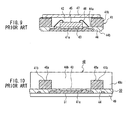
- FIG. 9 shows the solid-state imaging device disclosed in JP 2001-77277A, which is a conventional example of such a solid-state imaging device.
- numeral 41 denotes a housing, which is made of a base 41a and frame-shaped ribs 41b formed in one piece by resin molding, thus forming an internal space 42.
- a die pad 43 positioned at the center of the base 41a and leads 44 positioned below the ribs 41b are embedded in the housing 41.
- An imaging element chip 45 disposed at the center of the internal space 42 is fixed to the upper side of the die pad 43.
- the leads 44 include inner terminal portions 44a that are exposed to the internal space 42 at the upper side of the base 41a on the inner side of the ribs 41b and outer terminal portions 44b that are accessible from the bottom side of the base 41a below the ribs 41b.
- the inner terminal portions 44a and the bonding pads of the imaging element chip 45 are connected by bonding wires 46 made of metal.
- a transparent sealing glass plate 47 is fixed to the upper surface of the ribs 41b, thus forming a package for protection of the imaging element chip 45.
- This solid-state imaging device is mounted on a circuit board with the sealing glass plate 47 facing upward, as shown in FIG. 9, and the outer terminal portions 44b are used to connect it to the electrodes on the circuit board.
- a lens barrel incorporating an imaging optical system whose relative position to the photo-detecting region formed in the imaging element chip 45 is adjusted with a predetermined precision, is mounted on top of the sealing glass plate 47. During the imaging operation, object light that has passed through the imaging optical system incorporated in the lens barrel is focused on the photo-detecting region and photoelectrically converted.
- the upper surface of the ribs 41a has at least a certain width. Ensuring a sufficient width for the ribs 41b is an impediment to miniaturizing the area of the housing 41.
- a method for manufacturing a solid-state imaging device includes: resin-molding a housing including a base and rectangular frame-shaped ribs in one piece with a plurality of metal lead pieces, forming internal terminal portions and external terminal portions with the metal lead pieces; fixing an imaging element onto the base inside an internal space of the housing; connecting electrodes of the imaging element respectively to the inner terminal portions of the metal lead pieces; and fixing a transparent plate to an upper face of the ribs.
- a stepped portion is formed on the top face of the ribs, providing a lower step that is lowered along an internal periphery, the transparent plate has a size capable of being mounted onto an upper surface of the lower step within a region inward of an inner wall formed by the stepped portion of the ribs, and when fixing the transparent plate to the upper face of the ribs, an adhesive is provided on the upper face of the lower step, the transparent plate is placed on the adhesive to be fixed to the upper surface of the lower step while regulating its position with the inner wall of the stepped portion, and then the portion positioned outside the stepped portion of the ribs is removed.
- a plurality of the housings are molded together with a plurality of the metal lead pieces being arranged respectively, so that rib forming members are formed with the ribs forming adjacent housings combined into one, and a protruding portion is provided on the upper face of the rib forming members in the center in width direction so as to extend in a longitudinal direction, forming the stepped portion.
- FIGS. 1 to 4 show the structure of a solid-state imaging device made by this manufacturing method.
- FIG. 1 is a cross-sectional view
- FIG. 2 is a bottom view
- FIG. 3 is a lateral view of the solid-state imaging device.
- FIG 4 is a plan view showing the solid-state imaging device with a portion of its elements removed.
- Numeral 1 denotes a housing made of a thermosetting resin or a thermoplastic resin, such as epoxy resin, having ribs 3 arranged as a rectangular frame on a planar base 2 and fabricated by molding in one piece.
- An imaging element 5 is fixed by a fixing member 6 such as an adhesive onto the base 2 which faces an internal space 4 of the housing 1.
- a transparent plate 7 made of, for example, glass is fixed on the upper face of the ribs 3 by an adhesive 8, sealing the internal space 4 of the housing 1 and forming the package.
- the height of the ribs 3 is in a range of 0.1 to 1.0 mm for example, and the width of the ribs is set to 0.1 to 1.0 mm for example.
- a plurality of metal lead pieces 9 are embedded in the housing 1 at the time of molding.
- the metal lead pieces 9 are components for electrically leading from the internal space 4 of the housing 1 to the exterior and include an inner terminal portion 9a exposed on the surface of the internal space side of the base 2, an outer terminal portion 9b exposed on a rear surface of the base 2 at a position corresponding to the inner terminal portion 9a, and a lateral electrode portion 9c exposed on the lateral face of the housing 1.
- Electrode pads 5a of the imaging element 5 and the inner terminal portion 9a of the metal lead pieces 9 are connected by thin metal wires 10.
- the thickness of the entire package is set to no more than 2.0 mm, for example.
- FIG. 4 is a plan view of the solid-state imaging device in FIG. 1 without the transparent plate 7.
- the rear face corresponding to the position of the inner terminal portion 9a forms the outer terminal portion 9b.
- the metal lead pieces 9 in those portions are of substantially identical thickness as the base 2. Consequently, when resin forming it is possible to clamp the metal lead pieces 9 at the inner terminal portion 9a and the outer terminal portion 9b with the upper and lower molds. Thus, the surface of the inner terminal portions 9a is pressed down by the surface of the upper mold and is in close contact therewith, so that the generation of resin burr can be suppressed.
- the lateral electrode portions 9c located below the ribs 3 in the metal lead pieces 9 are formed to be thin by half-etching, and their bottom surface is covered by the resin.
- the external peripheral face of the housing 1, in other words, the external lateral face of the rib 3, forms a plane that is substantially perpendicular with respect to the face of the base 2. Further, the end face of the transparent plate 7 and the surface of the lateral electrode portion 9c are formed substantially flush with the external lateral faces of the housing 1.
- the internal peripheral face of the housing 1, in other words the internal lateral face of the rib 3, may be formed with a taper (not shown in drawings) which opens out from the surface of the base 2 in the direction of the transparent plate 7, for the purpose of allowing easy mold release after resin forming.
- the method for manufacturing a solid-state imaging device according to the present embodiment makes possible the efficient and highly accurate manufacturing of solid-state imaging devices having the above-described structure and performed by the steps explained below with reference to FIGS. 5 to 7.
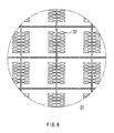
- a lead frame 21 is prepared. As shown in the plan view of FIG. 6, the lead frame 21 links a plurality of lead portions 22 in order to form the metal lead pieces 9 shown in FIG. 1.
- the thickness in the position corresponding to the internal terminal portion 9a of the lead portions 22 is set substantially identical to the thickness of the base 2.
- the lead portions 22 have a recessed portion 23 formed by half etching their lower surface, and by cutting this portion in a later process, this becomes the shape of the metal lead pieces 9 shown in FIG. 1.
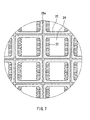
- FIG. 5B the lead frame 21 is embedded by insert molding with a resin so as to fabricate a molded article that includes a plurality of housings 26 made of a base 24 and a rib forming member 25.
- FIG. 7 shows the plan view after molding.
- the upper and lower faces of the lead portion 22 are embedded so as to be exposed from the upper and lower face of each base 24, and form the inner terminal portion 9a and the outer terminal portion 9b.
- the rib forming member 25 has a shape obtained by combining the ribs of adjacent housings 26 into one.
- a protruding portion 25a is formed on the central portion of the upper face of the rib forming members 25 such that it extends in the longitudinal direction of the rib forming members 25 (see FIG. 7). Consequently, a stepped portion 25c is formed by the side walls on both sides of the protruding portion 25a, and thereby, in the inner portion of each housing 26, the upper face of the rib forming members 25 forms a lower step 25b.
- the imaging element 5 is fixed by the adhesive 6 in the internal space which is enclosed by the rib forming member 25, and the pad electrodes 5a of the imaging element 5 are connected to the internal terminal portions 9a by the thin metal wires 10.
- an adhesive 28 is coated onto the upper face of the lower step 25b on both sides of the protruding portion 25a.
- the rib forming members 25, the lead portion 22 and the base 24 are cut with a dicing blade 29, and separated into pieces forming individual solid-state imaging devices as shown in FIG 5E.
- the cutting is performed in a direction perpendicular to the base 24, such that the width of the ribs 25 is halved, when viewed from above.
- the cutting is performed such that the region of the protruding portion 25a of the rib forming members 25 is eliminated.
- the housing 1 made of the base 2 and the ribs 3, and the metal lead pieces 9, are formed by the divided rib forming members 25, the lead portion 22 and the base 24. Furthermore, the lateral electrode portions 9c of the metal lead pieces 9 are exposed.
- the position of the transparent plates 7 can be regulated by the inner peripheral end face of the stepped portion 25c forming the protruding portion 25a.
- the width of the upper face of the rib forming members 25 is made small, positioning the transparent plate 7 is easy and reliable, and the width of the rib forming member 25 is no impediment to miniaturization of the housing.
- the shape of the protruding portion 25a for the purpose of regulating position is also no impediment with respect to the miniaturization of the housing.
- the width of the ribs 25 in a range that is sufficient for applying the adhesive for adhering the transparent plate 7.
- the ribs 25 are formed with the same width as the individually formed ribs and then cut in two pieces, then the width of the ribs 3 after the cutting can be made of half that in the conventional example.
- the cutting plane is perpendicular to the substrate portion 24.
- a taper for breaking the molded article from the mold after molding has to be provided on the outer lateral surface of the ribs. Consequently, the surface area of ribs that are fabricated in accordance with the present invention is reduced by the amount saved by not providing that outer taper portion.
- the rib forming member 25 and the lead portions 22 are cut together with the same dicing blade 29, the lateral surface of the package, which is formed by the end face of the transparent cover 7, the lateral surface of the casing 1, and the end surface of the metal lead strips 9, are substantially flush, and a favorable degree of flatness can be attained. Consequently, when mounting the device in the lens barrel accommodating the optical system, positioning of the optical system with respect to the photo-detecting portion of the imaging element 5 can be performed with high precision utilizing the lateral face of the package. That is to say, the device easily can be positioned with regard to the horizontal position by abutting the lateral surface of the package against the inner surface of the lens barrel. It should be noted that the positioning in the vertical direction can be performed by abutting the lower surface of the lens barrel against the circuit board surface.
- FIG. 8B a resin is filled into the cavity, and the base 24 and the rib forming member 25 are molded. After that, the dies are opened as shown in FIG. 8C, and a molded product of linked housings as shown in FIG. 5B is retrieved.
Landscapes
- Solid State Image Pick-Up Elements (AREA)
- Transforming Light Signals Into Electric Signals (AREA)
Applications Claiming Priority (2)
| Application Number | Priority Date | Filing Date | Title |
|---|---|---|---|
| JP2003293545 | 2003-08-14 | ||
| JP2003293545A JP3838571B2 (ja) | 2003-08-14 | 2003-08-14 | 固体撮像装置の製造方法 |
Publications (2)
| Publication Number | Publication Date |
|---|---|
| EP1507295A2 true EP1507295A2 (fr) | 2005-02-16 |
| EP1507295A3 EP1507295A3 (fr) | 2006-05-24 |
Family
ID=33562806
Family Applications (1)
| Application Number | Title | Priority Date | Filing Date |
|---|---|---|---|
| EP04018210A Withdrawn EP1507295A3 (fr) | 2003-08-14 | 2004-07-31 | Procédé de fabrication de dispositifs de prises de vues à l'état solide |
Country Status (6)
| Country | Link |
|---|---|
| US (1) | US7268016B2 (fr) |
| EP (1) | EP1507295A3 (fr) |
| JP (1) | JP3838571B2 (fr) |
| KR (1) | KR100644185B1 (fr) |
| CN (1) | CN1581502A (fr) |
| TW (1) | TW200507222A (fr) |
Cited By (1)
| Publication number | Priority date | Publication date | Assignee | Title |
|---|---|---|---|---|
| CN101647115B (zh) * | 2007-03-14 | 2012-04-25 | 松下电器产业株式会社 | 半导体装置及其制造方法、拾光模块 |
Families Citing this family (15)
| Publication number | Priority date | Publication date | Assignee | Title |
|---|---|---|---|---|
| US20070040231A1 (en) * | 2005-08-16 | 2007-02-22 | Harney Kieran P | Partially etched leadframe packages having different top and bottom topologies |
| KR20060004885A (ko) * | 2005-12-24 | 2006-01-16 | 최현규 | 반도체 패키지, 그 제조방법 및 이미지 센서용 반도체패키지 모듈 |
| CN100454505C (zh) * | 2006-01-25 | 2009-01-21 | 矽品精密工业股份有限公司 | 半导体装置及其制法 |
| US7990727B1 (en) * | 2006-04-03 | 2011-08-02 | Aprolase Development Co., Llc | Ball grid array stack |
| US8609978B2 (en) * | 2007-02-14 | 2013-12-17 | Flextronics Ap, Llc | Leadframe based photo voltaic electronic assembly |
| JP2008226378A (ja) * | 2007-03-14 | 2008-09-25 | Matsushita Electric Ind Co Ltd | 半導体デバイス、その製造方法および光ピックアップモジュール |
| JP2008227232A (ja) * | 2007-03-14 | 2008-09-25 | Matsushita Electric Ind Co Ltd | 半導体デバイスの製造方法、半導体デバイスおよび光ピックアップモジュール |
| JP2008227233A (ja) * | 2007-03-14 | 2008-09-25 | Matsushita Electric Ind Co Ltd | 半導体デバイスの製造方法、光ピックアップモジュール、および半導体デバイス |
| DE102007024159B3 (de) * | 2007-05-24 | 2008-11-06 | Semikron Elektronik Gmbh & Co. Kg | Leistungshalbleitermodul |
| KR100927423B1 (ko) * | 2008-05-15 | 2009-11-19 | 삼성전기주식회사 | 글라스 캡 몰딩 패키지 및 그 제조방법, 그리고 카메라모듈 |
| JP5633480B2 (ja) * | 2011-06-30 | 2014-12-03 | 豊田合成株式会社 | 発光装置の製造方法 |
| JP2015038920A (ja) * | 2013-08-19 | 2015-02-26 | ソニー株式会社 | 撮像装置および電子機器 |
| CN113580690B (zh) * | 2016-03-08 | 2023-12-08 | 株式会社可乐丽 | 覆金属层叠板 |
| WO2019156051A1 (fr) * | 2018-02-08 | 2019-08-15 | 株式会社村田製作所 | Module haute fréquence |
| JP7181050B2 (ja) * | 2018-10-18 | 2022-11-30 | 浜松ホトニクス株式会社 | 放射線撮像装置 |
Family Cites Families (6)
| Publication number | Priority date | Publication date | Assignee | Title |
|---|---|---|---|---|
| JP2001077277A (ja) | 1999-09-03 | 2001-03-23 | Sony Corp | 半導体パッケージおよび半導体パッケージ製造方法 |
| US6384472B1 (en) * | 2000-03-24 | 2002-05-07 | Siliconware Precision Industries Co., Ltd | Leadless image sensor package structure and method for making the same |
| JP2002134762A (ja) * | 2000-10-19 | 2002-05-10 | Shinko Electric Ind Co Ltd | 光学装置及びその製造方法 |
| TW473951B (en) * | 2001-01-17 | 2002-01-21 | Siliconware Precision Industries Co Ltd | Non-leaded quad flat image sensor package |
| JP2002373950A (ja) | 2001-06-15 | 2002-12-26 | Seiko Instruments Inc | 気密封止icパッケージの製造方法 |
| TW521410B (en) * | 2001-11-15 | 2003-02-21 | Siliconware Precision Industries Co Ltd | Semiconductor package article |
-
2003
- 2003-08-14 JP JP2003293545A patent/JP3838571B2/ja not_active Expired - Fee Related
-
2004
- 2004-07-27 TW TW093122375A patent/TW200507222A/zh unknown
- 2004-07-28 US US10/901,850 patent/US7268016B2/en not_active Expired - Fee Related
- 2004-07-31 EP EP04018210A patent/EP1507295A3/fr not_active Withdrawn
- 2004-08-05 CN CNA2004100562289A patent/CN1581502A/zh active Pending
- 2004-08-13 KR KR1020040063816A patent/KR100644185B1/ko not_active Expired - Fee Related
Cited By (1)
| Publication number | Priority date | Publication date | Assignee | Title |
|---|---|---|---|---|
| CN101647115B (zh) * | 2007-03-14 | 2012-04-25 | 松下电器产业株式会社 | 半导体装置及其制造方法、拾光模块 |
Also Published As
| Publication number | Publication date |
|---|---|
| JP3838571B2 (ja) | 2006-10-25 |
| EP1507295A3 (fr) | 2006-05-24 |
| TW200507222A (en) | 2005-02-16 |
| US20050037538A1 (en) | 2005-02-17 |
| JP2005064292A (ja) | 2005-03-10 |
| KR100644185B1 (ko) | 2006-11-10 |
| US7268016B2 (en) | 2007-09-11 |
| CN1581502A (zh) | 2005-02-16 |
| KR20050019056A (ko) | 2005-02-28 |
Similar Documents
| Publication | Publication Date | Title |
|---|---|---|
| US7691678B2 (en) | Solid-state imaging device and method for manufacturing the same | |
| US7294907B2 (en) | Solid-state imaging device and method for manufacturing the same | |
| CN100459136C (zh) | 固体摄像器件及其制造方法 | |
| KR100652375B1 (ko) | 와이어 본딩 패키지를 포함하는 이미지 센서 모듈 구조물및 그 제조방법 | |
| US7719585B2 (en) | Solid-state imaging device | |
| US7247509B2 (en) | Method for manufacturing solid-state imaging devices | |
| US7268016B2 (en) | Method for manufacturing solid-state imaging devices | |
| JP2006332685A (ja) | 固体撮像装置 |
Legal Events
| Date | Code | Title | Description |
|---|---|---|---|
| PUAI | Public reference made under article 153(3) epc to a published international application that has entered the european phase |
Free format text: ORIGINAL CODE: 0009012 |
|
| AK | Designated contracting states |
Kind code of ref document: A2 Designated state(s): AT BE BG CH CY CZ DE DK EE ES FI FR GB GR HU IE IT LI LU MC NL PL PT RO SE SI SK TR |
|
| AX | Request for extension of the european patent |
Extension state: AL HR LT LV MK |
|
| PUAL | Search report despatched |
Free format text: ORIGINAL CODE: 0009013 |
|
| AK | Designated contracting states |
Kind code of ref document: A3 Designated state(s): AT BE BG CH CY CZ DE DK EE ES FI FR GB GR HU IE IT LI LU MC NL PL PT RO SE SI SK TR |
|
| AX | Request for extension of the european patent |
Extension state: AL HR LT LV MK |
|
| RIC1 | Information provided on ipc code assigned before grant |
Ipc: H01L 31/0203 20060101ALI20060403BHEP Ipc: H01L 27/146 20060101AFI20060403BHEP |
|
| 17P | Request for examination filed |
Effective date: 20061123 |
|
| AKX | Designation fees paid |
Designated state(s): DE FR GB |
|
| RAP1 | Party data changed (applicant data changed or rights of an application transferred) |
Owner name: PANASONIC CORPORATION |
|
| STAA | Information on the status of an ep patent application or granted ep patent |
Free format text: STATUS: THE APPLICATION HAS BEEN WITHDRAWN |
|
| 18W | Application withdrawn |
Effective date: 20090917 |