EP1508824A1 - Fibre optique à bande interdite photonique - Google Patents
Fibre optique à bande interdite photonique Download PDFInfo
- Publication number
- EP1508824A1 EP1508824A1 EP04255046A EP04255046A EP1508824A1 EP 1508824 A1 EP1508824 A1 EP 1508824A1 EP 04255046 A EP04255046 A EP 04255046A EP 04255046 A EP04255046 A EP 04255046A EP 1508824 A1 EP1508824 A1 EP 1508824A1
- Authority
- EP
- European Patent Office
- Prior art keywords
- media
- plural
- optical fiber
- permittivity
- photonic
- Prior art date
- Legal status (The legal status is an assumption and is not a legal conclusion. Google has not performed a legal analysis and makes no representation as to the accuracy of the status listed.)
- Granted
Links
Images



Classifications
-
- G—PHYSICS
- G02—OPTICS
- G02B—OPTICAL ELEMENTS, SYSTEMS OR APPARATUS
- G02B6/00—Light guides; Structural details of arrangements comprising light guides and other optical elements, e.g. couplings
- G02B6/10—Light guides; Structural details of arrangements comprising light guides and other optical elements, e.g. couplings of the optical waveguide type
- G02B6/12—Light guides; Structural details of arrangements comprising light guides and other optical elements, e.g. couplings of the optical waveguide type of the integrated circuit kind
-
- G—PHYSICS
- G02—OPTICS
- G02B—OPTICAL ELEMENTS, SYSTEMS OR APPARATUS
- G02B6/00—Light guides; Structural details of arrangements comprising light guides and other optical elements, e.g. couplings
- G02B6/02—Optical fibres with cladding with or without a coating
- G02B6/02295—Microstructured optical fibre
- G02B6/02314—Plurality of longitudinal structures extending along optical fibre axis, e.g. holes
- G02B6/02319—Plurality of longitudinal structures extending along optical fibre axis, e.g. holes characterised by core or core-cladding interface features
- G02B6/02323—Core having lower refractive index than cladding, e.g. photonic band gap guiding
- G02B6/02328—Hollow or gas filled core
-
- G—PHYSICS
- G02—OPTICS
- G02B—OPTICAL ELEMENTS, SYSTEMS OR APPARATUS
- G02B6/00—Light guides; Structural details of arrangements comprising light guides and other optical elements, e.g. couplings
-
- G—PHYSICS
- G02—OPTICS
- G02B—OPTICAL ELEMENTS, SYSTEMS OR APPARATUS
- G02B6/00—Light guides; Structural details of arrangements comprising light guides and other optical elements, e.g. couplings
- G02B6/02—Optical fibres with cladding with or without a coating
- G02B6/02295—Microstructured optical fibre
- G02B6/02314—Plurality of longitudinal structures extending along optical fibre axis, e.g. holes
- G02B6/02342—Plurality of longitudinal structures extending along optical fibre axis, e.g. holes characterised by cladding features, i.e. light confining region
- G02B6/02347—Longitudinal structures arranged to form a regular periodic lattice, e.g. triangular, square, honeycomb unit cell repeated throughout cladding
- G02B6/02352—Complex periodic lattices or multiple interpenetrating periodic lattices, e.g. unit cell having more than two materials, partially internally coated holes, for multiple bandgaps
Definitions
- the present invention relates to photonic bandgap optical fibers, and more particularly, to photonic bandgap optical fibers capable of guiding light of multiple bands by use of a photonic crystal structure forming plural band-gaps.
- optical fibers consist of a core of glass or plastic material having a higher refractive index inside a clad of glass or plastic material having a lower refractive index. Light propagates along the inner core due to total internal reflection, by which information can be sent.
- the optical fibers are so light-weighted and thin that they do not take up much space, but provide a high transmission speed and a low error rate.
- optical fibers are widely used in data transmission fields requiring a high rate of data transmission and reception and high reliability.
- light propagates through a solid core so that the core material causes scattering, dispersion, or absorption loss, which limit their efficiency.
- photonic band-gap optical fibers which guide light by means of photonic band-gaps are of more interest even though the refractive index of the core is lower than that of the clad.
- a photonic crystal structure is used to form photonic band-gaps.
- the photonic crystal structure has dimensions on the order of a few hundred nm to a few thousand ⁇ m depending on the frequency band to be used, and has substances with different refractive indexes that are regularly arranged.
- the photonic crystal is used to form a complete band-gap that does not pass polarized light irrespective of its incident angle, and further is used to form an absolute band-gap that passes no light independent of polarization. Due to such characteristics, the photonic crystal can be used to fabricate optical devices such as split filters, optical waveguides, optical delay devices, and optical fibers.
- the photonic crystal has three kinds of structures such as one dimensional, two dimensional, and three dimensional structures, depending upon the number of periodic orientations.
- a variety of detailed structures have been proposed for all dimensions. For example, if an appropriate structure is selected for a two-dimensional photonic crystal, an absolute band-gap can be formed that prevents light having a wavelength about two times longer than a grid constant from propagating in any direction within the periodic structure.
- the characteristics of such a photonic crystal are determined by factors such as grid shape, grid constant, shape of an inserted pile, and the like. Further, if a round pile is filled, the characteristics of the photonic crystal are determined by its radius, permittivity of a background material, permittivity of the filled pile, and the like.
- FIG. 1 is a view showing a two-dimensional photonic crystal structure.
- FIG. 1 depicts a photonic crystal whose cross-section is two dimensional (having two dimensions in the x-y cross-section), and where second media 15 of a cylindrical shape of radius of R having a second permittivity are periodically arranged in the first medium 13 having a first permittivity.
- the relationships between wave vectors and frequencies for the photonic crystal structure of FIG. 1 can be obtained by solving the Maxwell equations.
- FIG. 2 is a view showing band-gaps for the photonic crystal structure of FIG. 1 having a grid constant p and a propagation vector ⁇ in a z-direction which is a light propagation direction.
- silica having a refractive index of 1.45 is used for the first medium 13 and the filling factor is 0.7.
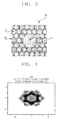
- FIG. 3 is a cross-sectioned view showing a conventional photonic band-gap optical fiber.
- a conventional photonic band-gap optical fiber 30 has a first medium 33 having a first permittivity and a second medium 35 of cylindrical shape arranged in the first medium 33 using the photonic crystal shown in FIG. 1.
- the photonic band-gap optical fiber 30 has a local hollow portion 37 formed in its center which breaks or rather interrupts the periodic arrangement of the second medium 35.
- the local hollow portion 37 formed in the center forms a defect mode so that light can propagate within the center of the fiber.
- FIG. 4 is a view showing a propagation mode of the conventional photonic band-gap optical fiber of FIG. 3.
- light is concentrated about the center of the photonic band-gap optical fiber.
- Light, excepting the center is blocked due to the band-gap, which can be seen by measuring the intensity of an electric field.
- the frequency band can be wider as compared with general optical fibers.
- the conventional photonic band-gap optical fiber is based on a photonic crystal structure having one band-gap for a specific propagation constant as a scale parameter is varied. Therefore, in a conventional photonic band-gap optical fiber, plural modes of light of different bands can not propagate at the same time. This is because its fundamental mode which allows light to propagate exists only in one band region.
- a photonic band-gap optical fiber comprising a photonic crystal having plural band-gaps, said photonic crystal comprising: a first medium having a first permittivity; plural second media having a second permittivity, and formed in a first periodic arrangement with respect to at least one or more directions on a plane formed of the first medium; and plural third media having a third permittivity, formed in a second periodic arrangement with respect to at least one or more directions on the plane formed of the first medium, and formed in a third periodic arrangement with respect to at least one or more directions together with the plural second media, wherein the photonic crystal has a hollow portion for propagating light passing through the plane formed of the first medium.
- the hollow portion is preferably formed to interrupt the first and second periodic arrangements of the plural second and third media. Further, the distance to the farthest point of the third media nearest from a center of the photonic crystal is preferably smaller than a distance to a nearest point of the second media nearest the center of the photonic crystal.
- the first, second and third permitivities are preferably different in value.
- the second permittivity is preferably larger in value than the first permittivity
- the third permittivity preferably has a value between the first permittivity and the second permittivity.
- the third media are preferably arranged within a unit cell formed of the plural second media or on boundaries of a unit cell formed of the plural second media. Further, the hollow portion can preferably be formed by omitting at least one or more of the plural second and third media at certain locations or by varying a size of at least one or more of the plural second and third media at certain locations.
- the present invention thus provides a photonic band-gap optical fiber through which plural modes of light of different bands can propagate by employing a photonic crystal having plural band-gaps for a specific propagation constant.
- FIG. 5 is a view showing a photonic crystal structure for use in a photonic band-gap optical fiber according to an embodiment of the present invention.
- the photonic crystal structure has a first medium 53 having a first permittivity, plural second media 55 having a second permittivity and formed in a first periodic arrangement with respect to at least one or more directions on a plane defined by the first medium 53, and plural third media 57 having a third permittivity and formed in a second periodic arrangement on a plane defined by the first medium 53.
- the third media 57 are arranged within unit cells formed of the second media 55 to form a third periodic arrangement with respect to at least one or more directions, together with the second media 55, to thereby form plural photonic band-gaps.
- FIG. 6 is a view showing band-gaps in the photonic crystal structure of FIG. 5.
- the x-axis represents the propagation constant value multiplied by a grid constant p
- the y-axis denotes frequency.
- the first medium 53 is silica having a refractive index of 1.45
- air is used for the second medium 55
- the radius of the second media 55 is 0.8 times R which is the radius before interpolation (filling factor is 0.7).
- Air is also used for the third media 57, and the radius of the third media 57 is 0 before interpolation, but 0.2 times the radius R after interpolation.
- the grid interval for the first periodicity of the second media 55 before interpolation is 2p
- the grid interval of the third periodicity of the second media 55 and third media 57 after interpolation is p.
- the photonic crystal structure used for the photonic band-gap optical fiber according to the present invention is described in detail in the Republic of Korea Patent Application No. 10-2002-0024761 entitled “Photonic Crystal Structure” filed by the Applicant.
- FIG. 7 is a cross-sectioned view showing a photonic bandgap optical fiber according to the present invention.
- the photonic band-gap optical fiber according to the present invention incorporates the photonic crystal shown in FIG. 5.
- the photonic band-gap optical fiber according to the present invention has a first medium 73 having a first permittivity, plural second media 75 formed in a first periodic arrangement in the first medium 73, and plural third media 77 formed in a second periodic arrangement, when viewed on an x-y plane.
- the photonic band-gap optical fiber has a hollow center 79 interrupting the periodic arrangements of the second media 75 and the third media 77.
- the second and third media 75 and 77 have second and third permittivities respectively, and the second permittivity is higher than the first permittivity, and the third permittivity has a value between the first permittivity and the second permittivity.
- the third media 77 are arranged so that the length from the center to the outermost edge is smaller than the distance from the second media 75 nearest the center. That is, the third media 77 each has a size that can be filled in unit cells formed of the plural second media 75, and are arranged so as not to overlap the second media 75. Further, the third media 77 are arranged within the unit cells formed of the plural second media 75, but can be used on the boundaries between the unit cells formed of the second dielectric substances.
- the hollow core 79 can be formed by omitting one or more of the plural periodically arranged second and third media 75 and 77.
- FIG. 7 shows a hollow core corresponding to seven second media 75.
- the hollow center 79 can be formed by omitting the second and third media 75 and 77 as above, and can also be formed by changing the size and shape of one or more of the periodic second and third media 75 and 77.
- FIG. 8 is a view showing propagation mode frequencies which vary depending upon propagation constants in the photonic band-gap optical fiber according to an embodiment of the present invention. That is, FIG. 8 shows band-gap variations and corresponding propagation modes depending on the magnitudes of the propagation vectors along the z-axis which represent the light propagation direction in the photonic band-gap optical fiber according to an embodiment of the present invention, and also shows a few fundamental modes and the second modes.
- FIG. 9 and FIG. 10 illustrate propagation modes appearing in the photonic band-gap optical fiber according to an embodiment of the present invention.
- FIG. 9 shows a mode calculated by use of the super cell method, that is, FIG. 9 shows a cross-sectional view as to the intensity of an electric field when the propagation constant is 4.3.
- a 14 x 14 super cell is used, and it is shown that the propagation frequencies exist in the band-gaps.
- FIG. 10 shows a cross section of a mode calculated by use of the super cell method in the case that the propagation constant is 7.0.
- a 12 x 12 super cell is used, and it shows that the propagation frequencies exist within the band-gaps.
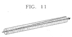
- FIG. 11 is a view showing propagation of two light beams having different bands in the photonic band-gap optical fiber according to an embodiment of the present invention.
- colors of light in red and blue represent the two different bands, and, as described above, light of different bands can propagate at the same time.
- the present invention can produce different propagation modes within plural band-gaps by use of a photonic crystal of the present invention forming plural band-gaps, through which light of plural, different bands can propagate at the same time.
Landscapes
- Physics & Mathematics (AREA)
- General Physics & Mathematics (AREA)
- Optics & Photonics (AREA)
- Engineering & Computer Science (AREA)
- Microelectronics & Electronic Packaging (AREA)
- Optical Fibers, Optical Fiber Cores, And Optical Fiber Bundles (AREA)
- Optical Integrated Circuits (AREA)
Applications Claiming Priority (2)
| Application Number | Priority Date | Filing Date | Title |
|---|---|---|---|
| KR2003058115 | 2003-08-22 | ||
| KR1020030058115A KR101018376B1 (ko) | 2003-08-22 | 2003-08-22 | 포토닉 밴드갭 광섬유 |
Publications (2)
| Publication Number | Publication Date |
|---|---|
| EP1508824A1 true EP1508824A1 (fr) | 2005-02-23 |
| EP1508824B1 EP1508824B1 (fr) | 2012-05-30 |
Family
ID=34056942
Family Applications (1)
| Application Number | Title | Priority Date | Filing Date |
|---|---|---|---|
| EP04255046A Expired - Lifetime EP1508824B1 (fr) | 2003-08-22 | 2004-08-20 | Fibre optique à bande interdite photonique |
Country Status (4)
| Country | Link |
|---|---|
| US (1) | US7016584B2 (fr) |
| EP (1) | EP1508824B1 (fr) |
| JP (1) | JP4272130B2 (fr) |
| KR (1) | KR101018376B1 (fr) |
Families Citing this family (3)
| Publication number | Priority date | Publication date | Assignee | Title |
|---|---|---|---|---|
| US8165441B2 (en) | 2008-03-26 | 2012-04-24 | Imra America, Inc. | Ultra small core fiber with dispersion tailoring |
| US8311373B1 (en) | 2009-07-22 | 2012-11-13 | The United States Of America As Represented By The Secretary Of The Navy | Capillary electrophoresis chemical sensor |
| KR101518599B1 (ko) | 2013-10-23 | 2015-05-07 | 주식회사 포스코 | 방진성이 우수한 고강도 고망간 강판 및 그 제조방법 |
Citations (2)
| Publication number | Priority date | Publication date | Assignee | Title |
|---|---|---|---|---|
| WO1999064904A1 (fr) * | 1998-06-09 | 1999-12-16 | Crystal Fibre A/S | Fibre a largeur de bande interdite photonique |
| WO2000006506A1 (fr) * | 1998-07-30 | 2000-02-10 | Corning Incorporated | Procede de fabrication de structures photoniques |
Family Cites Families (8)
| Publication number | Priority date | Publication date | Assignee | Title |
|---|---|---|---|---|
| US5600483A (en) * | 1994-05-10 | 1997-02-04 | Massachusetts Institute Of Technology | Three-dimensional periodic dielectric structures having photonic bandgaps |
| AU771646B2 (en) * | 1999-02-19 | 2004-04-01 | Crystal Fibre A/S | Improvements in or relating to photonic crystal fibres |
| WO2002012933A2 (fr) * | 2000-08-09 | 2002-02-14 | Massachusetts Institute Of Technology | Structure diélectrique périodique à intervalle interbande photonique tridimensionnel complet |
| US6625364B2 (en) * | 2001-01-25 | 2003-09-23 | Omniguide Communications | Low-loss photonic crystal waveguide having large core radius |
| US20020181911A1 (en) * | 2001-04-30 | 2002-12-05 | Wadsworth William John | Optical material and a method for its production |
| KR100390642B1 (ko) * | 2001-06-08 | 2003-07-07 | 학교법인 포항공과대학교 | 테라헤르츠파 전송을 위한 플라스틱 광결정 섬유 및 그제조 방법 |
| KR100441507B1 (ko) * | 2002-05-06 | 2004-07-23 | 삼성전자주식회사 | 포토닉 결정구조 |
| KR100518835B1 (ko) | 2002-12-02 | 2005-10-05 | 삼성전자주식회사 | 포토닉결정을 이용한 공진기 및 공진장치 |
-
2003
- 2003-08-22 KR KR1020030058115A patent/KR101018376B1/ko not_active Expired - Fee Related
-
2004
- 2004-08-20 US US10/921,858 patent/US7016584B2/en not_active Expired - Fee Related
- 2004-08-20 EP EP04255046A patent/EP1508824B1/fr not_active Expired - Lifetime
- 2004-08-23 JP JP2004242041A patent/JP4272130B2/ja not_active Expired - Fee Related
Patent Citations (3)
| Publication number | Priority date | Publication date | Assignee | Title |
|---|---|---|---|---|
| WO1999064904A1 (fr) * | 1998-06-09 | 1999-12-16 | Crystal Fibre A/S | Fibre a largeur de bande interdite photonique |
| US6539155B1 (en) * | 1998-06-09 | 2003-03-25 | Jes Broeng | Microstructured optical fibres |
| WO2000006506A1 (fr) * | 1998-07-30 | 2000-02-10 | Corning Incorporated | Procede de fabrication de structures photoniques |
Also Published As
| Publication number | Publication date |
|---|---|
| KR20050020846A (ko) | 2005-03-04 |
| KR101018376B1 (ko) | 2011-03-02 |
| EP1508824B1 (fr) | 2012-05-30 |
| US7016584B2 (en) | 2006-03-21 |
| JP2005070785A (ja) | 2005-03-17 |
| JP4272130B2 (ja) | 2009-06-03 |
| US20050041945A1 (en) | 2005-02-24 |
Similar Documents
| Publication | Publication Date | Title |
|---|---|---|
| US6573813B1 (en) | All-dielectric coaxial waveguide with annular sections | |
| US6788865B2 (en) | Polarization maintaining optical fiber with improved polarization maintaining property | |
| Chutinan et al. | Waveguides and waveguide bends in two-dimensional photonic crystal slabs | |
| EP1219984B1 (fr) | Guide d'ondes a cristal photonique | |
| EP1441244B1 (fr) | Fibre optique a maintien de polarisation et fibre optique a polarisation unique absolue | |
| US7116878B2 (en) | Optical waveguide structure | |
| JP2003513300A (ja) | リングフォトニック結晶ファイバ | |
| US9274276B2 (en) | Light confining devices using all-dielectric metamaterial cladding | |
| US20050146778A1 (en) | Two-dimensional photonic crystal optical multiplexer/demultiplexer | |
| JP2004527775A (ja) | 分散補償フォトニック結晶ファイバ | |
| US7133588B2 (en) | Device for bending an optical beam, in particular in an optical integrated circuit | |
| CN101546013A (zh) | 基于二维光子晶体多模干涉效应的波分复用器/解复用器 | |
| US7016584B2 (en) | Photonic bandgap optical fiber | |
| EP1460461B1 (fr) | Filtre d'insertion et d'extraction de canaux et dispositif de surveillance de canal à cristal photonique bidimensionnel | |
| US8768124B2 (en) | Direct coupling of optical slot waveguide to another optical waveguide | |
| Whittaker et al. | Photonic band structure of patterned waveguides with dielectric and metallic cladding | |
| VP et al. | Characteristics of photonic crystal fibers with different lattices: realization of constant air percentage by fixing air-filling fraction | |
| Shinya et al. | Single-mode transmission in commensurate width-varied line-defect SOI photonic crystal waveguides | |
| Pergande et al. | Coupling schemes for low-group velocity photonic crystal devices | |
| Thorhauge et al. | Properties of directional couplers using photonic crystal waveguides | |
| Mirlohi | Exact solutions of planar photonic crystal waveguides with infinite claddings | |
| JP2004101740A (ja) | フォトニック結晶導波路 | |
| JP2005274843A (ja) | 光制御素子 | |
| Shahamat et al. | Design and Simulation of a Waveguide Division De-multiplexer (DWDM) for Communication Application | |
| Fujisawa et al. | An Analysis of Air-Hole Type Photonic Crystal Waveguide Gratings Using Coupled-Mode Theory and Finite-Element Method |
Legal Events
| Date | Code | Title | Description |
|---|---|---|---|
| PUAI | Public reference made under article 153(3) epc to a published international application that has entered the european phase |
Free format text: ORIGINAL CODE: 0009012 |
|
| AK | Designated contracting states |
Kind code of ref document: A1 Designated state(s): AT BE BG CH CY CZ DE DK EE ES FI FR GB GR HU IE IT LI LU MC NL PL PT RO SE SI SK TR |
|
| AX | Request for extension of the european patent |
Extension state: AL HR LT LV MK |
|
| RIN1 | Information on inventor provided before grant (corrected) |
Inventor name: KIM, JI-DEOG Inventor name: LEE, SUK-HAN |
|
| 17P | Request for examination filed |
Effective date: 20050413 |
|
| 17Q | First examination report despatched |
Effective date: 20050511 |
|
| AKX | Designation fees paid |
Designated state(s): DE FR GB |
|
| 17Q | First examination report despatched |
Effective date: 20050511 |
|
| REG | Reference to a national code |
Ref country code: DE Ref legal event code: R079 Ref document number: 602004037963 Country of ref document: DE Free format text: PREVIOUS MAIN CLASS: G02B0006160000 Ipc: G02B0006032000 |
|
| GRAP | Despatch of communication of intention to grant a patent |
Free format text: ORIGINAL CODE: EPIDOSNIGR1 |
|
| RIC1 | Information provided on ipc code assigned before grant |
Ipc: G02B 6/036 20060101ALI20111202BHEP Ipc: G02B 6/02 20060101ALI20111202BHEP Ipc: G02B 6/032 20060101AFI20111202BHEP |
|
| GRAS | Grant fee paid |
Free format text: ORIGINAL CODE: EPIDOSNIGR3 |
|
| GRAA | (expected) grant |
Free format text: ORIGINAL CODE: 0009210 |
|
| AK | Designated contracting states |
Kind code of ref document: B1 Designated state(s): DE FR GB |
|
| REG | Reference to a national code |
Ref country code: GB Ref legal event code: FG4D |
|
| REG | Reference to a national code |
Ref country code: DE Ref legal event code: R096 Ref document number: 602004037963 Country of ref document: DE Effective date: 20120802 |
|
| RAP2 | Party data changed (patent owner data changed or rights of a patent transferred) |
Owner name: SAMSUNG ELECTRONICS CO., LTD. |
|
| PLBE | No opposition filed within time limit |
Free format text: ORIGINAL CODE: 0009261 |
|
| STAA | Information on the status of an ep patent application or granted ep patent |
Free format text: STATUS: NO OPPOSITION FILED WITHIN TIME LIMIT |
|
| 26N | No opposition filed |
Effective date: 20130301 |
|
| REG | Reference to a national code |
Ref country code: DE Ref legal event code: R097 Ref document number: 602004037963 Country of ref document: DE Effective date: 20130301 |
|
| PGFP | Annual fee paid to national office [announced via postgrant information from national office to epo] |
Ref country code: DE Payment date: 20130725 Year of fee payment: 10 |
|
| PGFP | Annual fee paid to national office [announced via postgrant information from national office to epo] |
Ref country code: FR Payment date: 20130725 Year of fee payment: 10 Ref country code: GB Payment date: 20130729 Year of fee payment: 10 |
|
| REG | Reference to a national code |
Ref country code: DE Ref legal event code: R119 Ref document number: 602004037963 Country of ref document: DE |
|
| GBPC | Gb: european patent ceased through non-payment of renewal fee |
Effective date: 20140820 |
|
| REG | Reference to a national code |
Ref country code: FR Ref legal event code: ST Effective date: 20150430 |
|
| REG | Reference to a national code |
Ref country code: DE Ref legal event code: R119 Ref document number: 602004037963 Country of ref document: DE Effective date: 20150303 |
|
| PG25 | Lapsed in a contracting state [announced via postgrant information from national office to epo] |
Ref country code: DE Free format text: LAPSE BECAUSE OF NON-PAYMENT OF DUE FEES Effective date: 20150303 Ref country code: GB Free format text: LAPSE BECAUSE OF NON-PAYMENT OF DUE FEES Effective date: 20140820 |
|
| PG25 | Lapsed in a contracting state [announced via postgrant information from national office to epo] |
Ref country code: FR Free format text: LAPSE BECAUSE OF NON-PAYMENT OF DUE FEES Effective date: 20140901 |