EP1508847B1 - Systéme de compensation de fréquence pour régulateurs à faible chute de tension (LDO) avec polarisation adaptative - Google Patents
Systéme de compensation de fréquence pour régulateurs à faible chute de tension (LDO) avec polarisation adaptative Download PDFInfo
- Publication number
- EP1508847B1 EP1508847B1 EP03368082A EP03368082A EP1508847B1 EP 1508847 B1 EP1508847 B1 EP 1508847B1 EP 03368082 A EP03368082 A EP 03368082A EP 03368082 A EP03368082 A EP 03368082A EP 1508847 B1 EP1508847 B1 EP 1508847B1
- Authority
- EP
- European Patent Office
- Prior art keywords
- impedance
- transistor
- gate
- circuit
- ldo
- Prior art date
- Legal status (The legal status is an assumption and is not a legal conclusion. Google has not performed a legal analysis and makes no representation as to the accuracy of the status listed.)
- Expired - Lifetime
Links
- 230000003044 adaptive effect Effects 0.000 title claims abstract description 27
- 238000000034 method Methods 0.000 claims abstract description 18
- 239000003990 capacitor Substances 0.000 claims description 28
- 230000000977 initiatory effect Effects 0.000 claims 2
- 230000006641 stabilisation Effects 0.000 abstract description 2
- 238000011105 stabilization Methods 0.000 abstract description 2
- 230000033228 biological regulation Effects 0.000 description 6
- 230000001052 transient effect Effects 0.000 description 6
- 238000004377 microelectronic Methods 0.000 description 2
- 230000001105 regulatory effect Effects 0.000 description 2
- 230000003542 behavioural effect Effects 0.000 description 1
- 230000007423 decrease Effects 0.000 description 1
- 239000000463 material Substances 0.000 description 1
- 230000010363 phase shift Effects 0.000 description 1
Images



Classifications
-
- G—PHYSICS
- G05—CONTROLLING; REGULATING
- G05F—SYSTEMS FOR REGULATING ELECTRIC OR MAGNETIC VARIABLES
- G05F1/00—Automatic systems in which deviations of an electric quantity from one or more predetermined values are detected at the output of the system and fed back to a device within the system to restore the detected quantity to its predetermined value or values, i.e. retroactive systems
- G05F1/10—Regulating voltage or current
- G05F1/46—Regulating voltage or current wherein the variable actually regulated by the final control device is DC
- G05F1/56—Regulating voltage or current wherein the variable actually regulated by the final control device is DC using semiconductor devices in series with the load as final control devices
- G05F1/575—Regulating voltage or current wherein the variable actually regulated by the final control device is DC using semiconductor devices in series with the load as final control devices characterised by the feedback circuit
Definitions
- This invention relates generally to voltage regulators, and more particularly to an enhancement of low dropout voltage regulators having an adaptive biased driving stage in order to improve stability through a very wide range of output current.
- LDO linear regulators are commonly used to provide power to low-voltage digital and analog circuits, where point-of-load and line regulation is important.
- Fig. 1 prior art shows a typical basic circuit of a LDO regulator 3 having an input voltage V i 1, an output voltage V o 2, an input current I i and an output current I o .
- Transient response is the behavioral of the regulator after a abrupt change of either the load current (load response) or the input voltage (line response). A minimum under and overshoot of the regulated voltage and a fast settling is desired.
- the transient response is defined by the frequency compensation of the regulation loop. Voltage regulators are difficult to compensate because of the fact that the load resistance and with this the output pole can vary over a wide range. For zero load the load resistance is infinite and the output pole is zero Hz. For maximum load the load resistance is at its minimum and the output pole is as its maximum, that might be a few KHz.
- U. S. Patent 6,246,221 to Xi . describes a high power supply ripple rejection (PSRR) internally compensated low drop-out (LDO) voltage regulator using an output PMOS pass device.
- PSRR power supply ripple rejection
- LDO low drop-out
- the voltage regulator uses a non-inversion variable gain amplifier stage to adjust its gain in response to a load current passing through the output PMOS device such that as the load current decreases, the gain increases, wherein a second pole associated with the voltage regulator is pushed above a unity gain frequency associated with the voltage regulator.
- Fig. 2 prior art shows a simplified circuit of an embodiment of a PMOS LDO according to said U.S. Patent 6,246,221 to Xi .
- Said regulator is a multiple-loop regulator.
- Said circuit comprises a gm-buffer amplifier 202 to push the gate pole of the PMOS pass device 201 to high frequencies.
- Transistor 203 serves for adaptive biasing the gm-buffer amplifier 202.
- 211 represents the equivalent series resistance (ESR) of the load capacitor 213.
- 212 represents the equivalent series inductance (ESL) of the load capacitor 213 . In case of low loads the out-pole formed by the load capacitor 213 and the load resistance 210 goes to low frequencies and thus it is possible to lower the gate-pole also.
- a LDO having an error amplifier as part of a current mirror output stage.
- a method and a circuit to achieve a low dropout voltage regulator having a constant high performance under all operating conditions, including the dropout region, has been disclosed in said patent application.
- a regulated cascade structure is placed at the input of a current mirror and in connection with a voltage regulator output stage.
- the positive input of the error amplifier is not biased with a reference voltage but connected to the regulator output. Therefore the cascade structure regulates the voltage of the entry node of the current mirror to be equal to the output voltage of the regulator under all operating conditions of the regulator.
- the transistors of the current mirror have always identical drain-source voltages. Therefore the regulator is kept in the optimal, balanced operating point, a constant high regulator loop gain is achieved and PSRR and load regulation performance is no more reduced under dropout operating conditions.
- Fig. 3 prior art shows a simplified circuit of an embodiment of a LDO according to the above mentioned non published European application 302 is the input transistor of a current mirror formed by PMOS pass device 301 and said input transistor 302 .
- Equivalent to Fig. 2 prior art 311 represents the equivalent series resistance (ESR) of the filter capacitor 313.
- 312 represents again the equivalent series inductance (ESL) of the filter capacitor 313.
- 310 represents the load resistance of said LDO again.
- the gate-pole of the PMOS pass device 301 moves in a constant ratio with the out-pole.
- Said gate-pole of the pass device is formed by the gate capacity C gate of transistor 301 and 1/gm of the input transistor 302, wherein gm represents the transconductance gain of transistor 302 .
- Said out-pole is formed by the load resistance 310 and the load capacitor 313.
- U. S. Patent Application Publication 2002/0130646 (to Zadeh et al. ) describes a linear voltage regulator, such as a low-dropout regulator, supplying power to one or more digital circuits within a computer system.
- the low-dropout regulator provides a substantially constant output voltage independent of loading conditions.
- the low-dropout regulator is biased at a relatively low operating current for steady-state operation to improve power efficiency of the low-dropout regulator.
- an adaptive biasing circuit senses the loading condition change and provides additional biasing current to momentarily increase the operating current of the low-dropout regulator to improve transient response.
- EP-A-0 779 568 discloses a method for reducing the transient response time of a voltage regulator when the load attached to it is entering or exiting a lower power consumption level by changing the bandwidth of the voltage regulator, based on a signal sent by a control device when it senses that the component is about to change power consumption level.
- US 6 603 292 discloses a low drop-out voltage regulator having an adaptive zero frequency circuit maintaining the stability of the LDO regulator and improving the transient response of the LDO regulator under a range of values for the output current, whereas the output current inversely varies with the load resistance coupled to the output of the LDO regulator.
- EP-A-0 862 102 discloses a load pole stabilized regulator.
- a principal object of the present invention is b improve the stability of low dropout voltage regulators (LDO) having an adaptive biased driving stage.
- LDO low dropout voltage regulators
- a further object of the present invention is to keep the current consumption of said LDOs at a minimum.
- a circuit to improve the stability of a low drop-out (LDO) voltage regulator comprises a means of an adaptive biased driving stage of said LDO, an impedance being connected on one side to said means of an adaptive biased driving stage and on the other side to the gate of a pass device of said LDO, a pass device of said LDO, wherein its gate is connected to said impedance and the source and drain are connected to V DD voltage and to the output voltage of said LDO, and a filter capacitor being connected to ground and to the output voltage of said LDO.
- a method to improve the stability of a low drop-out (LDO) voltage regulator comprises first providing a pass device for an adaptive biased driving stage.
- the steps of the method invented are to add a serial impedance to the gate capacitance of said pass device and to shunt partly said impedance in case of medium load currents as far as required.
- the preferred embodiments disclose circuits and a method for enhancements of low drop-out (LDO) voltage regulators having adaptive biased driving stages in order to improve the stability of the regulation loop of said LDOs.
- Said embodiments of the present invention can be used e.g. in multiple loop regulators as disclosed in U.S. 6,246,221 and described in the prior art section of this application or can be used e.g. with LDOs using current mirrors.
- the gate pole formed by the inner resistance of the driving stage and the gate capacitance of the PMOS pass device, is at least N times higher than the output pole formed by load resistance and the load capacitance.
- N has to be equal or higher than the open-loop gain of the LDO.
- the open-loop gain is 60 dB, i.e. 1000, then N has to be higher than 1000.
- This statement is only valid as long the inductances can be neglected.
- LDO circuits use capacitors having a capacitance in the order of magnitude of 1 - 3 ⁇ F. Said capacitors may have a serial inductance of about 1nH.
- the PCB routing, the chip package and the bonding wires of the package may also have 1 - 20 nH inductance. Therefore the resonance frequency of the out "tank" is in the order of magnitude of 500 KHz to 3 MHz.
- the LDO gets instable for high currents as explained below.
- Fig. 4 shows a preferred embodiment of the present invention. It shows a circuit of an LDO using an adaptive biased gm-buffer, similar to the circuit described in Fig. 2 prior art. In the circuit shown in Fig. 4 a gm-buffer 402 pushes the gate pole of the pass device 401 to high frequencies.
- Transistor 403 provides adaptive biasing of the gm-buffer 402 .
- Resistor 411 represents the equivalent series resistance (ESR) of the filter capacitor 413.
- Inductor 412 represents the equivalent series inductance (ESL) of the filter capacitor 413. In case of low loads the output-pole formed by the load 410 and the capacitance 413 goes to low frequencies and it is therefore possible to lower the gate pole.
- Said preferred embodiment shown in Fig. 4 is thus characterized that a serial resistor 420 is added to the gate capacitance.
- a resistor has been selected.
- Another kind of impedance, e.g. a transistor, besides a resistor could have been used as well.
- Fig. 5 shows another embodiment of the present invention: Said circuit shown in Fig. 5 is similar to the circuit shown in Fig. 4 .
- Fig. 5 shows again a circuit of an LDO using an adaptive biased gm-buffer, similar to the circuit described in Fig. 2 prior art.
- a gm-buffer 502 pushes the gate pole of the pass device 501 to high frequencies.
- Transistor 503 provides adaptive biasing of the gm-buffer 502.
- Resistor 511 represents the equivalent series resistance (ESR) of the filter capacitor 513.
- Inductor 512 represents the equivalent series inductance (ESL) of the filter capacitor 513 .
- Said preferred embodiment shown in Fig. 5 is thus characterized that a serial resistor 520 is added to the to the gate capacitance and, differentiating from the circuit shown in Fig. 4 .
- the adaptive biasing transistor 503 is connected to the gate of the pass device 501 and not, as shown in Fig. 4 , to the output of the adaptive biased gm-buffer. There is no difference in functionality between the circuit shown in Fig. 4 and the circuit shown in Fig. 5 .
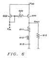
- Fig. 6 shows another embodiment of the present invention: Said circuit shown in Fig. 6 is similar to the circuit shown in Fig. 3 prior art . Fig. 6 shows also a circuit of an LDO using a current mirror.
- 602 is the input transistor of a current mirror formed by PMOS pass device 601 and said input transistor 602 .
- Resistor 611 represents the equivalent series resistance (ESR) of the filter capacitor 613 .
- Inductor 612 represents the equivalent series inductance (ESL) of the filter capacitor 613 .
- the gate pole which is formed by the gate capacity of the pass device 601 and by the reciprocal value of the transconductance 1/gm of said input transistor 602 of said current mirror, moves in a constant ratio with the output pole, which is formed by the capacity of the filter capacitor 613 and by the resistance of the load 610 .
- a serial resistor 620 is added to the gate capacitance of said pass device 601 .
- another kind of impedance e.g. a transistor, could be used as well.
- said resistance of said resistor 620 is not dominating, in case of high load said resistance keeps the gate pole close to the resonance frequency of the output "tank", formed by the capacitor 613 and the equivalent series inductance (ESL) of the filter capacitor 613 .
- said resonance frequency is defined by the equivalent series inductance (ESL) 612 and by the capacitance of the capacitor 613 .
- the resistance of the serial resistor 420 respective 520 or 620 is during low load conditions, i.e. low frequencies, small compared to the inner resistance of the gm-buffer 402 respective 502 or the inner resistance input of the current mirror shown in Fig. 6 .
- the gate pole could be too low.
- a possible solution of said problem could be to increase the ratio N of the gate pole to the output pole but this has the disadvantage of a higher current consumption.
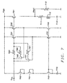
- Fig. 7 shows another embodiment of the present invention solving the problem of medium loads.
- V IN represents the input voltage of an adaptive biased driving stage, e.g. a gm-buffer or the gate voltage of an input transistor of a current mirror
- V OUT represents the output voltage of the LDO shown.
- Equivalent to Fig. 2-6 resistor 711 represents the equivalent series resistance (ESR) of the filter capacitor 713.
- 712 represents the equivalent series inductance (ESL) of the filter capacitor 713.
- 710 represents the load resistance of said LDO.
- ESR equivalent series resistance
- ESL equivalent series inductance
- Transistor 750 generates the gate voltage for the transistors 751 and 752 .
- Transistors 731 and 732 generate currents in a fixed ratio to the output current.
- I 731 is the current flowing through transistor 731
- I 770 is the current provided by the current source 770
- L 750 is the gate length of transistor 750
- W 750 is the gate width of transistor 750
- L 751 is the gate length of transistor 751
- W 751 is the gate width of transistor 751
- the resistor 720 is shunted in two steps.
- I 732 is the current flowing through transistor 732
- I 770 is the current provided by the current source 770
- L 750 is the gate length of transistor 750
- W 750 is the gate width of transistor 750
- L 752 is the gate length of transistor 752
- W 752 is the gate width of transistor 752
- the total serial gate resistance of the PMOS pass device 701 can be tuned according to the requirements.
- the serial resistor 720 can be shunted stepwise for different load currents having a medium load order of magnitude.
- the gate resistance of the PMOS pass device 701 in case of medium load currents the gate pole can be thus held on the optimum frequency.
- the ratio N can be reduced as far as possible.
- the current consumption of the driving stage can be kept to a minimum.
- the shunting of the serial gate resistor can be performed by one step only or by more than one step. Shunting in two steps has been shown in Fig. 7 and has been explained above. In case shunting in one step is desired then transistors 732, 752, 742 and the resistor 782 are not required. In case three steps of shunting are desired additional transistors can be deployed in parallel to transistors 732, 752 and 742 and a additional resistor can be deployed in the same way as resistors 781 and 782 . It is obvious that more than three steps of shunting can be introduced also by adding correspondent additional transistors and resistors.
- Fig. 8 shows the basic steps of a method to increase the stability of an LDO comprising a pass device.
- the first step 81 as described above, comprises to add a serial impedance to the gate capacitance of said pass device.
- the next step 82 comprises to shunt said impedance partly as far as required in case of medium load currents.
Landscapes
- Engineering & Computer Science (AREA)
- Physics & Mathematics (AREA)
- Electromagnetism (AREA)
- General Physics & Mathematics (AREA)
- Radar, Positioning & Navigation (AREA)
- Automation & Control Theory (AREA)
- Continuous-Control Power Sources That Use Transistors (AREA)
- Amplifiers (AREA)
- Optical Head (AREA)
- Power Conversion In General (AREA)
Claims (24)
- Un circuit destiné à améliorer la stabilité d'un régulateur à faible chute de tension (LDO) comportant :- un circuit de transfert (401, 501, 601, 701) doté d'une source et d'un drain connectés au potentiel VDD et au potentiel de sortie dudit régulateur LDO ;- un filtrage capacitif (413, 513, 613, 713) connecté à la terre et au potentiel de sortie dudit LDO ; et- des moyens d'un étage de commande de polarisation adaptatif (402, 403, 502, 503) dudit LDO pour emmener le pole de la grille du circuit de transfert vers les fréquences hautes ;caractérisé en ce qu'il comporte :- une impédance série (420, 520, 620, 720) connectée en permanence, d'un côté, à la sortie desdits moyens d'un étage de commande de polarisation adaptatif et, de l'autre côté, à la grille dudit circuit de transfert afin de conserver le pole de la grille du circuit de transfert proche de la fréquence de résonance définie par l'inductance série équivalent (ESL) et par la capacité du filtrage capacitif.
- Le circuit selon la revendication 1 dans lequel ladite impédance est une résistance.
- Le circuit selon la revendication 1 dans lequel ladite impédance résulte d'un transistor.
- Le circuit selon la revendication 1 dans lequel ladite impédance peut être réduite lors de conditions de charge spécifique au moyen d'une impédance parallèle additionnelle.
- Le circuit selon la revendication 4 dans lequel ladite condition de charge spécifique est une condition de charge moyenne.
- Le circuit selon la revendication 4 dans lequel ladite impédance parallèle est un transistor.
- Le circuit selon la revendication 4 dans lequel ladite impédance parallèle est un transistor avec une résistance en série.
- Le circuit selon la revendication 4 comportant des moyens pour réduire ladite impédance en au moins deux étapes en fonction de la valeur du courant de charge.
- Le circuit selon la revendication 8 comportant des moyens pour réduire ladite impédance, à chaque étape, au moyen d'une résistance additionnelle mise en parallèle sur la première résistance.
- Le circuit selon la revendication 9 dans lequel lesdites impédances parallèles additionnelles sont réalisées par des transistors disposés en parallèle.
- Le circuit selon la revendication 8 dans lequel lesdites impédance parallèles additionnelles sont réalisées par des transistors ayant une résistance en série, lesquels sont disposés en parallèle.
- Le circuit selon la revendication 4 comportant un circuit spécial pour la détection de conditions spécifiques de charge en vue de l'opération de réduction de l'impédance connectée à la grille du circuit de transfert en fonction de la valeur du courant de charge dudit LDO.
- Le circuit selon la revendication 12 dans lequel la condition de charge spécifique est une condition de charge moyenne.
- Le circuit selon la revendication 12, dans lequel le circuit spécial comporte une source de courant (770) connectée à la terre et à un premier transistor (750), qui est connecté via deux additionnels second et troisième transistors (761, 762), opérant comme des circuit de décalages de tension vers le potentiel VDD et de plus la grille dudit premier transistor (750) est connectée à ladite source de courant (770) et à la grille d'un quatrième transistor (751), qui est connecté à la terre et à un cinquième transistor (731), qui est connecté au potentiel VDD et à la grille d'un sixième transistor (741) réalisant une mise en parallèle sur l'impédance à réduire, et dans lequel la grille dudit cinquième transistor (731) est connectée à l'impédance devant être réduite.
- Le circuit selon la revendication 12, comportant des moyens de détection d'une condition de charge spécifique et pour engager une réduction de l'impédance de grille dudit circuit de transfert (701) en plus d'une étape, dans lequel ledit circuit spécial comporte une source de courant (770) connectée à la terre et à un premier transistor (750), qui est connecté via deux additionnels second et troisième transistors (761, 762), opérant comme des circuit de décalages de tension vers le potentiel VDD et de plus la grille dudit premier transistor (750) est connectée à ladite source de courant (770) et à la grille d'un quatrième transistor (751), qui est connecté à la terre et à un cinquième transistor (731), qui est connecté au potentiel VDD et à la grille d'un sixième transistor (741) réalisant une mise e parallèle sur l'impédance à réduire, et dans lequel la grille dudit cinquième transistor (731) est connectée à l'impédance devant être réduite, et comportant en outre des moyens pour introduire en parallèle audit quatrième (751) et cinquième transistor (731) deux additionnels septième et huitième transistors (752, 732) pour chacune des étapes de la réduction de l'impédance, lesdits transistors additionnels (752, 732) commandant la grille d'un neuvième transistor (742) qui est une mise en parallèle additionnelle sur l'impédance à réduire.
- Une méthode pour améliorer la stabilité d'un régulateur à faible chute de tension (LDO) comportant :- fournir un circuit de transfert (401, 501, 601, 701) doté d'une source et d'un drain connectés au potentiel VDD et au potentiel de sortie dudit régulateur LDO ;- fournir un filtrage capacitif (413, 513, 613, 713) connecté à la terre et au potentiel de sortie dudit LDO ; et- fournir des moyens d'un étage de commande de polarisation adaptatif (402, 403, 502, 503) dudit LDO pour emmener le pole de la grille du circuit de transfert vers les fréquences hautes ;caractérisé en ce qu'il comporte en outre:- ajouter une impédance série (420, 520, 620, 720) connectée en permanence, d'un côté, à la sortie desdits moyens d'un étage de commande de polarisation adaptatif et, de l'autre côté, à la grille dudit circuit de transfert afin de conserver le pole de la grille du circuit de transfert proche de la fréquence de résonance définie par l'inductance série équivalent (ESL) et par la capacité du filtrage capacitif.
- La méthode selon la revendication 16 dans laquelle l'étage de commande de polarisation adaptative est un tampon gm.
- La méthode selon la revendication 16 dans laquelle l'étage de commande de polarisation adaptative est un miroir de courant
- La méthode selon la revendication 16 dans laquelle ladite impédance série est un transistor.
- La méthode selon la revendication 1 dans laquelle ladite impédance série est une résistance.
- La méthode selon la revendication 16 dans laquelle ladite impédance série est partiellement court-circuitée en tant que de besoin lors de courant de charge de valeur moyenne.
- La méthode selon la revendication 21 dans laquelle ladite impédance série est mise en parallèle par sur un transistor.
- La méthode selon la revendication 21 dans laquelle ladite impédance série est mise en parallèle par sur un transistor ayant une résistance en série.
- La méthode selon la revendication 21 dans laquelle ladite impédance série est mise en parallèle en plus d'une étape.
Priority Applications (4)
| Application Number | Priority Date | Filing Date | Title |
|---|---|---|---|
| DE60318702T DE60318702D1 (de) | 2003-08-22 | 2003-08-22 | Frequenzkompensationsanordnung für Spannungsregler mit niedriger Abfallspannung (LDO) und mit anpassbarem Arbeitspunkt |
| EP03368082A EP1508847B1 (fr) | 2003-08-22 | 2003-08-22 | Systéme de compensation de fréquence pour régulateurs à faible chute de tension (LDO) avec polarisation adaptative |
| AT03368082T ATE384288T1 (de) | 2003-08-22 | 2003-08-22 | Frequenzkompensationsanordnung für spannungsregler mit niedriger abfallspannung (ldo) und mit anpassbarem arbeitspunkt |
| US10/706,837 US7030677B2 (en) | 2003-08-22 | 2003-11-12 | Frequency compensation scheme for low drop out voltage regulators using adaptive bias |
Applications Claiming Priority (1)
| Application Number | Priority Date | Filing Date | Title |
|---|---|---|---|
| EP03368082A EP1508847B1 (fr) | 2003-08-22 | 2003-08-22 | Systéme de compensation de fréquence pour régulateurs à faible chute de tension (LDO) avec polarisation adaptative |
Publications (2)
| Publication Number | Publication Date |
|---|---|
| EP1508847A1 EP1508847A1 (fr) | 2005-02-23 |
| EP1508847B1 true EP1508847B1 (fr) | 2008-01-16 |
Family
ID=34043014
Family Applications (1)
| Application Number | Title | Priority Date | Filing Date |
|---|---|---|---|
| EP03368082A Expired - Lifetime EP1508847B1 (fr) | 2003-08-22 | 2003-08-22 | Systéme de compensation de fréquence pour régulateurs à faible chute de tension (LDO) avec polarisation adaptative |
Country Status (4)
| Country | Link |
|---|---|
| US (1) | US7030677B2 (fr) |
| EP (1) | EP1508847B1 (fr) |
| AT (1) | ATE384288T1 (fr) |
| DE (1) | DE60318702D1 (fr) |
Families Citing this family (17)
| Publication number | Priority date | Publication date | Assignee | Title |
|---|---|---|---|---|
| US6975099B2 (en) * | 2004-02-27 | 2005-12-13 | Texas Instruments Incorporated | Efficient frequency compensation for linear voltage regulators |
| FR2872305B1 (fr) * | 2004-06-24 | 2006-09-22 | St Microelectronics Sa | Procede de controle du fonctionnement d'un regulateur a faible chute de tension et circuit integre correspondant |
| US7170269B1 (en) * | 2005-05-16 | 2007-01-30 | National Semiconductor Corporation | Low dropout regulator with control loop for avoiding hard saturation |
| US20070090815A1 (en) * | 2005-10-24 | 2007-04-26 | Faraday Technology Corp. | Integrated circuit with power gating function |
| FR2896051B1 (fr) | 2006-01-09 | 2008-04-18 | St Microelectronics Sa | Regulateur de tension serie a faible tension d'insertion |
| US7728569B1 (en) * | 2007-04-10 | 2010-06-01 | Altera Corporation | Voltage regulator circuitry with adaptive compensation |
| CN100480944C (zh) * | 2007-05-15 | 2009-04-22 | 北京中星微电子有限公司 | 一种压控电流源及带有压控电流源的低压差稳压电源 |
| US8278893B2 (en) * | 2008-07-16 | 2012-10-02 | Infineon Technologies Ag | System including an offset voltage adjusted to compensate for variations in a transistor |
| CN101866193B (zh) * | 2009-04-14 | 2012-05-09 | 上海立隆微电子有限公司 | 线性稳压电路与其控制芯片 |
| JP2011254338A (ja) * | 2010-06-03 | 2011-12-15 | Toshiba Corp | 半導体装置 |
| US9190907B2 (en) * | 2013-08-29 | 2015-11-17 | Intersil Americas LLC | System and method of equivalent series inductance cancellation |
| EP2857922A1 (fr) | 2013-10-07 | 2015-04-08 | Dialog Semiconductor GmbH | Circuits et procédé de commande de conditions de défaillance transitoire dans un régulateur à faible chute de tension |
| CN104950974B (zh) * | 2015-06-30 | 2017-05-31 | 华为技术有限公司 | 低压差线性稳压器与增加其稳定性的方法及锁相环 |
| US20170052552A1 (en) * | 2015-08-21 | 2017-02-23 | Qualcomm Incorporated | Single ldo for multiple voltage domains |
| US9921594B1 (en) * | 2017-04-13 | 2018-03-20 | Psemi Corporation | Low dropout regulator with thin pass device |
| IT201900006715A1 (it) * | 2019-05-10 | 2020-11-10 | St Microelectronics Srl | Circuito di compensazione in frequenza e dispositivo corrispondente |
| CN114740933B (zh) * | 2022-04-27 | 2022-12-02 | 电子科技大学 | 一种用于高压ldo的内部基准电源轨控制电路 |
Family Cites Families (9)
| Publication number | Priority date | Publication date | Assignee | Title |
|---|---|---|---|---|
| US4611154A (en) * | 1985-03-28 | 1986-09-09 | Gulf & Western Manufacturing Company | Method and apparatus for controlling the operation of a DC load |
| US4963814A (en) * | 1989-12-15 | 1990-10-16 | Boehringer Mannheim Corporation | Regulated bifurcated power supply |
| US5744944A (en) * | 1995-12-13 | 1998-04-28 | Sgs-Thomson Microelectronics, Inc. | Programmable bandwidth voltage regulator |
| KR100250628B1 (ko) * | 1996-10-30 | 2000-04-01 | 윤덕용 | 초고주파용 전계효과 트랜지스터 회로의 게이트단자 파형 왜곡 제어회로 |
| US5850139A (en) * | 1997-02-28 | 1998-12-15 | Stmicroelectronics, Inc. | Load pole stabilized voltage regulator circuit |
| US6246221B1 (en) * | 2000-09-20 | 2001-06-12 | Texas Instruments Incorporated | PMOS low drop-out voltage regulator using non-inverting variable gain stage |
| US6522111B2 (en) | 2001-01-26 | 2003-02-18 | Linfinity Microelectronics | Linear voltage regulator using adaptive biasing |
| US6603292B1 (en) * | 2001-04-11 | 2003-08-05 | National Semiconductor Corporation | LDO regulator having an adaptive zero frequency circuit |
| US6518737B1 (en) | 2001-09-28 | 2003-02-11 | Catalyst Semiconductor, Inc. | Low dropout voltage regulator with non-miller frequency compensation |
-
2003
- 2003-08-22 AT AT03368082T patent/ATE384288T1/de not_active IP Right Cessation
- 2003-08-22 EP EP03368082A patent/EP1508847B1/fr not_active Expired - Lifetime
- 2003-08-22 DE DE60318702T patent/DE60318702D1/de not_active Expired - Lifetime
- 2003-11-12 US US10/706,837 patent/US7030677B2/en not_active Expired - Lifetime
Also Published As
| Publication number | Publication date |
|---|---|
| US20050040799A1 (en) | 2005-02-24 |
| EP1508847A1 (fr) | 2005-02-23 |
| DE60318702D1 (de) | 2008-03-06 |
| US7030677B2 (en) | 2006-04-18 |
| ATE384288T1 (de) | 2008-02-15 |
Similar Documents
| Publication | Publication Date | Title |
|---|---|---|
| EP1508847B1 (fr) | Systéme de compensation de fréquence pour régulateurs à faible chute de tension (LDO) avec polarisation adaptative | |
| EP1378808B1 (fr) | Régulateur de tension à faible tension de déchet avec domaine de charge étendu et une boucle de contrôle rapide | |
| US6603292B1 (en) | LDO regulator having an adaptive zero frequency circuit | |
| US8278893B2 (en) | System including an offset voltage adjusted to compensate for variations in a transistor | |
| EP1569062B1 (fr) | Compensation de fréquence efficace pour régulateur de tension linéaire. | |
| US7545610B2 (en) | Constant-voltage power supply circuit with fold-back-type overcurrent protection circuit | |
| EP2031476B1 (fr) | Régulateur de tension et procédé de régulation de tension | |
| US20050184711A1 (en) | Low dropout voltage regulator | |
| US20070236292A1 (en) | Fast settling power amplifier regulator | |
| EP1336912A1 (fr) | Régulateur de tension à faible tension de déchêt | |
| US20040104711A1 (en) | Voltage regulator | |
| US9335779B2 (en) | Linear high speed tracking current sense system with positive and negative current | |
| CN100458634C (zh) | 用于微处理器电源或类似电源的有效电压配置装置 | |
| EP1580637B1 (fr) | Régulateur de tension continue à faible chute de tension | |
| US20090096436A1 (en) | Dc-dc converter | |
| EP1865397B1 (fr) | Régulateur de tension à faible chute | |
| US8253401B2 (en) | Voltage conversion apparatus | |
| US10775822B2 (en) | Circuit for voltage regulation and voltage regulating method | |
| US7049799B2 (en) | Voltage regulator and electronic device | |
| US20060091866A1 (en) | Power circuit | |
| US20040124925A1 (en) | Amplifier circuit and power supply provided therewith | |
| US11799427B2 (en) | Amplifier capacitive load compensation | |
| US11699947B2 (en) | DC-DC converters with loop control | |
| CN114513127A (zh) | 电压模式开关模式转换器中的补偿 | |
| KR20080017829A (ko) | 로우 드롭 아웃 레귤레이터 |
Legal Events
| Date | Code | Title | Description |
|---|---|---|---|
| PUAI | Public reference made under article 153(3) epc to a published international application that has entered the european phase |
Free format text: ORIGINAL CODE: 0009012 |
|
| AK | Designated contracting states |
Kind code of ref document: A1 Designated state(s): AT BE BG CH CY CZ DE DK EE ES FI FR GB GR HU IE IT LI LU MC NL PT RO SE SI SK TR |
|
| AX | Request for extension of the european patent |
Extension state: AL LT LV MK |
|
| 17P | Request for examination filed |
Effective date: 20050823 |
|
| AKX | Designation fees paid |
Designated state(s): AT BE BG CH CY CZ DE DK EE ES FI FR GB GR HU IE IT LI LU MC NL PT RO SE SI SK TR |
|
| 17Q | First examination report despatched |
Effective date: 20060202 |
|
| GRAP | Despatch of communication of intention to grant a patent |
Free format text: ORIGINAL CODE: EPIDOSNIGR1 |
|
| GRAS | Grant fee paid |
Free format text: ORIGINAL CODE: EPIDOSNIGR3 |
|
| GRAA | (expected) grant |
Free format text: ORIGINAL CODE: 0009210 |
|
| AK | Designated contracting states |
Kind code of ref document: B1 Designated state(s): AT BE BG CH CY CZ DE DK EE ES FI FR GB GR HU IE IT LI LU MC NL PT RO SE SI SK TR |
|
| REG | Reference to a national code |
Ref country code: GB Ref legal event code: FG4D |
|
| REG | Reference to a national code |
Ref country code: CH Ref legal event code: EP |
|
| REG | Reference to a national code |
Ref country code: IE Ref legal event code: FG4D |
|
| REF | Corresponds to: |
Ref document number: 60318702 Country of ref document: DE Date of ref document: 20080306 Kind code of ref document: P |
|
| PG25 | Lapsed in a contracting state [announced via postgrant information from national office to epo] |
Ref country code: NL Free format text: LAPSE BECAUSE OF FAILURE TO SUBMIT A TRANSLATION OF THE DESCRIPTION OR TO PAY THE FEE WITHIN THE PRESCRIBED TIME-LIMIT Effective date: 20080116 |
|
| NLV1 | Nl: lapsed or annulled due to failure to fulfill the requirements of art. 29p and 29m of the patents act | ||
| PG25 | Lapsed in a contracting state [announced via postgrant information from national office to epo] |
Ref country code: FI Free format text: LAPSE BECAUSE OF FAILURE TO SUBMIT A TRANSLATION OF THE DESCRIPTION OR TO PAY THE FEE WITHIN THE PRESCRIBED TIME-LIMIT Effective date: 20080116 Ref country code: ES Free format text: LAPSE BECAUSE OF FAILURE TO SUBMIT A TRANSLATION OF THE DESCRIPTION OR TO PAY THE FEE WITHIN THE PRESCRIBED TIME-LIMIT Effective date: 20080427 Ref country code: CH Free format text: LAPSE BECAUSE OF FAILURE TO SUBMIT A TRANSLATION OF THE DESCRIPTION OR TO PAY THE FEE WITHIN THE PRESCRIBED TIME-LIMIT Effective date: 20080116 Ref country code: LI Free format text: LAPSE BECAUSE OF FAILURE TO SUBMIT A TRANSLATION OF THE DESCRIPTION OR TO PAY THE FEE WITHIN THE PRESCRIBED TIME-LIMIT Effective date: 20080116 |
|
| REG | Reference to a national code |
Ref country code: CH Ref legal event code: PL |
|
| PG25 | Lapsed in a contracting state [announced via postgrant information from national office to epo] |
Ref country code: BG Free format text: LAPSE BECAUSE OF FAILURE TO SUBMIT A TRANSLATION OF THE DESCRIPTION OR TO PAY THE FEE WITHIN THE PRESCRIBED TIME-LIMIT Effective date: 20080416 Ref country code: AT Free format text: LAPSE BECAUSE OF FAILURE TO SUBMIT A TRANSLATION OF THE DESCRIPTION OR TO PAY THE FEE WITHIN THE PRESCRIBED TIME-LIMIT Effective date: 20080116 |
|
| ET | Fr: translation filed | ||
| PG25 | Lapsed in a contracting state [announced via postgrant information from national office to epo] |
Ref country code: BE Free format text: LAPSE BECAUSE OF FAILURE TO SUBMIT A TRANSLATION OF THE DESCRIPTION OR TO PAY THE FEE WITHIN THE PRESCRIBED TIME-LIMIT Effective date: 20080116 Ref country code: SI Free format text: LAPSE BECAUSE OF FAILURE TO SUBMIT A TRANSLATION OF THE DESCRIPTION OR TO PAY THE FEE WITHIN THE PRESCRIBED TIME-LIMIT Effective date: 20080116 Ref country code: PT Free format text: LAPSE BECAUSE OF FAILURE TO SUBMIT A TRANSLATION OF THE DESCRIPTION OR TO PAY THE FEE WITHIN THE PRESCRIBED TIME-LIMIT Effective date: 20080616 |
|
| PG25 | Lapsed in a contracting state [announced via postgrant information from national office to epo] |
Ref country code: SK Free format text: LAPSE BECAUSE OF FAILURE TO SUBMIT A TRANSLATION OF THE DESCRIPTION OR TO PAY THE FEE WITHIN THE PRESCRIBED TIME-LIMIT Effective date: 20080116 Ref country code: DK Free format text: LAPSE BECAUSE OF FAILURE TO SUBMIT A TRANSLATION OF THE DESCRIPTION OR TO PAY THE FEE WITHIN THE PRESCRIBED TIME-LIMIT Effective date: 20080116 Ref country code: SE Free format text: LAPSE BECAUSE OF FAILURE TO SUBMIT A TRANSLATION OF THE DESCRIPTION OR TO PAY THE FEE WITHIN THE PRESCRIBED TIME-LIMIT Effective date: 20080416 Ref country code: CZ Free format text: LAPSE BECAUSE OF FAILURE TO SUBMIT A TRANSLATION OF THE DESCRIPTION OR TO PAY THE FEE WITHIN THE PRESCRIBED TIME-LIMIT Effective date: 20080116 |
|
| PLBE | No opposition filed within time limit |
Free format text: ORIGINAL CODE: 0009261 |
|
| STAA | Information on the status of an ep patent application or granted ep patent |
Free format text: STATUS: NO OPPOSITION FILED WITHIN TIME LIMIT |
|
| PG25 | Lapsed in a contracting state [announced via postgrant information from national office to epo] |
Ref country code: RO Free format text: LAPSE BECAUSE OF FAILURE TO SUBMIT A TRANSLATION OF THE DESCRIPTION OR TO PAY THE FEE WITHIN THE PRESCRIBED TIME-LIMIT Effective date: 20080116 |
|
| 26N | No opposition filed |
Effective date: 20081017 |
|
| PG25 | Lapsed in a contracting state [announced via postgrant information from national office to epo] |
Ref country code: DE Free format text: LAPSE BECAUSE OF FAILURE TO SUBMIT A TRANSLATION OF THE DESCRIPTION OR TO PAY THE FEE WITHIN THE PRESCRIBED TIME-LIMIT Effective date: 20080417 |
|
| PG25 | Lapsed in a contracting state [announced via postgrant information from national office to epo] |
Ref country code: MC Free format text: LAPSE BECAUSE OF NON-PAYMENT OF DUE FEES Effective date: 20080831 |
|
| PG25 | Lapsed in a contracting state [announced via postgrant information from national office to epo] |
Ref country code: EE Free format text: LAPSE BECAUSE OF FAILURE TO SUBMIT A TRANSLATION OF THE DESCRIPTION OR TO PAY THE FEE WITHIN THE PRESCRIBED TIME-LIMIT Effective date: 20080116 |
|
| PG25 | Lapsed in a contracting state [announced via postgrant information from national office to epo] |
Ref country code: IE Free format text: LAPSE BECAUSE OF NON-PAYMENT OF DUE FEES Effective date: 20080822 Ref country code: CY Free format text: LAPSE BECAUSE OF FAILURE TO SUBMIT A TRANSLATION OF THE DESCRIPTION OR TO PAY THE FEE WITHIN THE PRESCRIBED TIME-LIMIT Effective date: 20080116 |
|
| PG25 | Lapsed in a contracting state [announced via postgrant information from national office to epo] |
Ref country code: HU Free format text: LAPSE BECAUSE OF FAILURE TO SUBMIT A TRANSLATION OF THE DESCRIPTION OR TO PAY THE FEE WITHIN THE PRESCRIBED TIME-LIMIT Effective date: 20080717 Ref country code: LU Free format text: LAPSE BECAUSE OF NON-PAYMENT OF DUE FEES Effective date: 20080822 |
|
| PG25 | Lapsed in a contracting state [announced via postgrant information from national office to epo] |
Ref country code: TR Free format text: LAPSE BECAUSE OF FAILURE TO SUBMIT A TRANSLATION OF THE DESCRIPTION OR TO PAY THE FEE WITHIN THE PRESCRIBED TIME-LIMIT Effective date: 20080116 |
|
| PG25 | Lapsed in a contracting state [announced via postgrant information from national office to epo] |
Ref country code: GR Free format text: LAPSE BECAUSE OF FAILURE TO SUBMIT A TRANSLATION OF THE DESCRIPTION OR TO PAY THE FEE WITHIN THE PRESCRIBED TIME-LIMIT Effective date: 20080417 |
|
| PGFP | Annual fee paid to national office [announced via postgrant information from national office to epo] |
Ref country code: IT Payment date: 20110824 Year of fee payment: 9 |
|
| PGFP | Annual fee paid to national office [announced via postgrant information from national office to epo] |
Ref country code: FR Payment date: 20120912 Year of fee payment: 10 |
|
| PG25 | Lapsed in a contracting state [announced via postgrant information from national office to epo] |
Ref country code: IT Free format text: LAPSE BECAUSE OF NON-PAYMENT OF DUE FEES Effective date: 20120822 |
|
| REG | Reference to a national code |
Ref country code: FR Ref legal event code: ST Effective date: 20140430 |
|
| PG25 | Lapsed in a contracting state [announced via postgrant information from national office to epo] |
Ref country code: FR Free format text: LAPSE BECAUSE OF NON-PAYMENT OF DUE FEES Effective date: 20130902 |
|
| PGFP | Annual fee paid to national office [announced via postgrant information from national office to epo] |
Ref country code: GB Payment date: 20190820 Year of fee payment: 17 |
|
| GBPC | Gb: european patent ceased through non-payment of renewal fee |
Effective date: 20200822 |
|
| PG25 | Lapsed in a contracting state [announced via postgrant information from national office to epo] |
Ref country code: GB Free format text: LAPSE BECAUSE OF NON-PAYMENT OF DUE FEES Effective date: 20200822 |