EP1509936B1 - Flüssigkeitshaltiges photovoltaisches element - Google Patents
Flüssigkeitshaltiges photovoltaisches element Download PDFInfo
- Publication number
- EP1509936B1 EP1509936B1 EP03733619A EP03733619A EP1509936B1 EP 1509936 B1 EP1509936 B1 EP 1509936B1 EP 03733619 A EP03733619 A EP 03733619A EP 03733619 A EP03733619 A EP 03733619A EP 1509936 B1 EP1509936 B1 EP 1509936B1
- Authority
- EP
- European Patent Office
- Prior art keywords
- electrode
- liquid
- counter
- conductors
- photovoltaic element
- Prior art date
- Legal status (The legal status is an assumption and is not a legal conclusion. Google has not performed a legal analysis and makes no representation as to the accuracy of the status listed.)
- Expired - Lifetime
Links
Images


Classifications
-
- H—ELECTRICITY
- H01—ELECTRIC ELEMENTS
- H01G—CAPACITORS; CAPACITORS, RECTIFIERS, DETECTORS, SWITCHING DEVICES, LIGHT-SENSITIVE OR TEMPERATURE-SENSITIVE DEVICES OF THE ELECTROLYTIC TYPE
- H01G9/00—Electrolytic capacitors, rectifiers, detectors, switching devices, light-sensitive or temperature-sensitive devices; Processes of their manufacture
- H01G9/20—Light-sensitive devices
- H01G9/2068—Panels or arrays of photoelectrochemical cells, e.g. photovoltaic modules based on photoelectrochemical cells
-
- H—ELECTRICITY
- H01—ELECTRIC ELEMENTS
- H01G—CAPACITORS; CAPACITORS, RECTIFIERS, DETECTORS, SWITCHING DEVICES, LIGHT-SENSITIVE OR TEMPERATURE-SENSITIVE DEVICES OF THE ELECTROLYTIC TYPE
- H01G9/00—Electrolytic capacitors, rectifiers, detectors, switching devices, light-sensitive or temperature-sensitive devices; Processes of their manufacture
- H01G9/20—Light-sensitive devices
- H01G9/2027—Light-sensitive devices comprising an oxide semiconductor electrode
- H01G9/2031—Light-sensitive devices comprising an oxide semiconductor electrode comprising titanium oxide, e.g. TiO2
-
- H—ELECTRICITY
- H10—SEMICONDUCTOR DEVICES; ELECTRIC SOLID-STATE DEVICES NOT OTHERWISE PROVIDED FOR
- H10K—ORGANIC ELECTRIC SOLID-STATE DEVICES
- H10K30/00—Organic devices sensitive to infrared radiation, light, electromagnetic radiation of shorter wavelength or corpuscular radiation
- H10K30/80—Constructional details
- H10K30/81—Electrodes
- H10K30/82—Transparent electrodes, e.g. indium tin oxide [ITO] electrodes
- H10K30/83—Transparent electrodes, e.g. indium tin oxide [ITO] electrodes comprising arrangements for extracting the current from the cell, e.g. metal finger grid systems to reduce the serial resistance of transparent electrodes
-
- Y—GENERAL TAGGING OF NEW TECHNOLOGICAL DEVELOPMENTS; GENERAL TAGGING OF CROSS-SECTIONAL TECHNOLOGIES SPANNING OVER SEVERAL SECTIONS OF THE IPC; TECHNICAL SUBJECTS COVERED BY FORMER USPC CROSS-REFERENCE ART COLLECTIONS [XRACs] AND DIGESTS
- Y02—TECHNOLOGIES OR APPLICATIONS FOR MITIGATION OR ADAPTATION AGAINST CLIMATE CHANGE
- Y02E—REDUCTION OF GREENHOUSE GAS [GHG] EMISSIONS, RELATED TO ENERGY GENERATION, TRANSMISSION OR DISTRIBUTION
- Y02E10/00—Energy generation through renewable energy sources
- Y02E10/50—Photovoltaic [PV] energy
- Y02E10/542—Dye sensitized solar cells
Definitions
- the invention relates to a liquid-containing photovoltaic element, comprising at least a plate-like work electrode and a plate-like counter-electrode adhered thereto by means of a vapour and liquid-tight peripheral edge, wherein a liquid is received in a space between the work electrode, the counter-electrode and the peripheral edge, a system of mutually connected electrical conductors being provided on the conductive layer of each of the substrates for the work electrode and the counter-electrode, which systems of conductors have a mirror-symmetrical form relative to each other, which conductors are provided with a layer of an electrically insulating material.
- Such a liquid-containing photovoltaic element is known from the international patent application WO-A-0048212.
- the known photovoltaic element comprises a work electrode which is formed by a layered structure of at least a first electrically conductive layer which is deposited on a first substrate, a layer of nanocrystalline metal oxide semiconductor material deposited on the first electrically conductive layer, a counter-electrode which is formed by a transparent second electrically conductive layer deposited on a transparent second substrate, and an electrolytic liquid contained between the layer of semiconductor material and the second electrically conductive layer.
- a glass plate for the first and second substrate.
- the contacts for drawing current from the element are arranged on edge zones of the element, wherein in all cases a first edge zone on a first substrate on which is formed a first contact does not extend opposite the second substrate, and vice versa, a second edge zone on a second substrate on which is formed a second contact does not extend opposite the first substrate.
- the substrate for the work electrode and the substrate for the counter-electrode in the known liquid-containing photovoltaic element are offset relative to each other so as to provide space for the electrical contacts. Offsetting of the substrates relative to each other results in a reduction of the available effective surface of the photovoltaic element, and thereby in a decrease, proportional to that reduction, in the maximum power of this element.
- liquid-containing photovoltaic element of the type stated in the preamble, wherein according to the invention there is provided in the layer of an electrically insulating material at least one recess for an electrical contact on a conductor, and wherein the electrically insulating material is an adhesive material, for instance a hot-melting plastic material.
- a photovoltaic element of which the conductors on the opposite electrodes are provided with a layer of adhesive material, can be manufactured in simple and cost-saving manner by placing the opposing adhesive layers into adhesive and sealing contact with each other.
- a thus manufactured element moreover provides the advantage that it is particularly stable and robust mechanically.
- a photovoltaic element according to the invention provides the option of arranging the contacts ( "tabs" ) for drawing current from the element on edge zones of the element, without it being required for this purpose that the substrate for the work electrode and the substrate for the counter-electrode are offset relative to each other.
- the mirror-symmetrical form of the conductor systems implies that the surfaces between the conductors, on respectively the work electrode (with the layer of semiconductor material) and the counter-electrode, also have a mirror-symmetrical form.
- the parts with a layer of semiconductor material and corresponding parts on the work electrode are also opposite, which enhances the efficiency of a photovoltaic element.
- the systems of conductors on the respective electrodes preferably have a congruent form so that during the manufacture of the work electrode and the counter-electrode use can be made of one type of substrate, which is provided with an electrically conductive layer on which the system of mutually connected electrical conductors is provided.
- the electrical conductors in each of the systems are mutually connected on at least a part of an edge zone of the respective substrates for the work electrode and the counter-electrode.
- This embodiment provides the option of forming a plurality of photovoltaic cells on two common, opposed substrates, wherein a contact for drawing current can be arranged in each case on the part of an edge zone where the conductors are mutually connected.
- the electrical conductors in each of the systems are mutually connected on an edge zone extending over the periphery of the respective substrates for the work electrode and the counter-electrode.
- one photovoltaic cell is formed on two opposite substrates, wherein a contact can be provided on each of the substrates at a position on the edge zone which can be freely chosen.
- the substrates for respectively the work electrode and the counter-electrode preferably have a mirror-symmetrical form relative to each other, more preferably the form of a rectangle or a regular polygon, most preferably a square form.
- a photovoltaic element with square substrates can be manufactured in particularly effective manner and thereby at relatively low cost, and using corresponding elements can be assembled into photovoltaic panels.
- the conductors extend in parallel manner from an edge zone over a distance which is smaller than half the width of the substrates.
- a photovoltaic element according to this latter embodiment provides particular advantages during manufacture thereof, since the space between the respective electrodes in an element with such conductors can be filled in rapid manner with electrolytic liquid. Filling takes place for instance by arranging a temporary filling opening in the centre of one of the substrates, placing the element on a rotatable disc, wherein the filling opening coincides with the rotation axis of the disc, and carrying the liquid into said space via the filling opening while simultaneously rotating the disc, in which space the liquid is driven in radial direction under the influence of the centrifugal force.
- Figures 1, 2, 3 show a liquid-containing photovoltaic element 1 which is assembled from square glass plates 2, 2', on which are successively arranged a TCO layer 3, 3' of the transparent conducting tin dioxide (SnO 2 :F) doped with fluorine and a pattern of silver (Ag) conductors 4, 4' which are covered by insulating layers 5, 5', fused to form a layer, of a hot-melting polymer foil, for instance a product commercially available from DuPont under the brand name Surlyn®.
- SnO 2 :F transparent conducting tin dioxide
- Ag silver
- a pattern 6 of dye-sensitized nanocrystalline titanium dioxide (TiO 2 ) is arranged between the insulated Ag conductors 4, on lower glass plate 2', 3', 4' a pattern 7 of a thin layer of platinum (Pt) is arranged between the insulated Ag conductors 4'.
- the upper substrate 2 with TCO layer 3, Ag pattern 4 and TiO 2 pattern 6 forms the work electrode
- Ag pattern 4' and Pt pattern 7' forms the counter-electrode.
- an electrolytic liquid 8 of for instance a lithium iodide-iodine solution (LiI-I).
- the Ag conductors 4, 4' are mutually connected by respective conductors which extend along the periphery and on which tabs 9, 9' are arranged for drawing current from element 1.
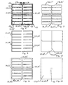
- Fig. 4 shows a pattern of Ag conductors 4, 4' on respectively the work electrode and the counter-electrode of the element 1 shown in fig. 1.
- Patterns 4, 4' are mirror-symmetrical and congruent, electrical conductors 4, 4' on the work electrode and the counter-electrode are mutually connected on an edge zone extending along the whole periphery of the respective substrate 2, 2', wherein conductors 4, 4' extend in parallel manner from an edge zone over a distance which is smaller than half the width of substrates 2, 2'.
- Fig. 5 shows a pattern of a sealing foil 5, 5', in which recesses 11, 11' are arranged for respective tabs 9, 9' in a manner such that a tab 9 arranged on a work electrode is left clear by foil 5 over the conductors 4 on that work electrode and is covered by foil 5' over the conductors 4' on the counter-electrode, and a tab 9' arranged on a counter-electrode is left clear by foil 5' over the conductors 4' on that counter-electrode and is covered by foil 5 over the conductors 4 on the work electrode.
- Fig. 6 shows the pattern of the TiO 2 layer 6 and the Pt layer 7', which is mirror-symmetrical and congruent therewith, on the substrates 2, 2' for respectively the work electrode and counter-electrode.
- Figure 7 shows the counter-electrode (substrate 2', dimensions 10 cm x 10 cm with Pt layer 7') during a phase in the production process prior to filling of the element with liquid, provided with a centrally placed filling opening 32 to be sealed after filling.
- Fig. 8 shows a liquid-containing photovoltaic element 10 assembled from four photovoltaic monocells 20 which are connected in series and which are made on quadrants of common square glass plates 2, 2' on which are successively arranged a TCO layer 13, 13' of SnO 2 :F and respective patterns of Ag conductors 14, 14', which are covered by insulating layers 15, 15' of a hot-melting polymer foil which are fused into respective layers.
- On upper glass plate 12, 13, 14 respective patterns 16 of dye-sensitized nanocrystalline TiO 2 are arranged between the insulated Ag conductors 14, on lower glass plate 12', 13', 14' respective patterns 17 of a thin layer of Pt are arranged between the insulated Ag conductors 14'.
- the respective TCO layers 13, Ag patterns 14 and TiO 2 patterns 16 on upper substrate 12 form the respective work electrodes
- the respective TCO layers 13', Ag patterns 14' and Pt patterns 17' on lower substrate 12' form the respective counter-electrodes.
- An electrolytic liquid is received in the spaces between the respective work electrodes and counter-electrodes.
- Ag conductors 14, 14' are mutually connected by respective conductors which extend along a part of the periphery and on which are arranged connections (not shown) between the individual monocells 20 for connecting in series thereof and tabs 9, 9' for drawing current from element 10.
- Fig. 9 shows patterns of Ag conductors 14, 14' on respectively the work electrodes and the counter-electrodes of monocells 20 of the element 10 shown in fig. 8.
- the patterns 14, 14' are separate for each monocell and mirror-symmetrical for element 10, the electrical conductors on the work electrodes and the counter-electrodes are mutually connected on an edge zone extending along a part of the periphery of the respective substrates, wherein the conductors extend in parallel manner from an edge zone over a distance which is smaller than half the width of the substrates.
- Fig. 10 shows a pattern of a sealing foil 15, 15' in which are arranged recesses 21, 21' for respective series connections (not shown) and respective tabs 19, 19' in a manner such that a tab 19 arranged on a work electrode is left clear by the foil 15 over conductors 14 on that work electrode, and is covered by the foil 15' over conductors 14' on the counter-electrode, and a tab 19' arranged on a counter-electrode is left clear by the foil 15' over conductors 14' on that counter-electrode, and is covered by foil 15 over conductors 14 on the work electrode.
- Fig. 11 shows the pattern of the respective TiO 2 layers 16 and, mirror-symmetrical and congruent therewith, the Pt layers 17' on the substrates for respectively the work electrodes and counter-electrodes.
- Fig. 12 shows substrate 12, 12' for the respective work electrodes and the counter-electrodes, provided with a TCO layer 13, 13' in which electrical insulation grooves 22, 22' are arranged between monocells 20 using a laser, and
- Fig. 13 shows the counter-electrodes (substrate 12', dimensions 30 cm x 30 cm with Pt layer 17') during a phase in the production process prior to filling of the element with liquid, provided with four centrally placed filling openings 42 to be sealed after filling.
Landscapes
- Engineering & Computer Science (AREA)
- Power Engineering (AREA)
- Microelectronics & Electronic Packaging (AREA)
- Chemical & Material Sciences (AREA)
- Chemical Kinetics & Catalysis (AREA)
- Electrochemistry (AREA)
- Photovoltaic Devices (AREA)
- Hybrid Cells (AREA)
- Sealing Battery Cases Or Jackets (AREA)
- Primary Cells (AREA)
Claims (10)
- Flüssigkeitshaltiges photovoltaisches Element (1; 10, 20), das eine plattenförmige Arbeitselektrode und eine mit Hilfe von einem dampf- und flüssigkeitsfesten Umfangsrand daran geheftete, plattenförmige Gegenelektrode umfasst, wobei die Arbeitselektrode und die Gegenelektrode beide auf einem mit einer elektrisch leitenden Schicht (3, 3'; 13, 13') versehenen, flachen Substrat (2, 2'; 12, 12') angebracht sind und wobei eine Flüssigkeit (8) in einem Raum zwischen der Arbeitselektrode, der Gegenelektrode und dem Umfangsrand aufgenommen ist, wobei auf der leitenden Schicht (3, 3'; 13, 13') von jedem der Substrate (2, 2'; 12, 12') für die Arbeitselektrode und die Gegenelektrode ein System von miteinander verbundenen elektrischen Leitern (4, 4'; 14, 14') verschafft ist, und diese Systeme von Leitern (4, 4'; 14, 14') haben in Bezug aufeinander eine spiegelsymmetrische Form, und diese Leiter (4, 4'; 14, 14') sind mit einer Schicht (5, 5'; 15, 15') von einem elektrisch isolierenden Material versehen, dadurch gekennzeichnet, dass in besagter isolierender Schicht (5, 5'; 15, 15') zumindest eine Aussparung (11, 11'; 21, 21') für einen elektrischen Kontakt (9, 9'; 19, 19') auf einem Leiter (4, 4'; 14, 14') verschafft ist, und dass das elektrisch isolierende Material ein Klebstoffmaterial (5, 5'; 15, 15') ist.
- Flüssigkeitshaltiges photovoltaisches Element (1; 10, 20) nach Anspruch 1, dadurch gekennzeichnet, dass das Klebstoffmaterial ein Heißschmelz-Kunststoffmaterial (5, 5'; 15, 15') ist.
- Flüssigkeitshaltiges photovoltaisches Element (1; 10, 20) nach einem der Ansprüche 1-2, dadurch gekennzeichnet, dass die Systeme von Leitern (4, 4'; 14, 14') auf den jeweiligen Elektroden eine kongruente Form haben.
- Flüssigkeitshaltiges photovoltaisches Element (1; 10, 20) nach einem der Ansprüche 1-3, dadurch gekennzeichnet, dass die elektrischen Leiter (4, 4'; 14, 14') in jedem der Systeme auf zumindest einem Teil einer Randzone der jeweiligen Substrate (2, 2'; 12, 12') für die Arbeitselektrode und die Gegenelektrode miteinander verbunden sind.
- Flüssigkeitshaltiges photovoltaisches Element (1) nach Anspruch 4, dadurch gekennzeichnet, dass die elektrischen Leiter (4, 4') in jedem der Systeme an einer sich über den Umfang der jeweiligen Substrate (2, 2') für die Arbeitselektrode und die Gegenelektrode erstreckenden Randzone miteinander verbunden sind.
- Flüssigkeitshaltiges photovoltaisches Element (1; 10, 20) nach einem der Ansprüche 1-5, dadurch gekennzeichnet, dass die Substrate (2, 2'; 12, 12') für jeweils die Arbeitselektrode und die Gegenelektrode in Bezug aufeinander eine spiegelsymmetrische Form haben.
- Flüssigkeitshaltiges photovoltaisches Element (1; 10, 20) nach Anspruch 6, dadurch gekennzeichnet, dass die Substrate (2, 2'; 12, 12') die Form eines regelmäßigen Polygons haben.
- Flüssigkeitshaltiges photovoltaisches Element (1; 10, 20) nach Anspruch 7, dadurch gekennzeichnet, dass die Substrate (2, 2'; 12, 12') eine quadratische Form haben.
- Flüssigkeitshaltiges photovoltaisches Element nach Anspruch 6, dadurch gekennzeichnet, dass die Substrate eine rechteckige Form haben.
- Flüssigkeitshaltiges photovoltaisches Element (1; 10, 20) nach einem der Ansprüche 8-9, dadurch gekennzeichnet, dass Leiter (4, 4'; 14, 14') sich von einer Randzone der jeweiligen Substrate (2, 2'; 12, 12') über einen Abstand, der kleiner als die halbe Breite besagter Substrate (2, 2'; 12, 12') ist, parallel erstrecken.
Applications Claiming Priority (3)
| Application Number | Priority Date | Filing Date | Title |
|---|---|---|---|
| NL1020744 | 2002-06-04 | ||
| NL1020744A NL1020744C2 (nl) | 2002-06-04 | 2002-06-04 | Vloeistofhoudend fotovoltaïsch element. |
| PCT/NL2003/000376 WO2003102986A1 (en) | 2002-06-04 | 2003-05-21 | Liquid-containing photovoltaic element |
Publications (2)
| Publication Number | Publication Date |
|---|---|
| EP1509936A1 EP1509936A1 (de) | 2005-03-02 |
| EP1509936B1 true EP1509936B1 (de) | 2006-01-18 |
Family
ID=29707802
Family Applications (1)
| Application Number | Title | Priority Date | Filing Date |
|---|---|---|---|
| EP03733619A Expired - Lifetime EP1509936B1 (de) | 2002-06-04 | 2003-05-21 | Flüssigkeitshaltiges photovoltaisches element |
Country Status (9)
| Country | Link |
|---|---|
| US (1) | US7253354B2 (de) |
| EP (1) | EP1509936B1 (de) |
| JP (1) | JP4594083B2 (de) |
| AT (1) | ATE316290T1 (de) |
| AU (1) | AU2003238712B2 (de) |
| DE (1) | DE60303301T2 (de) |
| ES (1) | ES2253681T3 (de) |
| NL (1) | NL1020744C2 (de) |
| WO (1) | WO2003102986A1 (de) |
Families Citing this family (36)
| Publication number | Priority date | Publication date | Assignee | Title |
|---|---|---|---|---|
| US8138413B2 (en) | 2006-04-13 | 2012-03-20 | Daniel Luch | Collector grid and interconnect structures for photovoltaic arrays and modules |
| US8664030B2 (en) | 1999-03-30 | 2014-03-04 | Daniel Luch | Collector grid and interconnect structures for photovoltaic arrays and modules |
| US7507903B2 (en) | 1999-03-30 | 2009-03-24 | Daniel Luch | Substrate and collector grid structures for integrated series connected photovoltaic arrays and process of manufacture of such arrays |
| US8222513B2 (en) | 2006-04-13 | 2012-07-17 | Daniel Luch | Collector grid, electrode structures and interconnect structures for photovoltaic arrays and methods of manufacture |
| US20090111206A1 (en) | 1999-03-30 | 2009-04-30 | Daniel Luch | Collector grid, electrode structures and interrconnect structures for photovoltaic arrays and methods of manufacture |
| US8198696B2 (en) | 2000-02-04 | 2012-06-12 | Daniel Luch | Substrate structures for integrated series connected photovoltaic arrays and process of manufacture of such arrays |
| US7022910B2 (en) * | 2002-03-29 | 2006-04-04 | Konarka Technologies, Inc. | Photovoltaic cells utilizing mesh electrodes |
| JP4161688B2 (ja) * | 2002-11-18 | 2008-10-08 | アイシン精機株式会社 | 湿式太陽電池 |
| IL153895A (en) * | 2003-01-12 | 2013-01-31 | Orion Solar Systems Ltd | Solar cell device |
| WO2008139479A2 (en) * | 2007-05-15 | 2008-11-20 | 3Gsolar Ltd. | Photovoltaic cell |
| JP2004327167A (ja) * | 2003-04-23 | 2004-11-18 | Sony Corp | 電解液の注入方法、湿式光電変換素子の製造方法および湿式装置の製造方法 |
| US7838868B2 (en) * | 2005-01-20 | 2010-11-23 | Nanosolar, Inc. | Optoelectronic architecture having compound conducting substrate |
| US7732229B2 (en) * | 2004-09-18 | 2010-06-08 | Nanosolar, Inc. | Formation of solar cells with conductive barrier layers and foil substrates |
| US7276724B2 (en) | 2005-01-20 | 2007-10-02 | Nanosolar, Inc. | Series interconnected optoelectronic device module assembly |
| US8927315B1 (en) | 2005-01-20 | 2015-01-06 | Aeris Capital Sustainable Ip Ltd. | High-throughput assembly of series interconnected solar cells |
| US9236512B2 (en) | 2006-04-13 | 2016-01-12 | Daniel Luch | Collector grid and interconnect structures for photovoltaic arrays and modules |
| US8822810B2 (en) | 2006-04-13 | 2014-09-02 | Daniel Luch | Collector grid and interconnect structures for photovoltaic arrays and modules |
| US8729385B2 (en) | 2006-04-13 | 2014-05-20 | Daniel Luch | Collector grid and interconnect structures for photovoltaic arrays and modules |
| US9865758B2 (en) | 2006-04-13 | 2018-01-09 | Daniel Luch | Collector grid and interconnect structures for photovoltaic arrays and modules |
| US9006563B2 (en) | 2006-04-13 | 2015-04-14 | Solannex, Inc. | Collector grid and interconnect structures for photovoltaic arrays and modules |
| US8884155B2 (en) | 2006-04-13 | 2014-11-11 | Daniel Luch | Collector grid and interconnect structures for photovoltaic arrays and modules |
| JP5649954B2 (ja) | 2007-04-02 | 2015-01-07 | メルク パテント ゲーエムベーハー | 光起電力セルとして構成される物品 |
| JP4488034B2 (ja) | 2007-06-29 | 2010-06-23 | 株式会社日立製作所 | 色素増感太陽電池 |
| MX2010005814A (es) * | 2007-11-27 | 2010-10-28 | 3Gsolar Ltd | Celdas colorantes de gran área y métodos de producción de las mismas. |
| US20090223511A1 (en) * | 2008-03-04 | 2009-09-10 | Cox Edwin B | Unglazed photovoltaic and thermal apparatus and method |
| TWI415271B (zh) * | 2009-02-09 | 2013-11-11 | Ind Tech Res Inst | 染料敏化太陽能電池 |
| US8247243B2 (en) * | 2009-05-22 | 2012-08-21 | Nanosolar, Inc. | Solar cell interconnection |
| KR101030013B1 (ko) * | 2009-08-26 | 2011-04-20 | 삼성에스디아이 주식회사 | 염료감응 태양전지 |
| FR2954856B1 (fr) * | 2009-12-30 | 2012-06-15 | Saint Gobain | Cellule photovoltaique organique et module comprenant une telle cellule |
| JP4935910B2 (ja) * | 2010-01-07 | 2012-05-23 | 大日本印刷株式会社 | 有機薄膜太陽電池 |
| CN101872686B (zh) * | 2010-06-22 | 2011-12-21 | 彩虹集团公司 | 一种染料敏化太阳能电池模块的制备方法 |
| CN104126271B (zh) * | 2011-01-10 | 2016-11-16 | 日芯光伏公司 | 太阳能发电装置 |
| KR101219245B1 (ko) * | 2011-04-21 | 2013-01-21 | 삼성에스디아이 주식회사 | 광전 변환 소자 및 이의 제조 방법 |
| US9000288B2 (en) * | 2011-07-22 | 2015-04-07 | Space Systems/Loral, Llc | Current collector bar and grid pattern for a photovoltaic solar cell |
| KR101241015B1 (ko) * | 2011-09-01 | 2013-03-11 | 현대자동차주식회사 | 집전극을 갖는 염료감응 태양전지 |
| US9627565B2 (en) | 2013-11-27 | 2017-04-18 | Space Systems/Loral, Llc | Integral corner bypass diode interconnecting configuration for multiple solar cells |
Family Cites Families (10)
| Publication number | Priority date | Publication date | Assignee | Title |
|---|---|---|---|---|
| JPS5788770A (en) * | 1980-11-21 | 1982-06-02 | Hitachi Ltd | Photo semiconductor device |
| JPS62142372A (ja) * | 1985-12-17 | 1987-06-25 | Semiconductor Energy Lab Co Ltd | 光電変換装置の作製方法 |
| JPH03269520A (ja) * | 1990-03-20 | 1991-12-02 | Ube Ind Ltd | 液晶表示パネルの製造法 |
| WO1996029715A1 (de) * | 1995-03-23 | 1996-09-26 | Ecole Polytechnique Federale De Lausanne (Epfl) | Verfahren zum herstellen eines langzeitstabilen moduls von photoelektrochemischen zellen |
| DE19726643C1 (de) | 1997-06-18 | 1998-07-23 | Francotyp Postalia Gmbh | Vorrichtung zur Reinigung eines Tintendruckkopfes |
| JP2002536805A (ja) * | 1999-02-08 | 2002-10-29 | クルス グラス プラス スピーゲル アクチエンゲゼルシヤフト | 光電池及びその製造方法 |
| JP3966638B2 (ja) * | 1999-03-19 | 2007-08-29 | 株式会社東芝 | 多色色素増感透明半導体電極部材とその製造方法、多色色素増感型太陽電池、及び表示素子 |
| JP4414036B2 (ja) * | 1999-12-27 | 2010-02-10 | シャープ株式会社 | 色素増感型太陽電池の作製方法 |
| US7202412B2 (en) * | 2002-01-18 | 2007-04-10 | Sharp Kabushiki Kaisha | Photovoltaic cell including porous semiconductor layer, method of manufacturing the same and solar cell |
| JP2004362793A (ja) * | 2003-06-02 | 2004-12-24 | Enplas Corp | 色素増感型太陽電池ユニット、色素増感型太陽電池用基板、及び色素増感型太陽電池ユニットの封止構造 |
-
2002
- 2002-06-04 NL NL1020744A patent/NL1020744C2/nl not_active IP Right Cessation
-
2003
- 2003-05-21 US US10/515,889 patent/US7253354B2/en not_active Expired - Fee Related
- 2003-05-21 EP EP03733619A patent/EP1509936B1/de not_active Expired - Lifetime
- 2003-05-21 WO PCT/NL2003/000376 patent/WO2003102986A1/en not_active Ceased
- 2003-05-21 AU AU2003238712A patent/AU2003238712B2/en not_active Ceased
- 2003-05-21 DE DE60303301T patent/DE60303301T2/de not_active Expired - Lifetime
- 2003-05-21 JP JP2004509978A patent/JP4594083B2/ja not_active Expired - Fee Related
- 2003-05-21 ES ES03733619T patent/ES2253681T3/es not_active Expired - Lifetime
- 2003-05-21 AT AT03733619T patent/ATE316290T1/de not_active IP Right Cessation
Also Published As
| Publication number | Publication date |
|---|---|
| JP4594083B2 (ja) | 2010-12-08 |
| US20060118165A1 (en) | 2006-06-08 |
| NL1020744C2 (nl) | 2003-12-08 |
| US7253354B2 (en) | 2007-08-07 |
| JP2005528750A (ja) | 2005-09-22 |
| WO2003102986A1 (en) | 2003-12-11 |
| DE60303301D1 (de) | 2006-04-06 |
| AU2003238712B2 (en) | 2009-01-08 |
| AU2003238712A1 (en) | 2003-12-19 |
| ES2253681T3 (es) | 2006-06-01 |
| EP1509936A1 (de) | 2005-03-02 |
| ATE316290T1 (de) | 2006-02-15 |
| DE60303301T2 (de) | 2006-10-26 |
Similar Documents
| Publication | Publication Date | Title |
|---|---|---|
| EP1509936B1 (de) | Flüssigkeitshaltiges photovoltaisches element | |
| EP1183698B1 (de) | Verfahren zum einbringen von zwischenverbindungen in regenerativen photovoltaischen photoelektrochemischen vielzellanordungen | |
| KR101131834B1 (ko) | 광전기화학 광전지 패널 및 그의 제조 방법 | |
| EP2022067B1 (de) | Versiegeltes monolithisches photo-elektrochemisches system und verfahren zur herstellung versiegelter monolithischer photo-elektrochemischer systeme | |
| JP2008130547A (ja) | 垂直積層型の色素感応太陽電池モジュール及びその製造方法 | |
| JP2009245750A (ja) | 色素増感太陽電池およびその製造方法 | |
| JP2009032614A (ja) | 色素増感型太陽電池の製造方法及び色素増感型太陽電池 | |
| US20150357123A1 (en) | Series/parallel mixed module structure of dye-sensitized solar cell and method of manufacturing the same | |
| KR100656357B1 (ko) | 금속 그리드를 포함하는 투명 전도성 기판 및 이를 구비한염료감응 태양전지 | |
| KR101217146B1 (ko) | 다수의 전극선을 포함한 염료 감응형 태양전지 | |
| KR100993847B1 (ko) | 염료감응 태양전지 모듈 및 그 제조방법 | |
| KR20050087903A (ko) | 교번 극성의 단위 셀의 배열구조를 갖는 염료감응형태양전지 | |
| JP4376707B2 (ja) | 透明太陽電池モジュール及びその製造方法 | |
| EP2359406B1 (de) | Photovoltaische elemente | |
| KR20130006088A (ko) | 염료감응 태양전지 단위 모듈을 이용한 타일 | |
| JP5685708B2 (ja) | 色素増感太陽電池の製造方法 | |
| JP2013201078A (ja) | 電気モジュール及び電気モジュールの製造方法 | |
| US20140007923A1 (en) | DSSC Photovoltaic Device Comprising Photoelectrochemical Cells and Provided with Bypass means and UV Filter | |
| KR101400637B1 (ko) | 태양전지를 이용한 블라인드 | |
| KR101206040B1 (ko) | 외부전극의 극성을 용이하게 변경할 수 있는 구조의 염료감응 태양전지 서브모듈 | |
| TWI535046B (zh) | 太陽能電池模組及其連接方法 | |
| KR101034217B1 (ko) | 염료감응 태양전지 제조방법 및 이에 의하여 제조된 염료감응 태양전지 | |
| WO2002035565A1 (en) | Sensors and array and method to manufacture thereof |
Legal Events
| Date | Code | Title | Description |
|---|---|---|---|
| PUAI | Public reference made under article 153(3) epc to a published international application that has entered the european phase |
Free format text: ORIGINAL CODE: 0009012 |
|
| 17P | Request for examination filed |
Effective date: 20041101 |
|
| AK | Designated contracting states |
Kind code of ref document: A1 Designated state(s): AT BE BG CH CY CZ DE DK EE ES FI FR GB GR HU IE IT LI LU MC NL PT RO SE SI SK TR |
|
| AX | Request for extension of the european patent |
Extension state: AL LT LV MK |
|
| 17Q | First examination report despatched |
Effective date: 20050411 |
|
| GRAP | Despatch of communication of intention to grant a patent |
Free format text: ORIGINAL CODE: EPIDOSNIGR1 |
|
| DAX | Request for extension of the european patent (deleted) | ||
| GRAS | Grant fee paid |
Free format text: ORIGINAL CODE: EPIDOSNIGR3 |
|
| GRAA | (expected) grant |
Free format text: ORIGINAL CODE: 0009210 |
|
| AK | Designated contracting states |
Kind code of ref document: B1 Designated state(s): AT BE BG CH CY CZ DE DK EE ES FI FR GB GR HU IE IT LI LU MC NL PT RO SE SI SK TR |
|
| PG25 | Lapsed in a contracting state [announced via postgrant information from national office to epo] |
Ref country code: SI Free format text: LAPSE BECAUSE OF FAILURE TO SUBMIT A TRANSLATION OF THE DESCRIPTION OR TO PAY THE FEE WITHIN THE PRESCRIBED TIME-LIMIT Effective date: 20060118 Ref country code: SK Free format text: LAPSE BECAUSE OF FAILURE TO SUBMIT A TRANSLATION OF THE DESCRIPTION OR TO PAY THE FEE WITHIN THE PRESCRIBED TIME-LIMIT Effective date: 20060118 Ref country code: AT Free format text: LAPSE BECAUSE OF FAILURE TO SUBMIT A TRANSLATION OF THE DESCRIPTION OR TO PAY THE FEE WITHIN THE PRESCRIBED TIME-LIMIT Effective date: 20060118 Ref country code: RO Free format text: LAPSE BECAUSE OF FAILURE TO SUBMIT A TRANSLATION OF THE DESCRIPTION OR TO PAY THE FEE WITHIN THE PRESCRIBED TIME-LIMIT Effective date: 20060118 Ref country code: FI Free format text: LAPSE BECAUSE OF FAILURE TO SUBMIT A TRANSLATION OF THE DESCRIPTION OR TO PAY THE FEE WITHIN THE PRESCRIBED TIME-LIMIT Effective date: 20060118 |
|
| REG | Reference to a national code |
Ref country code: GB Ref legal event code: FG4D |
|
| REG | Reference to a national code |
Ref country code: CH Ref legal event code: EP |
|
| REG | Reference to a national code |
Ref country code: IE Ref legal event code: FG4D |
|
| REF | Corresponds to: |
Ref document number: 60303301 Country of ref document: DE Date of ref document: 20060406 Kind code of ref document: P |
|
| PG25 | Lapsed in a contracting state [announced via postgrant information from national office to epo] |
Ref country code: DK Free format text: LAPSE BECAUSE OF FAILURE TO SUBMIT A TRANSLATION OF THE DESCRIPTION OR TO PAY THE FEE WITHIN THE PRESCRIBED TIME-LIMIT Effective date: 20060418 Ref country code: SE Free format text: LAPSE BECAUSE OF FAILURE TO SUBMIT A TRANSLATION OF THE DESCRIPTION OR TO PAY THE FEE WITHIN THE PRESCRIBED TIME-LIMIT Effective date: 20060418 Ref country code: BG Free format text: LAPSE BECAUSE OF FAILURE TO SUBMIT A TRANSLATION OF THE DESCRIPTION OR TO PAY THE FEE WITHIN THE PRESCRIBED TIME-LIMIT Effective date: 20060418 |
|
| REG | Reference to a national code |
Ref country code: CH Ref legal event code: NV Representative=s name: FELBER & PARTNER AG PATENTANWAELTE |
|
| PG25 | Lapsed in a contracting state [announced via postgrant information from national office to epo] |
Ref country code: IE Free format text: LAPSE BECAUSE OF NON-PAYMENT OF DUE FEES Effective date: 20060522 |
|
| PG25 | Lapsed in a contracting state [announced via postgrant information from national office to epo] |
Ref country code: MC Free format text: LAPSE BECAUSE OF NON-PAYMENT OF DUE FEES Effective date: 20060531 |
|
| REG | Reference to a national code |
Ref country code: ES Ref legal event code: FG2A Ref document number: 2253681 Country of ref document: ES Kind code of ref document: T3 |
|
| PG25 | Lapsed in a contracting state [announced via postgrant information from national office to epo] |
Ref country code: PT Free format text: LAPSE BECAUSE OF FAILURE TO SUBMIT A TRANSLATION OF THE DESCRIPTION OR TO PAY THE FEE WITHIN THE PRESCRIBED TIME-LIMIT Effective date: 20060619 |
|
| ET | Fr: translation filed | ||
| PLBE | No opposition filed within time limit |
Free format text: ORIGINAL CODE: 0009261 |
|
| STAA | Information on the status of an ep patent application or granted ep patent |
Free format text: STATUS: NO OPPOSITION FILED WITHIN TIME LIMIT |
|
| 26N | No opposition filed |
Effective date: 20061019 |
|
| PG25 | Lapsed in a contracting state [announced via postgrant information from national office to epo] |
Ref country code: CZ Free format text: LAPSE BECAUSE OF FAILURE TO SUBMIT A TRANSLATION OF THE DESCRIPTION OR TO PAY THE FEE WITHIN THE PRESCRIBED TIME-LIMIT Effective date: 20060118 Ref country code: GR Free format text: LAPSE BECAUSE OF FAILURE TO SUBMIT A TRANSLATION OF THE DESCRIPTION OR TO PAY THE FEE WITHIN THE PRESCRIBED TIME-LIMIT Effective date: 20060419 |
|
| PG25 | Lapsed in a contracting state [announced via postgrant information from national office to epo] |
Ref country code: EE Free format text: LAPSE BECAUSE OF FAILURE TO SUBMIT A TRANSLATION OF THE DESCRIPTION OR TO PAY THE FEE WITHIN THE PRESCRIBED TIME-LIMIT Effective date: 20060118 |
|
| PG25 | Lapsed in a contracting state [announced via postgrant information from national office to epo] |
Ref country code: LU Free format text: LAPSE BECAUSE OF NON-PAYMENT OF DUE FEES Effective date: 20060521 Ref country code: HU Free format text: LAPSE BECAUSE OF FAILURE TO SUBMIT A TRANSLATION OF THE DESCRIPTION OR TO PAY THE FEE WITHIN THE PRESCRIBED TIME-LIMIT Effective date: 20060719 Ref country code: TR Free format text: LAPSE BECAUSE OF FAILURE TO SUBMIT A TRANSLATION OF THE DESCRIPTION OR TO PAY THE FEE WITHIN THE PRESCRIBED TIME-LIMIT Effective date: 20060118 |
|
| PG25 | Lapsed in a contracting state [announced via postgrant information from national office to epo] |
Ref country code: CY Free format text: LAPSE BECAUSE OF FAILURE TO SUBMIT A TRANSLATION OF THE DESCRIPTION OR TO PAY THE FEE WITHIN THE PRESCRIBED TIME-LIMIT Effective date: 20060118 |
|
| PGFP | Annual fee paid to national office [announced via postgrant information from national office to epo] |
Ref country code: FR Payment date: 20110616 Year of fee payment: 9 Ref country code: ES Payment date: 20110630 Year of fee payment: 9 Ref country code: CH Payment date: 20110506 Year of fee payment: 9 |
|
| PGFP | Annual fee paid to national office [announced via postgrant information from national office to epo] |
Ref country code: NL Payment date: 20110524 Year of fee payment: 9 Ref country code: GB Payment date: 20110510 Year of fee payment: 9 |
|
| PGFP | Annual fee paid to national office [announced via postgrant information from national office to epo] |
Ref country code: BE Payment date: 20110601 Year of fee payment: 9 Ref country code: IT Payment date: 20110517 Year of fee payment: 9 Ref country code: DE Payment date: 20110527 Year of fee payment: 9 |
|
| BERE | Be: lapsed |
Owner name: *STICHTING ENERGIEONDERZOEK CENTRUM NEDERLAND Effective date: 20120531 |
|
| REG | Reference to a national code |
Ref country code: NL Ref legal event code: V1 Effective date: 20121201 |
|
| REG | Reference to a national code |
Ref country code: CH Ref legal event code: PL |
|
| GBPC | Gb: european patent ceased through non-payment of renewal fee |
Effective date: 20120521 |
|
| PG25 | Lapsed in a contracting state [announced via postgrant information from national office to epo] |
Ref country code: LI Free format text: LAPSE BECAUSE OF NON-PAYMENT OF DUE FEES Effective date: 20120531 Ref country code: CH Free format text: LAPSE BECAUSE OF NON-PAYMENT OF DUE FEES Effective date: 20120531 |
|
| PG25 | Lapsed in a contracting state [announced via postgrant information from national office to epo] |
Ref country code: IT Free format text: LAPSE BECAUSE OF NON-PAYMENT OF DUE FEES Effective date: 20120521 Ref country code: BE Free format text: LAPSE BECAUSE OF NON-PAYMENT OF DUE FEES Effective date: 20120531 |
|
| REG | Reference to a national code |
Ref country code: FR Ref legal event code: ST Effective date: 20130131 |
|
| REG | Reference to a national code |
Ref country code: DE Ref legal event code: R119 Ref document number: 60303301 Country of ref document: DE Effective date: 20121201 |
|
| PG25 | Lapsed in a contracting state [announced via postgrant information from national office to epo] |
Ref country code: NL Free format text: LAPSE BECAUSE OF NON-PAYMENT OF DUE FEES Effective date: 20121201 |
|
| PG25 | Lapsed in a contracting state [announced via postgrant information from national office to epo] |
Ref country code: FR Free format text: LAPSE BECAUSE OF NON-PAYMENT OF DUE FEES Effective date: 20120531 Ref country code: GB Free format text: LAPSE BECAUSE OF NON-PAYMENT OF DUE FEES Effective date: 20120521 |
|
| PG25 | Lapsed in a contracting state [announced via postgrant information from national office to epo] |
Ref country code: DE Free format text: LAPSE BECAUSE OF NON-PAYMENT OF DUE FEES Effective date: 20121201 |
|
| REG | Reference to a national code |
Ref country code: ES Ref legal event code: FD2A Effective date: 20131023 |
|
| PG25 | Lapsed in a contracting state [announced via postgrant information from national office to epo] |
Ref country code: ES Free format text: LAPSE BECAUSE OF NON-PAYMENT OF DUE FEES Effective date: 20120522 |