EP1510007B1 - Offsetkalibrationssystem - Google Patents
Offsetkalibrationssystem Download PDFInfo
- Publication number
- EP1510007B1 EP1510007B1 EP03731031A EP03731031A EP1510007B1 EP 1510007 B1 EP1510007 B1 EP 1510007B1 EP 03731031 A EP03731031 A EP 03731031A EP 03731031 A EP03731031 A EP 03731031A EP 1510007 B1 EP1510007 B1 EP 1510007B1
- Authority
- EP
- European Patent Office
- Prior art keywords
- digital
- analog
- offset
- adc
- converter
- Prior art date
- Legal status (The legal status is an assumption and is not a legal conclusion. Google has not performed a legal analysis and makes no representation as to the accuracy of the status listed.)
- Expired - Lifetime
Links
- 230000035508 accumulation Effects 0.000 description 3
- 238000009825 accumulation Methods 0.000 description 3
- 238000010586 diagram Methods 0.000 description 2
- 230000000454 anti-cipatory effect Effects 0.000 description 1
- 238000010276 construction Methods 0.000 description 1
Images


Classifications
-
- H—ELECTRICITY
- H03—ELECTRONIC CIRCUITRY
- H03M—CODING; DECODING; CODE CONVERSION IN GENERAL
- H03M1/00—Analogue/digital conversion; Digital/analogue conversion
- H03M1/10—Calibration or testing
- H03M1/1009—Calibration
- H03M1/1014—Calibration at one point of the transfer characteristic, i.e. by adjusting a single reference value, e.g. bias or gain error
- H03M1/1019—Calibration at one point of the transfer characteristic, i.e. by adjusting a single reference value, e.g. bias or gain error by storing a corrected or correction value in a digital look-up table
-
- H—ELECTRICITY
- H03—ELECTRONIC CIRCUITRY
- H03M—CODING; DECODING; CODE CONVERSION IN GENERAL
- H03M1/00—Analogue/digital conversion; Digital/analogue conversion
- H03M1/02—Reversible analogue/digital converters
Definitions
- This invention relates to an offset calibration system for an integrated analog to digital converter (ADC) and digital to analog converter (DAC) with full-scale ranges not related by a power of two.
- ADC analog to digital converter
- DAC digital to analog converter
- Analog to digital converters often have significant offset errors. That is, for a zero input there will not be a zero output. The difference is the offset.
- an ADC may be calibrated by introducing a zero input to the ADC to determine the offset, then subtracting the offset from the ADC output during normal operation to remove the error.
- Digital to analog converters also often have significant offset errors.
- a DAC When used together in a circuit with a calibrated ADC, a DAC may be calibrated to compensate for its offset. The DAC input is set to zero; its analog output represents the offset error and is fed to the input of the ADC. The output of the calibrated ADC is thus representative of the offset error of the DAC.
- the DAC offset measured using the ADC, is subtracted from input codes. This approach has worked well. However, when the ADC and DAC least significant bits (LSBs) do not correspond to the same voltage, the offset error of the DAC measured using the ADC must be adjusted by the ratio of the LSB voltages to obtain the proper offset correction for the DAC.
- LSBs least significant bits
- the adjustment may be performed by shifting the ADC output (represented as a binary number) left or right. Shifting the ADC output left effectively multiplies the value by a power of two. Shifting the output right divides the value by a power of two.
- the adjustment may be accomplished by multiplication and division. However, multiplication and division by numbers that are not powers of two requires fairly large digital circuits.
- U.S. Patent No. 5,818,370 to Sooch et al. describes a calibrated digital-to-analog converter (DAC) 10 that includes summing junction 16 which subtracts the value stored in register 18 from digital input 14 during a calibration.
- Sooch et al. also describes an analog-to-digital converter (ADC) 22 which includes calibrated multiplexer 24 disposed at its input. Sooch et al. does not disclose, however, an offset calibration system for an analog to digital converter and a digital to analog converter having full-scale ranges not related by a power of two.
- the invention results from the realization that a simple, effective offset calibration system for an integrated analog to digital converter and digital to analog converter with different ranges which avoids multiplication and division by numbers that are not powers of two can be achieved by accumulating a predetermined number of offset compensated analog to digital output values and dividing them by a preselected power of two in the ratio of the ADC LSB voltage to the DAC LSB voltage.
- This invention features an offset calibration system including an analog to digital converter having a first full-scale range with a first offset compensation circuit and a digital to analog converter having a second full-scale range with a second offset compensation circuit.
- the digital to analog converter has its output connected to the input of the analog to digital converter during calibration of the digital to analog converter.
- a range adjustment circuit accumulates a predetermined number of analog to digital output values and divides the accumulated values by a preselected power of 2 in the ratio of the voltage corresponding to the analog to digital converter least significant bit to the voltage corresponding to the digital to analog converter least significant bit.
- the range adjustment circuit may include an accumulator circuit for accumulating the predetermined number of analog to digital output values.
- the accumulator circuit may include a control circuit for determining the number of analog to digital output values to be accumulated.
- the accumulator circuit may include a register and means for selecting the stages of the register representing the quotient of the division of the accumulated values by the preselected power of 2.
- the analog to digital converter may be calibrated before the digital to analog converter is calibrated.
- the accumulator circuit may operate as digital filter during normal operation.
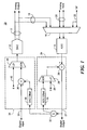
- FIG. 1 An offset calibration system 10 according to this invention for calibrating a digital to analog converter (DAC) 12 and an analog to digital converter (ADC) 14 when the ADC and DAC full-scale ranges are not related by a power of two.
- ADC 14 is provided its inputs by a multiplexer 16 which can select from the output 17 of DAC 12, a normal analog input 20, or the zero input 22 (for offset calibration).
- ADC offset compensation circuit 24 At the output of ADC 14 is ADC offset compensation circuit 24 which includes an adder 26 that receives the output from ADC 14 and the output from multiplexer 28.
- a register 30 is used to store the ADC offset which is determined by the offset compensation circuit 24.
- Register 30 provides the ADC offset to one input of multiplexer 28; the other input 29 to multiplexer 28 is the zero code for calibration mode.
- a range adjustment circuit 32 according to this invention is interconnected between the digital output from adder 26 and the input to the DAC offset compensation circuit 34 associated with DAC 12.
- Offset compensation circuit 34 also includes an adder 36 and a register 38 for storing the DAC offset.
- Adder 36 receives one input from register 38, the other is the digital input on line 35.
- Adder 36 provides one input to multiplexer 40; the other input is the zero input 42 used for calibration.
- the output of multiplexer 40 is delivered to the input of DAC 12.
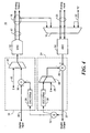
- ADC 14 is calibrated as shown in Fig. 2 by applying a zero input from line 22 to its differential input. Any signal other than zero at the output of ADC 14 is fed through adder 26, to range adjustment circuit 32. The zero input on line 29 to multiplexer 28 is selected so that zero is fed into the negative input of adder 26. Thus, the output of adder 26 represents the ADC offset. The output of adder 26 is delivered through range adjustment circuit 32 to offset compensation circuit 24.
- the value stored in ADC offset register 30 is the offset error produced by ADC 14. During normal operation, the value stored in ADC offset register 30 will be directed through multiplexer 28 into adder 26 where it will be subtracted from to the output of ADC 14 to remove the offset error. During the ADC calibration in Fig. 2, the DAC circuit is not activated.
- a zero input on line 42 through multiplexer 40 is delivered to DAC 12.
- the output of DAC 12 which ideally is zero but is typically some offset error value, is delivered on line 18 through multiplexer 16 to the input of ADC 14.
- the output of ADC 14 now is offset compensated by subtraction of the value in ADC offset register 30 delivered through multiplexer 28 to adder 26.
- the output 27 is delivered through range adjustment circuit 32 to offset compensation circuit 34 of DAC 12.
- whatever offset has occurred will be stored in DAC offset register 38 and in the future will be applied to adder 36 to subtract from the digital input to compensate for the offset of DAC 12.
- the analog input on lines 20 to multiplexer 16 is delivered to ADC 14.
- the output from ADC 14 is compensated by offset compensation circuit 24. This is done by the ADC offset stored in register 30 being delivered through multiplexer 28 to adder 26 where it is subtracted from the output of ADC 14 to remove the ADC offset error.
- adder 36 subtracts the DAC offset stored in register 38 from the digital input signal on line 35 and provides an anticipatory correction to the signal delivered to DAC 12 through multiplexer 40 so that the DAC offset error is compensated and the output on lines 17 is without offset error.
- the range adjustment circuit 32 is employed to introduce the necessary factor so that the offset compensation is accurately accomplished even though DAC 12 and ADC 14 have full-scale ranges that are not related by a power of two.
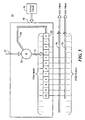
- Range adjustment circuit 32 is shown in more detail in Fig. 5 as including an accumulator 48 having an accumulation register 50 and adder 52. Accumulator 48 and accumulator register 50 act as a filter in normal operation. Control circuit 54 determines how many output values from ADC 14 will be accumulated in register 50.
- the output lines 70 and 72 are the means for selecting the stages of the register representing the quotient of the division of the accumulated values by the preselected power of 2. For example, if the DAC 12 has an output range of ⁇ 1 volt and ADC 14 has a range of ⁇ 1.2 volts, there is an obvious mismatch between the ranges that will affect the accuracy of the DAC offset error compensation.
- a number of successive output values from ADC 14 will be accumulated in register 50 through the use of adder 52 which receives an input on line 27 from ADC 14 through adder 26 and an input on line 56 from register 50.
- the number of values to be accumulated is designated M.
- M A D C range / 2 A D A C range / 2 D * ( 2 n )
- the ADCrange is the ADC full-scale range
- A is the resolution of the ADC (number of bits)
- DACrange is the DAC full-scale range
- D the resolution of the DAC (number of bits)
- 2 n represents some preselected power of 2 chosen for convenience.
- the difference between the full-scale ranges, 1.2 volts and 1 volt, is compensated for by the difference in the accumulation cycles, nineteen and sixteen.
- the ratio of the ADC range to the DAC range is approximately equal or may be made almost exactly equal to the ratio of the number of accumulations for the ADC, M, to the number represented by 2 n .
- the number of output values accumulated in register 50 is determined by control circuit 54. In this case it designates sixteen for the ADC cycle and nineteen for the DAC cycle.
- ADC 14 is a delta-sigma ADC comprising a modulator and a digital filter.
- the digital filter implementation requires an accumulator.
- the logic used to implement the accumulator for the digital filter is also used to implement the range adjustment circuit.
Landscapes
- Engineering & Computer Science (AREA)
- Theoretical Computer Science (AREA)
- Analogue/Digital Conversion (AREA)
- Measuring Pulse, Heart Rate, Blood Pressure Or Blood Flow (AREA)
- Steroid Compounds (AREA)
- Analysing Materials By The Use Of Radiation (AREA)
- Control Of Motors That Do Not Use Commutators (AREA)
Claims (4)
- Ein Offsetkalibrationssystem (10), aufweisend:Einen Analog/Digital-Wandler (14) mit einer ersten Offsetkompensationsschaltung (24); einen Digital/Analog-Wandler (12) mit einer zweiten Offsetkompensationsschaltung (34), wobei der Ausgang besagten Digital/Analog-Wandlers (12) mit dem Eingang besagten Analog/Digital-Wandlers (14) während der Offsetkalibration besagten Digital/Analog-Wandlers (12) verbunden ist, undeine Anpassungsschaltung (32)wobei das Offsetkalibrationssystem (10) gekennzeichnet ist durch:Der Analog/Digital-Wandler (14) hat einen ersten vollständigen Bereich;der Digital/Analog-Wandler (12) hat einen zweiten vollständigen Bereich;
unddie Anpassungsschaltung (32) ist eine Bereichseinstellungsschaltung um eine vorbestimmte Anzahl von Analog/Digital-Ausgangswerten zu akkumulieren und die akkumulierten Werte durch eine vorgewählte Potenz von 2 im Verhältnis der Spannung, die dem kleinstwertigen Bit des Analog/Digital-Wandlers entspricht, und der Spannung, die dem kleinstwertigen Bit des Digital/Analog-Wandlers entspricht, zu teilen. - Das Offsetkalibrationssystem des Anspruchs 1, in dem besagte Bereichseinstellungsschaltung (32) eine Akkumulatorschaltung (48), um besagte vorbestimmte Anzahl von Analog/Digital-Ausgangswerten aufzunehmen, aufweist.
- Das Offsetkalibrationssystem des Anspruchs 2, in dem besagte Akkumulatorschaltung (48) eine Steuerschaltung (54) zum Bestimmen der Anzahl der Analog zu Digtal-Ausgangswerte, die akkumuliert werden sollen, aufweist.
- Das Offsetkalibrationssystem des Anspruchs 2, in dem besagten Akkumulatorschaltung (48) ein Register (50) und Einrichtungen (70, 72) zum Wählen der Stufen des Registers, die den Quotienten der Division der akkumulierten Werte durch besagte vorgewählte Potenz von 2 darstellen, aufweist.
Applications Claiming Priority (3)
| Application Number | Priority Date | Filing Date | Title |
|---|---|---|---|
| US156365 | 2002-05-28 | ||
| US10/156,365 US6624772B1 (en) | 2002-05-28 | 2002-05-28 | Offset calibration system |
| PCT/US2003/011853 WO2003103150A1 (en) | 2002-05-28 | 2003-04-17 | Offset calibration system |
Publications (3)
| Publication Number | Publication Date |
|---|---|
| EP1510007A1 EP1510007A1 (de) | 2005-03-02 |
| EP1510007A4 EP1510007A4 (de) | 2005-07-27 |
| EP1510007B1 true EP1510007B1 (de) | 2006-10-11 |
Family
ID=28041200
Family Applications (1)
| Application Number | Title | Priority Date | Filing Date |
|---|---|---|---|
| EP03731031A Expired - Lifetime EP1510007B1 (de) | 2002-05-28 | 2003-04-17 | Offsetkalibrationssystem |
Country Status (6)
| Country | Link |
|---|---|
| US (1) | US6624772B1 (de) |
| EP (1) | EP1510007B1 (de) |
| CN (1) | CN100426675C (de) |
| AT (1) | ATE342610T1 (de) |
| DE (1) | DE60309025T2 (de) |
| WO (1) | WO2003103150A1 (de) |
Families Citing this family (15)
| Publication number | Priority date | Publication date | Assignee | Title |
|---|---|---|---|---|
| DE10211075A1 (de) * | 2002-03-13 | 2003-10-16 | Siemens Ag | Geregelte Ansteuerschaltung für einen analog angesteuerten Leistungshalbleiter |
| SE521575C2 (sv) * | 2002-03-25 | 2003-11-11 | Ericsson Telefon Ab L M | Kalibrering av A/D omvandlare |
| US6919833B2 (en) * | 2003-09-04 | 2005-07-19 | Regan N. Mills | Parallel converter topology for reducing non-linearity errors |
| US7151475B2 (en) * | 2004-08-31 | 2006-12-19 | Micron Technology, Inc. | Minimized differential SAR-type column-wide ADC for CMOS image sensors |
| US7221298B1 (en) * | 2005-12-08 | 2007-05-22 | Teradyne, Inc. | Calibration circuitry |
| US7443323B2 (en) * | 2007-01-10 | 2008-10-28 | Freescale Semiconductor, Inc. | Calibrating a digital-to-analog converter |
| CN101295984B (zh) * | 2007-04-27 | 2010-09-01 | 扬智科技股份有限公司 | 用来补偿模拟/数字转换器偏移量的偏移补偿电路 |
| JP2010093683A (ja) * | 2008-10-10 | 2010-04-22 | Nec Electronics Corp | デジタルアナログ変換回路とその出力データの補正方法 |
| US8068045B2 (en) * | 2010-03-01 | 2011-11-29 | Analog Devices, Inc. | Calibration methods and structures for pipelined converter systems |
| CN101951262B (zh) * | 2010-09-03 | 2013-09-18 | 英特格灵芯片(天津)有限公司 | Dac校准电路及校准方法 |
| CN102025374B (zh) * | 2010-12-24 | 2013-10-16 | 北京东方计量测试研究所 | 数模转换器的差分非线性误差实时校正的自动校准电路 |
| US8723707B2 (en) | 2011-11-14 | 2014-05-13 | Analog Devices, Inc. | Correlation-based background calibration for reducing inter-stage gain error and non-linearity in pipelined analog-to-digital converters |
| CN104303420B (zh) * | 2012-05-30 | 2017-12-26 | 英特尔公司 | 模数转换器 |
| US9007242B2 (en) * | 2013-06-27 | 2015-04-14 | Realtek Semiconductor Corp. | Self-calibrated delta-sigma modulator and method thereof |
| TWI640778B (zh) * | 2018-03-02 | 2018-11-11 | National Applied Research Laboratories | 訊號誤差校正方法 |
Family Cites Families (19)
| Publication number | Priority date | Publication date | Assignee | Title |
|---|---|---|---|---|
| JPS5953727B2 (ja) * | 1977-04-06 | 1984-12-26 | 株式会社日立製作所 | 補正回路付da変換器 |
| US4509037A (en) * | 1981-06-12 | 1985-04-02 | Gould Inc. | Enhanced delta modulation encoder |
| US4943807A (en) | 1988-04-13 | 1990-07-24 | Crystal Semiconductor | Digitally calibrated delta-sigma analog-to-digital converter |
| US5153593A (en) * | 1990-04-26 | 1992-10-06 | Hughes Aircraft Company | Multi-stage sigma-delta analog-to-digital converter |
| US5248970A (en) | 1991-11-08 | 1993-09-28 | Crystal Semiconductor Corp. | Offset calibration of a dac using a calibrated adc |
| US5583501A (en) * | 1994-08-24 | 1996-12-10 | Crystal Semiconductor Corporation | Digital-to-analog converter with digital linearity correction |
| US5592508A (en) * | 1994-09-22 | 1997-01-07 | Cooper; J. Carl | Analog signal coding and transmission apparatus and method capable of operation with multiple types of analog and digital signals |
| US5796361A (en) * | 1996-09-25 | 1998-08-18 | Exar Corporation | CCD signal digitizing integrated circuit |
| US5793319A (en) * | 1996-11-29 | 1998-08-11 | Ricoh Company, Ltd. | Analog to digital linearizing apparatus, system and method |
| US5982313A (en) * | 1997-06-06 | 1999-11-09 | Analog Devices, Inc. | High speed sigma-delta analog-to-digital converter system |
| US5905453A (en) * | 1997-08-04 | 1999-05-18 | Motorola, Inc. | Dithered sigma delta modulator having programmable full scale range adjustment |
| US5977894A (en) * | 1997-12-31 | 1999-11-02 | Maxim Integrated Products, Inc. | Digital calibration for analog-to-digital converters with implicit gain proration |
| US6459426B1 (en) * | 1998-08-17 | 2002-10-01 | Genesis Microchip (Delaware) Inc. | Monolithic integrated circuit implemented in a digital display unit for generating digital data elements from an analog display signal received at high frequencies |
| US6351228B1 (en) * | 1999-02-03 | 2002-02-26 | Hitachi Electronics Engineering Co., Ltd. | Digital calibration method and apparatus for A/D or D/A converters |
| US6281818B1 (en) * | 1999-05-14 | 2001-08-28 | Diamond Systems Corporation | Automatic auto-calibration system |
| US6229466B1 (en) * | 1999-08-23 | 2001-05-08 | Level One Communications, Inc. | Digital calibration method and apparatus for multi-bit delta-sigma D/A converter |
| US6417794B1 (en) * | 1999-09-09 | 2002-07-09 | Cirrus Logic, Inc. | System and apparatus for digitally calibrating capacitors in an analog-to-digital converter using successive approximation |
| US6424276B1 (en) * | 1999-09-09 | 2002-07-23 | Cirrus Logic, Inc. | Successive approximation algorithm-based architectures and systems |
| US6323800B1 (en) * | 2000-02-17 | 2001-11-27 | Advanced Micro Devices, Inc. | Pipeline analog to digital (a/d) converter with lengthened hold operation of a first stage |
-
2002
- 2002-05-28 US US10/156,365 patent/US6624772B1/en not_active Expired - Lifetime
-
2003
- 2003-04-17 EP EP03731031A patent/EP1510007B1/de not_active Expired - Lifetime
- 2003-04-17 DE DE60309025T patent/DE60309025T2/de not_active Expired - Lifetime
- 2003-04-17 CN CNB03814719XA patent/CN100426675C/zh not_active Expired - Lifetime
- 2003-04-17 AT AT03731031T patent/ATE342610T1/de not_active IP Right Cessation
- 2003-04-17 WO PCT/US2003/011853 patent/WO2003103150A1/en not_active Ceased
Also Published As
| Publication number | Publication date |
|---|---|
| EP1510007A1 (de) | 2005-03-02 |
| CN100426675C (zh) | 2008-10-15 |
| DE60309025D1 (de) | 2006-11-23 |
| US6624772B1 (en) | 2003-09-23 |
| ATE342610T1 (de) | 2006-11-15 |
| EP1510007A4 (de) | 2005-07-27 |
| DE60309025T2 (de) | 2007-05-24 |
| CN1663127A (zh) | 2005-08-31 |
| WO2003103150A1 (en) | 2003-12-11 |
Similar Documents
| Publication | Publication Date | Title |
|---|---|---|
| EP1510007B1 (de) | Offsetkalibrationssystem | |
| US5598157A (en) | Sigma Delta analog to digital converter with three point calibration apparatus and method | |
| US9041569B2 (en) | Method and apparatus for calibration of successive approximation register analog-to-digital converters | |
| US7501965B2 (en) | Correcting for errors that cause generated digital codes to deviate from expected values in an ADC | |
| US5644308A (en) | Algorithmic analog-to-digital converter having redundancy and digital calibration | |
| US10840934B2 (en) | Methods and apparatus for a successive approximation register analog-to-digital converter | |
| US7378999B1 (en) | Method and apparatus for digital calibration of an analog-to-digital converter | |
| US4896155A (en) | Method and apparatus for self-calibration of subranging A/D converter | |
| EP0698315B1 (de) | Algorithmischer analog-/digitalwandler mit digital kalibriertem ausgang | |
| US4746903A (en) | Parallel algorithmic digital to analog converter | |
| EP0616433A1 (de) | Auf die Statistik basiertes kontinuierliches Autokalibrierungsverfahren und -gerät | |
| EP0730794B1 (de) | Effiziente architektur zur korrektur von komponentenfehlanpassungen und schaltungsnichtlinearitäten in a/d umsetzern | |
| US6456223B1 (en) | Pipelined analog to digital converter using digital mismatch noise cancellation | |
| GB1577007A (en) | Conversion system with compensation circuit | |
| US8207882B1 (en) | Analog-to-digital converter (ADC) having a folding stage and multiple ADC stages | |
| EP3637619B1 (de) | Signalverarbeitung und -umsetzung | |
| EP0078687B1 (de) | Analog-Digital-Wandler | |
| JPH1048293A (ja) | 半導体試験装置 | |
| JP4947899B2 (ja) | デジタル補正集積回路およびデジタルアナログコンバータ(dac) | |
| US5838598A (en) | Method and apparatus for gain correction of a sigma-delta converter | |
| TWI400887B (zh) | 類比數位轉換器 | |
| KR20060048454A (ko) | A/d 변환 장치, 및 이를 이용한 통신 기기 | |
| JP3130007B2 (ja) | 逐次比較型a/dコンバータ回路 | |
| US6392578B1 (en) | Digital-to-analog converter and a method for facilitating outputting of an analog output of predetermined value from the digital-to-analog converter in response to a digital input code | |
| KR20020014522A (ko) | 에러 보정이 가능한 연속 근사 레지스터 타입의아날로그-디지털 변환 장치 및 에러 보정 방법 |
Legal Events
| Date | Code | Title | Description |
|---|---|---|---|
| PUAI | Public reference made under article 153(3) epc to a published international application that has entered the european phase |
Free format text: ORIGINAL CODE: 0009012 |
|
| 17P | Request for examination filed |
Effective date: 20041123 |
|
| AK | Designated contracting states |
Kind code of ref document: A1 Designated state(s): AT BE BG CH CY CZ DE DK EE ES FI FR GB GR HU IE IT LI LU MC NL PT RO SE SI SK TR |
|
| A4 | Supplementary search report drawn up and despatched |
Effective date: 20050615 |
|
| GRAP | Despatch of communication of intention to grant a patent |
Free format text: ORIGINAL CODE: EPIDOSNIGR1 |
|
| GRAS | Grant fee paid |
Free format text: ORIGINAL CODE: EPIDOSNIGR3 |
|
| GRAA | (expected) grant |
Free format text: ORIGINAL CODE: 0009210 |
|
| AK | Designated contracting states |
Kind code of ref document: B1 Designated state(s): AT BE BG CH CY CZ DE DK EE ES FI FR GB GR HU IE IT LI LU MC NL PT RO SE SI SK TR |
|
| PG25 | Lapsed in a contracting state [announced via postgrant information from national office to epo] |
Ref country code: FI Free format text: LAPSE BECAUSE OF FAILURE TO SUBMIT A TRANSLATION OF THE DESCRIPTION OR TO PAY THE FEE WITHIN THE PRESCRIBED TIME-LIMIT Effective date: 20061011 Ref country code: IT Free format text: LAPSE BECAUSE OF FAILURE TO SUBMIT A TRANSLATION OF THE DESCRIPTION OR TO PAY THE FEE WITHIN THE PRESCRIBED TIME-LIMIT;WARNING: LAPSES OF ITALIAN PATENTS WITH EFFECTIVE DATE BEFORE 2007 MAY HAVE OCCURRED AT ANY TIME BEFORE 2007. THE CORRECT EFFECTIVE DATE MAY BE DIFFERENT FROM THE ONE RECORDED. Effective date: 20061011 Ref country code: CZ Free format text: LAPSE BECAUSE OF FAILURE TO SUBMIT A TRANSLATION OF THE DESCRIPTION OR TO PAY THE FEE WITHIN THE PRESCRIBED TIME-LIMIT Effective date: 20061011 Ref country code: RO Free format text: LAPSE BECAUSE OF FAILURE TO SUBMIT A TRANSLATION OF THE DESCRIPTION OR TO PAY THE FEE WITHIN THE PRESCRIBED TIME-LIMIT Effective date: 20061011 Ref country code: SK Free format text: LAPSE BECAUSE OF FAILURE TO SUBMIT A TRANSLATION OF THE DESCRIPTION OR TO PAY THE FEE WITHIN THE PRESCRIBED TIME-LIMIT Effective date: 20061011 Ref country code: LI Free format text: LAPSE BECAUSE OF FAILURE TO SUBMIT A TRANSLATION OF THE DESCRIPTION OR TO PAY THE FEE WITHIN THE PRESCRIBED TIME-LIMIT Effective date: 20061011 Ref country code: CH Free format text: LAPSE BECAUSE OF FAILURE TO SUBMIT A TRANSLATION OF THE DESCRIPTION OR TO PAY THE FEE WITHIN THE PRESCRIBED TIME-LIMIT Effective date: 20061011 Ref country code: NL Free format text: LAPSE BECAUSE OF FAILURE TO SUBMIT A TRANSLATION OF THE DESCRIPTION OR TO PAY THE FEE WITHIN THE PRESCRIBED TIME-LIMIT Effective date: 20061011 Ref country code: AT Free format text: LAPSE BECAUSE OF FAILURE TO SUBMIT A TRANSLATION OF THE DESCRIPTION OR TO PAY THE FEE WITHIN THE PRESCRIBED TIME-LIMIT Effective date: 20061011 Ref country code: SI Free format text: LAPSE BECAUSE OF FAILURE TO SUBMIT A TRANSLATION OF THE DESCRIPTION OR TO PAY THE FEE WITHIN THE PRESCRIBED TIME-LIMIT Effective date: 20061011 Ref country code: BE Free format text: LAPSE BECAUSE OF FAILURE TO SUBMIT A TRANSLATION OF THE DESCRIPTION OR TO PAY THE FEE WITHIN THE PRESCRIBED TIME-LIMIT Effective date: 20061011 |
|
| REG | Reference to a national code |
Ref country code: GB Ref legal event code: FG4D |
|
| REG | Reference to a national code |
Ref country code: CH Ref legal event code: EP |
|
| REG | Reference to a national code |
Ref country code: IE Ref legal event code: FG4D |
|
| REF | Corresponds to: |
Ref document number: 60309025 Country of ref document: DE Date of ref document: 20061123 Kind code of ref document: P |
|
| PG25 | Lapsed in a contracting state [announced via postgrant information from national office to epo] |
Ref country code: SE Free format text: LAPSE BECAUSE OF FAILURE TO SUBMIT A TRANSLATION OF THE DESCRIPTION OR TO PAY THE FEE WITHIN THE PRESCRIBED TIME-LIMIT Effective date: 20070111 Ref country code: BG Free format text: LAPSE BECAUSE OF FAILURE TO SUBMIT A TRANSLATION OF THE DESCRIPTION OR TO PAY THE FEE WITHIN THE PRESCRIBED TIME-LIMIT Effective date: 20070111 Ref country code: DK Free format text: LAPSE BECAUSE OF FAILURE TO SUBMIT A TRANSLATION OF THE DESCRIPTION OR TO PAY THE FEE WITHIN THE PRESCRIBED TIME-LIMIT Effective date: 20070111 |
|
| PG25 | Lapsed in a contracting state [announced via postgrant information from national office to epo] |
Ref country code: ES Free format text: LAPSE BECAUSE OF FAILURE TO SUBMIT A TRANSLATION OF THE DESCRIPTION OR TO PAY THE FEE WITHIN THE PRESCRIBED TIME-LIMIT Effective date: 20070122 |
|
| PG25 | Lapsed in a contracting state [announced via postgrant information from national office to epo] |
Ref country code: PT Free format text: LAPSE BECAUSE OF FAILURE TO SUBMIT A TRANSLATION OF THE DESCRIPTION OR TO PAY THE FEE WITHIN THE PRESCRIBED TIME-LIMIT Effective date: 20070319 |
|
| NLV1 | Nl: lapsed or annulled due to failure to fulfill the requirements of art. 29p and 29m of the patents act | ||
| REG | Reference to a national code |
Ref country code: CH Ref legal event code: PL |
|
| ET | Fr: translation filed | ||
| PLBE | No opposition filed within time limit |
Free format text: ORIGINAL CODE: 0009261 |
|
| STAA | Information on the status of an ep patent application or granted ep patent |
Free format text: STATUS: NO OPPOSITION FILED WITHIN TIME LIMIT |
|
| 26N | No opposition filed |
Effective date: 20070712 |
|
| REG | Reference to a national code |
Ref country code: GB Ref legal event code: 732E |
|
| PG25 | Lapsed in a contracting state [announced via postgrant information from national office to epo] |
Ref country code: GR Free format text: LAPSE BECAUSE OF FAILURE TO SUBMIT A TRANSLATION OF THE DESCRIPTION OR TO PAY THE FEE WITHIN THE PRESCRIBED TIME-LIMIT Effective date: 20070112 |
|
| PG25 | Lapsed in a contracting state [announced via postgrant information from national office to epo] |
Ref country code: IE Free format text: LAPSE BECAUSE OF NON-PAYMENT OF DUE FEES Effective date: 20070417 |
|
| PG25 | Lapsed in a contracting state [announced via postgrant information from national office to epo] |
Ref country code: EE Free format text: LAPSE BECAUSE OF FAILURE TO SUBMIT A TRANSLATION OF THE DESCRIPTION OR TO PAY THE FEE WITHIN THE PRESCRIBED TIME-LIMIT Effective date: 20061011 |
|
| PG25 | Lapsed in a contracting state [announced via postgrant information from national office to epo] |
Ref country code: MC Free format text: LAPSE BECAUSE OF NON-PAYMENT OF DUE FEES Effective date: 20070430 |
|
| PG25 | Lapsed in a contracting state [announced via postgrant information from national office to epo] |
Ref country code: LU Free format text: LAPSE BECAUSE OF NON-PAYMENT OF DUE FEES Effective date: 20070417 Ref country code: CY Free format text: LAPSE BECAUSE OF FAILURE TO SUBMIT A TRANSLATION OF THE DESCRIPTION OR TO PAY THE FEE WITHIN THE PRESCRIBED TIME-LIMIT Effective date: 20061011 |
|
| PG25 | Lapsed in a contracting state [announced via postgrant information from national office to epo] |
Ref country code: HU Free format text: LAPSE BECAUSE OF FAILURE TO SUBMIT A TRANSLATION OF THE DESCRIPTION OR TO PAY THE FEE WITHIN THE PRESCRIBED TIME-LIMIT Effective date: 20070412 Ref country code: TR Free format text: LAPSE BECAUSE OF FAILURE TO SUBMIT A TRANSLATION OF THE DESCRIPTION OR TO PAY THE FEE WITHIN THE PRESCRIBED TIME-LIMIT Effective date: 20061011 |
|
| REG | Reference to a national code |
Ref country code: DE Ref legal event code: R082 Ref document number: 60309025 Country of ref document: DE Representative=s name: SAMSON & PARTNER PATENTANWAELTE MBB, DE |
|
| REG | Reference to a national code |
Ref country code: FR Ref legal event code: PLFP Year of fee payment: 14 |
|
| REG | Reference to a national code |
Ref country code: FR Ref legal event code: PLFP Year of fee payment: 15 |
|
| REG | Reference to a national code |
Ref country code: FR Ref legal event code: PLFP Year of fee payment: 16 |
|
| PGFP | Annual fee paid to national office [announced via postgrant information from national office to epo] |
Ref country code: GB Payment date: 20220427 Year of fee payment: 20 Ref country code: FR Payment date: 20220425 Year of fee payment: 20 Ref country code: DE Payment date: 20220427 Year of fee payment: 20 |
|
| REG | Reference to a national code |
Ref country code: DE Ref legal event code: R071 Ref document number: 60309025 Country of ref document: DE |
|
| REG | Reference to a national code |
Ref country code: GB Ref legal event code: PE20 Expiry date: 20230416 |
|
| PG25 | Lapsed in a contracting state [announced via postgrant information from national office to epo] |
Ref country code: GB Free format text: LAPSE BECAUSE OF EXPIRATION OF PROTECTION Effective date: 20230416 |