EP1510009B1 - Procede d'etalonnage d'un convertisseur numerique-analogique et convertisseur numerique-analogique - Google Patents
Procede d'etalonnage d'un convertisseur numerique-analogique et convertisseur numerique-analogique Download PDFInfo
- Publication number
- EP1510009B1 EP1510009B1 EP02724361A EP02724361A EP1510009B1 EP 1510009 B1 EP1510009 B1 EP 1510009B1 EP 02724361 A EP02724361 A EP 02724361A EP 02724361 A EP02724361 A EP 02724361A EP 1510009 B1 EP1510009 B1 EP 1510009B1
- Authority
- EP
- European Patent Office
- Prior art keywords
- digital
- deviation
- sorting
- dac
- current sources
- Prior art date
- Legal status (The legal status is an assumption and is not a legal conclusion. Google has not performed a legal analysis and makes no representation as to the accuracy of the status listed.)
- Expired - Lifetime
Links
- 238000000034 method Methods 0.000 title claims description 48
- 238000013507 mapping Methods 0.000 claims description 69
- 238000003491 array Methods 0.000 claims description 16
- 238000004590 computer program Methods 0.000 claims 2
- 238000004422 calculation algorithm Methods 0.000 description 19
- 238000013461 design Methods 0.000 description 10
- 238000009826 distribution Methods 0.000 description 10
- 230000006399 behavior Effects 0.000 description 9
- 238000010586 diagram Methods 0.000 description 9
- 230000009897 systematic effect Effects 0.000 description 6
- 230000001965 increasing effect Effects 0.000 description 5
- 238000005259 measurement Methods 0.000 description 5
- 230000007423 decrease Effects 0.000 description 4
- 230000003247 decreasing effect Effects 0.000 description 4
- 238000006243 chemical reaction Methods 0.000 description 3
- 230000000694 effects Effects 0.000 description 3
- 230000006870 function Effects 0.000 description 3
- 239000011159 matrix material Substances 0.000 description 3
- 238000013139 quantization Methods 0.000 description 3
- 238000012935 Averaging Methods 0.000 description 2
- 238000005516 engineering process Methods 0.000 description 2
- 238000012545 processing Methods 0.000 description 2
- 238000005070 sampling Methods 0.000 description 2
- 230000015572 biosynthetic process Effects 0.000 description 1
- 238000004364 calculation method Methods 0.000 description 1
- 230000001413 cellular effect Effects 0.000 description 1
- 238000004891 communication Methods 0.000 description 1
- 230000000295 complement effect Effects 0.000 description 1
- 238000012937 correction Methods 0.000 description 1
- 230000001419 dependent effect Effects 0.000 description 1
- 229920005994 diacetyl cellulose Polymers 0.000 description 1
- 230000002708 enhancing effect Effects 0.000 description 1
- 238000003384 imaging method Methods 0.000 description 1
- 238000004088 simulation Methods 0.000 description 1
- 239000000758 substrate Substances 0.000 description 1
- 238000003786 synthesis reaction Methods 0.000 description 1
- 238000012360 testing method Methods 0.000 description 1
- 238000009966 trimming Methods 0.000 description 1
Images


Classifications
-
- H—ELECTRICITY
- H03—ELECTRONIC CIRCUITRY
- H03M—CODING; DECODING; CODE CONVERSION IN GENERAL
- H03M1/00—Analogue/digital conversion; Digital/analogue conversion
- H03M1/66—Digital/analogue converters
- H03M1/70—Automatic control for modifying converter range
-
- H—ELECTRICITY
- H03—ELECTRONIC CIRCUITRY
- H03M—CODING; DECODING; CODE CONVERSION IN GENERAL
- H03M1/00—Analogue/digital conversion; Digital/analogue conversion
- H03M1/06—Continuously compensating for, or preventing, undesired influence of physical parameters
- H03M1/0617—Continuously compensating for, or preventing, undesired influence of physical parameters characterised by the use of methods or means not specific to a particular type of detrimental influence
- H03M1/0634—Continuously compensating for, or preventing, undesired influence of physical parameters characterised by the use of methods or means not specific to a particular type of detrimental influence by averaging out the errors, e.g. using sliding scale
- H03M1/0643—Continuously compensating for, or preventing, undesired influence of physical parameters characterised by the use of methods or means not specific to a particular type of detrimental influence by averaging out the errors, e.g. using sliding scale in the spatial domain
- H03M1/0651—Continuously compensating for, or preventing, undesired influence of physical parameters characterised by the use of methods or means not specific to a particular type of detrimental influence by averaging out the errors, e.g. using sliding scale in the spatial domain by selecting the quantisation value generators in a non-sequential order, e.g. symmetrical
-
- H—ELECTRICITY
- H03—ELECTRONIC CIRCUITRY
- H03M—CODING; DECODING; CODE CONVERSION IN GENERAL
- H03M1/00—Analogue/digital conversion; Digital/analogue conversion
- H03M1/10—Calibration or testing
-
- H—ELECTRICITY
- H03—ELECTRONIC CIRCUITRY
- H03M—CODING; DECODING; CODE CONVERSION IN GENERAL
- H03M1/00—Analogue/digital conversion; Digital/analogue conversion
- H03M1/10—Calibration or testing
- H03M1/1009—Calibration
- H03M1/1033—Calibration over the full range of the converter, e.g. for correcting differential non-linearity
-
- H—ELECTRICITY
- H03—ELECTRONIC CIRCUITRY
- H03M—CODING; DECODING; CODE CONVERSION IN GENERAL
- H03M1/00—Analogue/digital conversion; Digital/analogue conversion
- H03M1/66—Digital/analogue converters
- H03M1/68—Digital/analogue converters with conversions of different sensitivity, i.e. one conversion relating to the more significant digital bits and another conversion to the less significant bits
- H03M1/682—Digital/analogue converters with conversions of different sensitivity, i.e. one conversion relating to the more significant digital bits and another conversion to the less significant bits both converters being of the unary decoded type
-
- H—ELECTRICITY
- H03—ELECTRONIC CIRCUITRY
- H03M—CODING; DECODING; CODE CONVERSION IN GENERAL
- H03M1/00—Analogue/digital conversion; Digital/analogue conversion
- H03M1/66—Digital/analogue converters
- H03M1/68—Digital/analogue converters with conversions of different sensitivity, i.e. one conversion relating to the more significant digital bits and another conversion to the less significant bits
- H03M1/687—Segmented, i.e. the more significant bit converter being of the unary decoded type and the less significant bit converter being of the binary weighted type
-
- H—ELECTRICITY
- H03—ELECTRONIC CIRCUITRY
- H03M—CODING; DECODING; CODE CONVERSION IN GENERAL
- H03M1/00—Analogue/digital conversion; Digital/analogue conversion
- H03M1/66—Digital/analogue converters
- H03M1/74—Simultaneous conversion
- H03M1/742—Simultaneous conversion using current sources as quantisation value generators
- H03M1/747—Simultaneous conversion using current sources as quantisation value generators with equal currents which are switched by unary decoded digital signals
Definitions
- the present invention relates to integrated electronic circuits.
- the present invention relates to a novel and improved method for calibrating an unweighted current source array of a segmented current-steering D/A-converter and to a novel and improved D/A-converter design implementing said calibration method.
- Digital-to-analog converters are widely used for converting digital signals to corresponding analog signals for many electronic circuits.
- a high resolution, high speed digital-to-analog converter may find applications in cellular base stations, wireless communications, direct digital frequency synthesis, signal reconstruction, test equipment, high resolution imaging systems and arbitrary waveform generators, for example.
- the high-resolution (>10 bit) current-steering D/A-converters are typically divided into two or more different subsets, so that each of the subsets makes a conversion of some of the input bits from digital signal into an analog current.
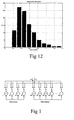
- An example of such a topology is shown in figure 1.
- the MSB-subset is the most critical because it converts the most significant bits, and therefore most of the output signal.
- the MSB-block or subset is a matrix of unweighted current sources that are controlled by thermometer decoded input bits. This means that for example 6 MSB's are thermometer decoded into 63 control signals which control the 63 differential current switches. Because one of the 64 signal levels that 6-bit binary word (2 6 ) can point is 0, only 63 signals are needed.
- the LSB-block has typically binary-weighted current sources that are controlled by the LSB's without any decoding. In addition to that, there can be a middle bit conversion that can be both binary-weighted or unweighted.
- the DC-linearity of the current steering DAC is mainly affected by the matching of the current source transistors in the MSB subset.
- a and A vth are the process dependent variables.
- W and L are the width and the length of the current source transistor, respectively, and V gs is the gate-source voltage of the transistor.
- the switching order of the current source array is typically selected so that the cumulating of the systematic errors are evenly spread over the full ramp signal.
- One of the most common methods is symmetrical switching.
- the switching order randomising affects only the systematic error cumulating.
- the shape of the cumulating error affects the dynamic performance. Especially if the INL curve is heavily bowed, the DC-non-linearity can increase the distortion. On the other hand, the large INL error increases the quantization noise.
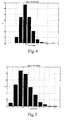
- FIGS 3a and 3b are DNL and INL curves of the unweighted array referred to 14-bit resolution.
- Each of the current sources is described with the following equation. The result is from 1000 Matlab simulations.
- I MSB i I MSB i 0 ⁇ ( 1 + X rand ⁇ ⁇ I d I d ) where X rand is a normally distributed random number.
- I MS00 is the ideal current and ⁇ Id /I d is the standard deviation of the error.
- Figure 4 and figure 5 show the relative distribution of the DNL and INL errors. As shown in figure 5, a typical INL is nearly 12-bit and only 11-bits is achievable with high yield.
- the mismatch of the current sources determines the DC-linearity behaviour of the whole D/A-converter.
- the target is to have both the DNL and the INL values less than 0.5LSB.
- the differential non-linearity (DNL) describes how large the step deviation from 1 LSB is.
- the integral non-linearity (INL) shows the cumulating sum of the errors. Therefore for the sufficient DC-linearity, the mismatch should be small enough so as not to deviate the currents too much from the nominal. Due to the Gaussian distribution nature of the random mismatch, the design margins must be relatively large to guarantee a high yield.
- a non-calibrated high-resolution DAC has typically low or intermediate high frequency behaviour, due to the optimisation for full DC-linearity. Therefore for high-resolution and high-frequency performance, some calibration is highly desired.
- a pseudo calibration method called dynamic element matching is a common method, especially in D/A-converters inside sigma-delta type of data converters.
- the method spreads the linearity errors to the noise floor by continuously changing the order of the switching pattern.
- the actual calibration methods have two main bases, trimming the actual current sources, or having an extra low precision DAC to generate a correction term to the output. These methods need typically a continuous calibration due to the changing conditions. For example temperature or biasing conditions can vary.
- the dynamic element matching method spreads the DC-linearity errors into the noise floor, and therefore the errors still exists even though the distortion is low.
- the SNDR (Signal-to-noise-and-distortion) value is still the same in the frequency band of f sample /2 with or without the dynamic matching method, and therefore the actual effective number of bits does not increase at all.
- US patent 6,118,398 describes a digital-to-analog converter (DAC) which includes a plurality of current sources on a substrate operable in a predetermined sequence of use for generating an output current based upon a digital input, and a connection network for establishing the predetermined sequence of use for the current sources based upon the actual current values and for increasing the performance of the DAC.
- Said connection network can be used to reduce integral non-linearity error of the DAC.
- the connection network may be provided by a plurality of fusible links selectively connected to set the predetermined sequence of use.
- the connection network is, however, connected after the digital part of the whole converter and is thus located on the analog side. This makes the design of the analog more complex and remarkably affects the high frequency linearity of the analog side.
- the plurality of the current sources has actual values that can be sorted from lowest to highest, and each actual current value will define an error value with both a magnitude and polarity relative to the desired value.
- One embodiment for sorting the order of use of the current sources is based upon the error values.
- Tesh et al. discloses a digital-to-analog converter (DAC) including a so-called current cell matrix.
- An input word with specific length can be separated into most significant bits (MSB) and least significant bits (LSB) and these words are converted into analog currents with the help of current sources and their controlling means.
- Tesh comprises a first array of current source cells comprising two rows and extending in two directions.
- Tesh comprises two-dimensional symmetrical control means for operating predetermined current source cells based upon a portion of digital input words and in a symmetrical sequence in both directions with respect to the medial position of the first array.
- the two-dimensional symmetrical control means comprises a decoder (typically thermometer decoder), which generates control signals based upon the MSBs.
- the control means operates the first row with even control signals and the second row with odd control signals.
- the LSB current source cells are positioned in medial portion of an array and they may have binarily weighted output currents. Meanwhile, the MSB current source cells form the other parts of the array and their output currents are mutually substantially equal.
- a matrix configuration for the current cells is used.
- the so-called symmetrical switching structure is presented in Miki in order to reduce linearity error.
- Symmetrical switching means that the minimum or maximum current is in the middle of the switching array while the other current values are placed symmetrically around the center of the array. In other words, if there are seven current sources and the current sources are numbered from 1 ... 7 from the smallest value towards the highest value, the symmetrical switching array in Miki is formed as [6, 4, 2, 1, 3, 5, 7].
- High-speed decoding circuit is used and fast settling time is achieved. Maximum conversion rate is achieved by using 80 MHz frequency.
- the purpose or target of the present invention is to decrease the high variation in the INL curves, so that the cumulating of the errors does not generate highly bowed linearity curves.
- moving the maximum deviations near the zero- and full-scale codes the limiting of the signal swing can always decrease the effect of the DC errors from the signal.
- the calibrated INL is always less than without the calibration.
- the object of the present invention is to provide a digital-to-analog converter design in which the improvement of the DC-linearity is achieved with less effects on the AC-linearity.
- the invention describes a method for digitally calibrating a segmented current-steering D/A-converter.
- One embodiment of the present invention is a 14-bit DAC, where 6 MSB's are converted with two unweighted switchable current source array.
- a new method for organising the switching order based on the analysed data of mismatch of the current sources is presented.
- a programmable mapping device is used instead of the fixed thermometer decoding before the switch array. Using this programmable mapping device the switching order of the current switches can be selected optimally so that the error in resulting analog signal is minimised.
- the switching order is programmed to the mapping device on the basis of the calibration method according to the present invention.
- the inventive amendment is aimed at processing errors which cause poor matching inside the component itself. This amendment is done by rearranging the unweighted unity current switches into a more optimum order.
- the present invention discloses a digital-to-analog converter (DAC), which comprises a set of switchable current sources configured to operate in a pre-determined order.
- the present invention is characterised in that the DAC further comprises an analog-to-digital converter (ADC) configured to measure current deviation data in proportion to a reference current from said set of switchable current sources.
- ADC analog-to-digital converter
- the DAC is further characterised in that it comprises a calibration device which is configured to calibrate the DAC.
- the calibration device further comprises a sorting device, which is configured to sort switchable current sources to a switching order in which the positive and negative deviations of the switchable current sources from said reference current compensate each other.
- the DAC is further characterised in that it comprises a mapping device connected to the calibration device, where the mapping device is configured to switch the switchable current sources in the sorted switching order loaded from the sorting device.
- the sorting device of the DAC is further configured to select the switching order so that the largest positive deviation from the reference current is the first, the largest negative deviation from the reference current is the second, the third largest positive deviation from the reference current is the third, the third largest negative deviation from the reference current is the fourth, and so on, wherein the second latest is the second largest negative deviation, and last one is the second largest positive deviation.
- the calibration device is configured to initialise the calibration by loading to said mapping device a piece of mapping data that switches said switchable current sources one by one by comparing them independently to the reference current.
- said set of switchable current sources is divided into two arrays of switchable current sources
- said mapping device is divided into two independent mappers that are connected to said arrays of switchable current sources
- said sorting device is configured to sort a first piece of mapping data for the first array in the first order and a second piece of mapping data for the second array to the reverse order compared to the first order.
- the calibration device further comprises a storing device (RAM) configured to store said current deviation and/or mapping data, and control logic for controlling said sorting device.
- RAM storing device
- the sorting device further comprises a sorting counter configured to save the address values of the deviation data for the mapping device, and a sorting ready counter is configured to control progress of the sorting.
- the sorting device further comprises a read-only memory (ROM) configured to store mapping data for initialisation of said calibration device.
- ROM read-only memory
- the inventive idea also comprises a calibration method for calibrating the digital-to-analog converter (DAC), which uses a set of switchable current sources, in which method said switchable current sources are arranged to operate in a pre-determined order.
- the calibration method is characterised in that current deviation data is measured in proportion to a reference current from said set of switchable current sources with an analog-to-digital converter (ADC).
- ADC analog-to-digital converter
- the calibration method is further characterised in that switchable current sources are sorted to a switching order in which the positive and negative deviations of the switchable current sources from said reference current compensate each other.
- the calibration method is further characterised in that the switching order is loaded to a mapping device as a mapping data for switching the switchable current sources in the sorted switching order.
- the switching order is selected so that the largest positive deviation from the reference current is the first, the largest negative deviation from the reference current is the second, the third largest positive deviation from the reference current is the third, the third largest negative deviation from the reference current is the fourth, and so on, wherein the second latest is the second largest negative deviation, and last one is the second largest positive deviation.
- the calibration is initialised by loading to the mapping device a piece of mapping data that switches the switchable current sources one by one by comparing them independently to the reference current.
- a first piece of mapping data is sorted for the first array in the first order and a second piece of mapping data for the second array is sorted to the reverse order compared to the first order.
- the current deviation and/or mapping data is stored to a storing device, and the sorting device is controlled by control logic.
- the address values of the deviation data are saved for the mapping procedure in a sorting counter, and progress of the sorting is controlled in a sorting ready counter.
- mapping data for initialisation of said calibration device is stored to a read-only memory.
- the new design of the DAC does not have any effect on the analog parts of the current DAC's. Therefore there is no risk of decreasing the dynamic performance of the DAC by implementing the calibration.
- the calibration method according to the present invention does not increase the complexity of the analog part of the DAC since everything is done in the digital part of the DAC.
- the use of the digital calibration method makes it possible to design the DAC to be fully optimised for the high frequency performance. Also the analog area of the DAC can be kept small, which is also an advantage for the high-frequency behaviour.
- the whole calibration algorithm can be implemented with suitable software. If the DAC is a stand-alone chip, the calibration algorithm can be implemented on the same chip, and the DAC can operate as a self calibrating DAC. After the calibration, the calibration logic can be put to a power-down state, and it consumes no current.
- the method according to the present invention calibrates both the random and the systematic errors.
- FIG. 6 a block diagram disclosing a simplified principle example of the switchable current source array 1 that can be calibrated.
- Switchable current source means for example a combination of a current source and a switching element which together form a switchable current source.
- Figure 6 also shows a programmable mapping device 2 which is used instead of the conventional thermometer decoder.
- the mapping device 2 is connected to the current switch array 1 in order to control the switching order of the current switches in the current switch array 1.
- the mapping device can map any of the 6-bit input signals into any combination of the 63 output signals based on the result from the calibration algorithm of the present invention.
- a 63x63 cell RAM is capable of this function.
- the mapping data which is input into the mapping device 2 is based on the calibration algorithm and the data collected by it.
- the calibration algorithm measures the current deviation of the current sources compared to the nominal value. Based on the measurements, the current sources are sorted in the optimal order to minimise the INL deviation. The details of the calibration algorithm are explained later in this application.
- the switching order of the first set of MSB current sources is selected so that the maximum positive and negative deviations from the nominal current are located in the beginning and in the end of the ramp. Every even code has a positive error and every odd code has a negative error. In the middle codes the deviation from the nominal value is at its minimum value. In the second set of MSB current sources every even code has a negative error and every odd code has a positive error.
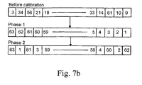
- Figures 7a - b demonstrate the target of the switching order mapping in the embodiment of the two switching arrays.
- Number 1 represents the smallest current (I 0 -I err,max,neg ) and value 63 represents the maximum current (I 0 +I err.max,pos ).
- the calibrated linearity curves of the structure in figure 6 are shown in figures 8a and 8b, respectively.
- the curves are calculated with the same current source data as the non-calibrated curves in figures 3a and 3b.
- a 4-bit quantization is used for the deviation measurement. This basically means that a 4-bit ADC (analog-to-digital converter) could be used for the error measurement. For each run the maximum code deviation is scaled to the maximum error.
- FIG. 9 A block diagram of an improved implementation of the calibration is disclosed in figure 9.
- two parallel switching arrays 1a, 1b are used that both have their own programmable mapping devices or mappers 2a and 2b.
- a switching array means here an array whose elements consist in a current source and a swithc connected to said current source. The current of the arrays are connected together at the top level, so that the unit current is twice the unit current in one array.
- Both arrays 1a and 1b have their own mapping devices 2a and 2b, which are connected to the same digital input signal.
- mapping data 1 and 2 respectively.
- a mapping device which is capable of the required mapping function is a simple RAM (Random Access Memory, RAM) circuit.
- RAM Random Access Memory
- 3969 cells are needed. If the target of the DAC is to operate at the several hundreds of megahertz sampling rate, the 63 x 63 bit RAM is not optimal. There is a possibility to reduce the number of cells. To improve the performance, the RAM can be divided into column and row units, as shown in figure 13. If this kind of row/column configuration is in use, the addresses of the mapping device RAM in the calibration algorithm should also be row column addressed.
- the column banks are 63 x 4 bit RAM circuits that get the 6 MSB's of the input data and map their output to the row banks. For each of the 6-bit input code there is an address value for the row RAM that tells how many switches there are to be switched from the selected column. The zero value express that no cells are switched from the column.
- the 8 x 8 bit RAM row banks map the switching order of the elements or cells in each of the columns. For each 8 address code from the column bank, there is a unique 8-bit word that switches one more switch cells compared to the previous word. The address codes above 8 are discarded.
- the latches between both the column banks and row banks and between the row banks and the array of the current switches are for synchronisation purposes to quarantee the high-speed operation.
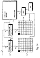
- the basic block diagram of the implementation of one embodiment of the present invention is shown in figure 14.
- the block diagram shows the case with two switch arrays 1a and 1b.
- the calibration algorithm and the mapper data has been saved in the calibration device 3.
- the calibration algorithm itself can be fully implemented with software.
- the calibration device 3 is connected to the programmable mapping devices 2a, 2b which are further connected to the switch arrays 1a, 1b.
- the I ref is a reference current source which is used for current comparison of the current sources in the arrays 1a and 1b.
- the reference current is mirrored from the same bias that is used for biasing the current sources of the DAC.
- the reference current can be designed for high precision performance by using averaging and common centroid layout, because there is no need for high speed operation for the ADC.
- the ADC is a low speed, low resolution ADC that is used for analysing the deviation of the current source current from the reference current.
- a 4-bit resolution is used in the calculations shown in the examples above.
- the ADC measuring range can be tuneable, so that the measurement range can be fixed to get the necessary range by measuring all sources and checking if the codes on the edges are not used.
- the calibration algorithm gets the deviation values of the current sources one by one and using these values sorts the switching order properly.
- the mapping data is loaded to the mapping device 2a, 2b and the DAC is ready for normal operation.
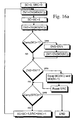
- the details of the calibration algorithm are explained in the following paragraphs with reference to figures 15 - 17.
- the hardware implementation of the algorithm is shown in figure 15. This also explains the required blocks mentioned in the software implementation.
- the resolution of the ADC determines the accuracy of the calibration method, and the resolution can be 2 - 6 bits. In these examples, a 4-bit resolution is used. If a higher resolution is used, the deviation value RAM increases also, since the word length determines the number of cells.
- the control logic controls the progress of the calibration.
- the calibration algorithm has four different phases. In the first phase the deviation data is collected with the ADC and stored in the deviation value RAM. The next two phases make the actual sorting. First, the data is sorted in increasing or decreasing order, and then the mapping device values are randomised, as shown in figures 7a and 7b. In the last phase, the correctly sorted mapping data is loaded to the mapping device.
- an initialise data is loaded to the mapping device from a ROM.
- This mapping data maps current sources from the array one by one so that all of the 63 current sources in each array can be separately measured. All of the currents are compared with the reference current, and the difference is converted with an ADC. In this example, a 4-bit ADC is used. Now for each of the current source there is a 4-bit number in the deviation value RAM that represents the deviation from the reference current.
- the sorting counter SC gives the address values for the Mapper Data MD, from where the addresses for the Deviation Value DV RAM are loaded.
- the Sorting Ready Counter SRC is a 6-bit counter that controls the progress of the sorting. When the SRC overflows and the carry bit is active, the first phase of the sorting is ready.
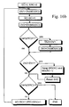
- the flowchart of the first phase of the calibration algorithm is shown in figures 16a - 16b in the case of the two switching arrays.
- the expression DV(MD(SC)) gives the value in the deviation value RAM DV pointed by the address value in the mapping data RAM MD.
- the address value from the mapping data RAM MD is sorting counter SC.
- DV1 and DV2 are the numbers from the deviation value RAM DV to be compared.
- a special case is when the SC counter overflows after reading the deviation value for DV1.
- the DV2 is loaded from the first address location. The last and the first value must be compared in reversed order. The carry signal of the SC counter is used for indicating the situation.”
- the comparison of the values DV1 and DV2 is done in reversed order.
- the values are in decreasing order, so that the first cell is the largest positive error and the last cell is the largest negative error.
- the same hardware implementation can be used.
- the deviation values can be discarded.
- the second phase of the calibration algorithm simply organises the mapping data into the final order.
- the second phase of the calibration algorithm takes numbers from the second half of the mapper data RAM and moves them to the first half of the mapper data RAM, so that the first memory location stays unchanged, the second is swapped with the last value.
- the third is unchanged, the fourth is swapped with the third from the end, etc.
- the flowchart of the algorithm is shown in figure 18.
- the term 'max' indicates the maximum value, 62 in this example, of SC counter. The flowchart is valid for both of the arrays if the two array structure is in use.
- the final phase the sorted mapping device is loaded to the mapping device. In the two array topology, all four phases are repeated with the second array.
Landscapes
- Engineering & Computer Science (AREA)
- Theoretical Computer Science (AREA)
- Physics & Mathematics (AREA)
- Nonlinear Science (AREA)
- Analogue/Digital Conversion (AREA)
Claims (16)
- Convertisseur numérique-analogique (CNA) comprenant :un ensemble de sources de courant commutables (1) configurées pour fonctionner dans un ordre prédéterminé ;caractérisé en ce que le convertisseur numérique-analogique (CNA) comprend en outre :un convertisseur analogique-numérique (CAN) configuré pour mesurer les données de déviation de courant proportionnellement à un courant de référence (Iref) provenant dudit ensemble de sources de courant commutables (1) ;un dispositif d'étalonnage (3) configuré pour étalonner le convertisseur numérique-analogique (CNA), lequel dispositif d'étalonnage (3) comprend en outre :un dispositif de tri configuré pour trier les sources de courant commutables (1) dans un ordre de commutation dans lequel les déviations positive et négative des sources de courant commutables (1) par rapport audit courant de référence (Iref) se compensent les unes les autres, et le convertisseur numérique-analogique (CNA) comprend en outre :un dispositif de mise en correspondance (2) connecté au dispositif d'étalonnage (3), lequel dispositif de mise en correspondance (2) est configuré pour commuter les sources de courant commutables (1) dans l'ordre de commutation trié chargé à partir du dispositif de tri.
- Convertisseur numérique-analogique (CNA) selon la revendication 1, caractérisé en ce que ledit convertisseur numérique-analogique (CNA) comprend en outre :le dispositif de tri configuré pour sélectionner l'ordre de commutation de sorte que la déviation positive la plus grande par rapport au courant de référence soit la première, que la déviation négative la plus grande par rapport au courant de référence soit la deuxième, que la troisième déviation positive la plus grande par rapport au courant de référence soit la troisième, que la troisième déviation négative la plus grande par rapport au courant de référence soit la quatrième, etc., dans lequel l'avant-dernière est la deuxième déviation négative la plus grande, et la dernière est la deuxième déviation positive la plus grande.
- Convertisseur numérique-analogique (CNA) selon la revendication 1, caractérisé en ce que ledit dispositif d'étalonnage (3) est configuré pour initialiser l'étalonnage en chargeant dans ledit dispositif de mise en correspondance (2) un élément de données de mise en correspondance qui commute lesdites sources de courant commutables (1) une à une en les comparant indépendamment au courant de référence (Iref).
- Convertisseur numérique-analogique (CNA) selon la revendication 1, caractérisé en ce que :ledit ensemble de sources de courant commutables (1) est divisé en deux matrices de sources de courant commutables (1a, 1b) ;ledit dispositif de mise en correspondance (2) est divisé en deux dispositifs de mise en correspondance indépendants (2a, 2b) qui sont connectés auxdites matrices de sources de courant commutables (1a, 1b) ; etledit dispositif de tri est configuré pour trier un premier élément de données de mise en correspondance pour la première matrice dans le premier ordre et un deuxième élément de données de mise en correspondance pour la seconde matrice dans l'ordre inverse par rapport au premier ordre.
- Convertisseur numérique-analogique (CNA) selon la revendication 1, caractérisé en ce que ledit dispositif d'étalonnage (3) comprend :un dispositif de stockage (RAM) configuré pour stocker ladite déviation de courant et/ou les données de mise en correspondance ; etune logique de commande pour commander ledit dispositif de tri.
- Convertisseur numérique-analogique (CNA) selon la revendication 1, caractérisé en ce que ledit dispositif de tri comprend :un compteur de tri (SC) configuré pour sauvegarder les valeurs d'adresse des données de déviation pour le dispositif de mise en correspondance (2) ; etun compteur prêt pour le tri (SRC) configuré pour commander la progression du tri.
- Convertisseur numérique-analogique (CNA) selon la revendication 1, caractérisé en ce que ledit dispositif de tri comprend :une mémoire morte (ROM) configurée pour stocker les données de mise en correspondance pour l'initialisation dudit dispositif d'étalonnage (3).
- Procédé d'étalonnage pour étalonner un convertisseur numérique-analogique, qui utilise un ensemble de sources de courant commutables, dans lequel procédé lesdites sources de courant commutables sont agencées pour fonctionner dans un ordre prédéterminé, caractérisé par
la mesure desdites données de déviation de courant par rapport à un courant de référence provenant dudit ensemble de sources de courant commutables avec un convertisseur analogique-numérique ;
le tri desdites sources de courant commutables dans un ordre de commutation dans lequel les déviations positive et négative des sources de courant commutables par rapport audit courant de référence se compensent les unes les autres ; et
le chargement dudit ordre de commutation dans un dispositif de mise en correspondance en tant que données de mise en correspondance pour commuter les sources de courant commutables dans l'ordre de commutation trié. - Procédé selon la revendication 8, caractérisé en ce que ladite étape de tri comprend :la sélection de l'ordre de commutation de sorte que la déviation positive la plus grande par rapport au courant de référence soit la première, la déviation négative la plus grande par rapport au courant de référence soit la deuxième, la troisième déviation positive la plus grande par rapport au courant de référence soit la troisième, la troisième déviation négative la plus grande par rapport au courant de référence soit la quatrième, etc., dans lequel l'avant dernière est la deuxième déviation négative la plus grande, et la dernière est la deuxième déviation positive la plus grande.
- Procédé selon la revendication 8, caractérisé par l'initialisation de l'étalonnage par le chargement dans ledit dispositif de mise en correspondance des données de mise en correspondance qui commute lesdites sources de courant commutables une à une en les comparant indépendamment au courant de référence.
- Procédé selon la revendication 8, caractérisé en ce que dans le cas de deux matrices indépendantes de sources de courant commutables, le tri d'un premier élément de données de mise en correspondance pour la première matrice dans le premier ordre et d'un second élément de données de mise en correspondance pour la seconde matrice dans l'ordre inverse par rapport au premier ordre.
- Procédé selon la revendication 8, caractérisé en ce que le procédé comprend en outre :le stockage de ladite déviation de courant et/ou des données de mise en correspondance dans un dispositif de stockage ; etla commande dudit dispositif de tri par la logique de commande.
- Procédé selon la revendication 8, caractérisé en ce que le procédé comprend en outre :la sauvegarde des valeurs d'adresse des données de déviation pour la procédure de mise en correspondance dans un compteur de tri ; etla commande de la progression du tri dans un compteur prêt pour le tri.
- Procédé selon la revendication 8, caractérisé en ce que le procédé comprend en outre :le stockage des données de mise en correspondance pour l'initialisation dudit dispositif d'étalonnage dans une mémoire morte.
- Un circuit intégré, caractérisé en ce qu'il comprend un convertisseur numérique-analogique décrit dans l'une quelconque des revendications 1 à 7.
- Un programme d'ordinateur pour calibrer un convertisseur numérique-analogique, caractérisé en ce que le programme d'ordinateur comprend un code adapté à opérer les étapes de procédé décrites dans l'une quelconque des étapes de procédé 8 à 14.
Priority Applications (1)
| Application Number | Priority Date | Filing Date | Title |
|---|---|---|---|
| AT02724361T ATE343250T1 (de) | 2002-05-27 | 2002-05-27 | Verfahren zum kalibrieren eines digital/analog- umsetzers und digital/analog-umsetzer |
Applications Claiming Priority (1)
| Application Number | Priority Date | Filing Date | Title |
|---|---|---|---|
| PCT/FI2002/000454 WO2003100982A1 (fr) | 2002-05-27 | 2002-05-27 | Procede d'etalonnage d'un convertisseur numerique-analogique et convertisseur numerique-analogique |
Publications (2)
| Publication Number | Publication Date |
|---|---|
| EP1510009A1 EP1510009A1 (fr) | 2005-03-02 |
| EP1510009B1 true EP1510009B1 (fr) | 2006-10-18 |
Family
ID=29558525
Family Applications (1)
| Application Number | Title | Priority Date | Filing Date |
|---|---|---|---|
| EP02724361A Expired - Lifetime EP1510009B1 (fr) | 2002-05-27 | 2002-05-27 | Procede d'etalonnage d'un convertisseur numerique-analogique et convertisseur numerique-analogique |
Country Status (7)
| Country | Link |
|---|---|
| US (2) | US7026967B2 (fr) |
| EP (1) | EP1510009B1 (fr) |
| KR (1) | KR100730398B1 (fr) |
| CN (1) | CN100481730C (fr) |
| AU (1) | AU2002255056A1 (fr) |
| DE (1) | DE60215560T2 (fr) |
| WO (1) | WO2003100982A1 (fr) |
Cited By (1)
| Publication number | Priority date | Publication date | Assignee | Title |
|---|---|---|---|---|
| US9362937B1 (en) | 2014-11-26 | 2016-06-07 | Stmicroelectronics S.R.L. | Method of calibrating a SAR A/D converter and SAR-A/D converter implementing said method |
Families Citing this family (42)
| Publication number | Priority date | Publication date | Assignee | Title |
|---|---|---|---|---|
| US6885323B2 (en) * | 2003-06-27 | 2005-04-26 | Optichron, Inc. | Analog to digital converter with distortion correction |
| KR100631872B1 (ko) * | 2004-03-31 | 2006-10-04 | 윤홍일 | 아날로그-디지털 변환기의 비아이에스티 및 비아이에스씨장치 |
| US7394414B2 (en) * | 2004-04-20 | 2008-07-01 | Nxp B.V. | Error reduction in a digital-to-analog (DAC) converter |
| TWI254512B (en) | 2005-03-08 | 2006-05-01 | Sunplus Technology Co Ltd | Apparatus, method and digital-to-analog converter for reducing harmonic error power |
| CN101180799B (zh) * | 2005-05-20 | 2012-01-18 | 松下电器产业株式会社 | D/a转换器和具有它的半导体集成电路 |
| JP4757006B2 (ja) * | 2005-12-07 | 2011-08-24 | ルネサスエレクトロニクス株式会社 | 電流源セル配置構造およびda変換器 |
| GB2453298B (en) * | 2006-06-28 | 2011-04-06 | Analog Devices Inc | Return-to-hold switching scheme for DAC output stage |
| JP4836736B2 (ja) * | 2006-09-29 | 2011-12-14 | 株式会社東芝 | デジタル・アナログ変換回路 |
| US7557743B2 (en) * | 2006-12-08 | 2009-07-07 | Kabushiki Kaisha Toshiba | D/A converter |
| US7633415B2 (en) * | 2007-03-27 | 2009-12-15 | Taiwan Semiconductor Manufacturing Co., Ltd. | System and method for calibrating digital-to-analog convertors |
| CN100592635C (zh) * | 2007-04-25 | 2010-02-24 | 中国科学院微电子研究所 | 一种运放共享的乘法数字模拟转换电路及应用 |
| CN101237238B (zh) * | 2007-12-29 | 2011-05-18 | 湖南大学 | 基于开关电流技术的cmos电流舵da转换器 |
| CN101686057B (zh) * | 2008-09-28 | 2012-02-29 | 扬智科技股份有限公司 | 数字模拟转换器 |
| US8422588B2 (en) * | 2009-04-01 | 2013-04-16 | Intel Mobile Communications GmbH | Variable-size mixer for high gain range transmitter |
| US7978110B2 (en) * | 2009-05-11 | 2011-07-12 | Taiwan Semiconductor Manufacturing Company, Ltd. | Digital-to-analog converter |
| US8456342B2 (en) * | 2011-05-03 | 2013-06-04 | Microchip Technology Incorporated | Switch sequencing for code-range-specific linearity improvement in digital-to-analog converters |
| CN102522988B (zh) * | 2011-12-30 | 2014-06-04 | 清华大学 | 对称电流源阵列的开关序列的生成方法、装置及其应用 |
| CN102769470B (zh) * | 2012-07-26 | 2014-12-10 | 浙江大学 | 一种具有时域误差校正功能的电流舵数模转换器 |
| TWI558106B (zh) * | 2012-10-29 | 2016-11-11 | 聯華電子股份有限公司 | 數位類比轉換器 |
| US8981981B1 (en) * | 2013-03-15 | 2015-03-17 | Google Inc. | Digital-to-analog converter with monotonicity |
| CN103412202B (zh) * | 2013-06-08 | 2016-08-17 | 惠州市亿能电子有限公司 | 一种电流分区间校准的方法 |
| US8779953B1 (en) * | 2013-07-31 | 2014-07-15 | Google Inc. | Fast test of digital-to-analog converters |
| US9094042B2 (en) * | 2013-08-09 | 2015-07-28 | Silicon Laboratories Inc. | DAC current source matrix patterns with gradient error cancellation |
| US9432041B2 (en) * | 2014-04-17 | 2016-08-30 | Stmicroelectronics S.R.L. | Method of calibrating a thermometer-code SAR A/D converter and thermometer-code SAR-A/D converter implementing said method |
| US9124287B1 (en) * | 2014-12-22 | 2015-09-01 | Pmc-Sierra Us, Inc. | Scrambler with built in test capabilities for unary DAC |
| US9853654B2 (en) * | 2015-02-25 | 2017-12-26 | Qualcomm Incorporated | Error-feedback digital-to-analog converter (DAC) |
| US10296612B2 (en) | 2015-09-29 | 2019-05-21 | At&T Mobility Ii Llc | Sorting system |
| US10416959B2 (en) * | 2015-10-27 | 2019-09-17 | At&T Mobility Ii Llc | Analog sorter |
| US10261832B2 (en) | 2015-12-02 | 2019-04-16 | At&T Mobility Ii Llc | Sorting apparatus |
| US9438266B1 (en) * | 2016-02-10 | 2016-09-06 | Texas Instruments Incorporated | Calibrated-output analog-to-digital converter apparatus and methods |
| US9654131B1 (en) * | 2016-02-26 | 2017-05-16 | Texas Instruments Deutschland Gmbh | Capacitor order determination in an analog-to-digital converter |
| CN106487384A (zh) * | 2016-10-11 | 2017-03-08 | 上海华虹集成电路有限责任公司 | 用于数模转换电路的自校准电路 |
| CN106656181B (zh) * | 2016-11-16 | 2023-05-16 | 杰华特微电子股份有限公司 | 一种数模转换器的控制方法及数模转换器 |
| US10298257B1 (en) * | 2018-12-17 | 2019-05-21 | Nxp Usa, Inc. | SNDR improvement through optimal DAC element selection |
| CN110855295B (zh) * | 2019-11-06 | 2023-06-13 | 珠海亿智电子科技有限公司 | 一种数模转换器和控制方法 |
| KR102738188B1 (ko) * | 2019-11-11 | 2024-12-05 | 삼성전자주식회사 | 디지털-아날로그 컨버터 및 이를 포함하는 전자 시스템 |
| CN115398808A (zh) * | 2020-04-20 | 2022-11-25 | 华为技术有限公司 | 减少由失配导致的数模转换器噪声的技术 |
| CN114553226A (zh) * | 2020-11-25 | 2022-05-27 | 杭州深谙微电子科技有限公司 | 模数转换器的校准方法和校准系统 |
| CN112865793B (zh) * | 2021-01-15 | 2024-09-27 | 成都环宇芯科技有限公司 | 数模转换器的校准转换方法 |
| TWI768973B (zh) * | 2021-06-17 | 2022-06-21 | 瑞昱半導體股份有限公司 | 校正輸出電流的方法、電流控制系統及電壓控制系統 |
| TWI812975B (zh) * | 2021-07-13 | 2023-08-21 | 瑞昱半導體股份有限公司 | 具有訊號校正機制的數位至類比轉換電路及方法 |
| CN116155285B (zh) * | 2023-03-27 | 2026-02-24 | 昇陌微电子(苏州)有限公司 | 一种基于数字域编码重映射的数模转换器校准方法 |
Family Cites Families (13)
| Publication number | Priority date | Publication date | Assignee | Title |
|---|---|---|---|---|
| US5995980A (en) * | 1996-07-23 | 1999-11-30 | Olson; Jack E. | System and method for database update replication |
| US5949362A (en) * | 1997-08-22 | 1999-09-07 | Harris Corporation | Digital-to-analog converter including current cell matrix with enhanced linearity and associated methods |
| US5955980A (en) * | 1997-10-03 | 1999-09-21 | Motorola, Inc. | Circuit and method for calibrating a digital-to-analog converter |
| GB2368209B (en) | 1998-01-08 | 2002-06-12 | Fujitsu Ltd | Cell array circuitry |
| WO2000057558A2 (fr) * | 1999-03-22 | 2000-09-28 | Siemens Aktiengesellschaft | Circuit convertisseur numerique-analogique 1 bit |
| KR100592220B1 (ko) * | 1999-04-23 | 2006-06-23 | 삼성전자주식회사 | 디지털/아날로그 컨버터 및 그를 이용한 액정표시장치의 소스 구동 회로 |
| KR20000072961A (ko) * | 1999-05-03 | 2000-12-05 | 윤종용 | 전류 세그먼트형 디지털-아날로그 변환기 |
| CN1152471C (zh) * | 2000-01-17 | 2004-06-02 | 华为技术有限公司 | I2c逻辑的电流舵结构数模转换器 |
| JP3528958B2 (ja) * | 2000-06-28 | 2004-05-24 | 松下電器産業株式会社 | 電流加算型da変換器 |
| GB0111313D0 (en) * | 2001-05-09 | 2001-07-04 | Broadcom Corp | Digital-to-analogue converter using an array of current sources |
| US6507304B1 (en) * | 2002-05-02 | 2003-01-14 | National Semiconductor Corporation | Current steering segmented DAC system |
| JP3843942B2 (ja) * | 2002-12-25 | 2006-11-08 | 株式会社デンソー | D/a変換器およびa/d変換器 |
| US6720898B1 (en) * | 2003-04-10 | 2004-04-13 | Maxim Integrated Products, Inc. | Current source array for high speed, high resolution current steering DACs |
-
2002
- 2002-05-27 EP EP02724361A patent/EP1510009B1/fr not_active Expired - Lifetime
- 2002-05-27 AU AU2002255056A patent/AU2002255056A1/en not_active Abandoned
- 2002-05-27 CN CNB028288157A patent/CN100481730C/zh not_active Expired - Fee Related
- 2002-05-27 DE DE60215560T patent/DE60215560T2/de not_active Expired - Lifetime
- 2002-05-27 WO PCT/FI2002/000454 patent/WO2003100982A1/fr not_active Ceased
- 2002-05-27 KR KR1020047018235A patent/KR100730398B1/ko not_active Expired - Fee Related
-
2004
- 2004-10-22 US US10/970,393 patent/US7026967B2/en not_active Expired - Lifetime
-
2006
- 2006-01-05 US US11/325,449 patent/US20060114138A1/en not_active Abandoned
Cited By (1)
| Publication number | Priority date | Publication date | Assignee | Title |
|---|---|---|---|---|
| US9362937B1 (en) | 2014-11-26 | 2016-06-07 | Stmicroelectronics S.R.L. | Method of calibrating a SAR A/D converter and SAR-A/D converter implementing said method |
Also Published As
| Publication number | Publication date |
|---|---|
| US7026967B2 (en) | 2006-04-11 |
| US20050052297A1 (en) | 2005-03-10 |
| CN1625840A (zh) | 2005-06-08 |
| DE60215560T2 (de) | 2007-06-21 |
| WO2003100982A1 (fr) | 2003-12-04 |
| US20060114138A1 (en) | 2006-06-01 |
| KR100730398B1 (ko) | 2007-06-20 |
| CN100481730C (zh) | 2009-04-22 |
| AU2002255056A1 (en) | 2003-12-12 |
| EP1510009A1 (fr) | 2005-03-02 |
| KR20050003442A (ko) | 2005-01-10 |
| DE60215560D1 (de) | 2006-11-30 |
Similar Documents
| Publication | Publication Date | Title |
|---|---|---|
| EP1510009B1 (fr) | Procede d'etalonnage d'un convertisseur numerique-analogique et convertisseur numerique-analogique | |
| EP0898374B1 (fr) | Convertisseur numérique-analogique comprenant une matrice de sources de courant à linéarité améliorée et procédés associés | |
| US7068201B1 (en) | Digital-to-analog converter | |
| US5703586A (en) | Digital-to-analog converter having programmable transfer function errors and method of programming same | |
| CN104604142B (zh) | 减少sar adc中的元件失配的影响 | |
| US10097198B1 (en) | Sar adc | |
| US8947290B2 (en) | Successive approximation AD converter | |
| EP1792402B1 (fr) | Structures de convertisseur numerique-analogique | |
| EP3624345B1 (fr) | Modification de fonction de transfert convertisseur numérique-analogique | |
| US6118398A (en) | Digital-to-analog converter including current sources operable in a predetermined sequence and associated methods | |
| US20160149583A1 (en) | Method of calibrating a sar a/d converter and sar-a/d converter implementing said method | |
| KR20060135074A (ko) | 디지털-아날로그 변환기에서의 에러 감소율 개선 방법 및디지털-아날로그 변환기 | |
| Kvashina et al. | Comparative analysis of switching-based calibration algorithms for DACs | |
| US7173552B1 (en) | High accuracy segmented DAC | |
| Amankrah et al. | A Strategic Approach to Enhancing INL Performance in 10-Bit MOS-Based R-2R DACs through Area Allocation | |
| US8253612B2 (en) | Self-calibrating R-2R ladder and method thereof | |
| Zeng et al. | New calibration technique for current-steering DACs | |
| KR100546412B1 (ko) | 디지털-아날로그 변환기와 디지털-아날로그 변환 방법 | |
| Parthasarathy et al. | A 16-bit resistor string DAC with full-calibration at final test | |
| US6879276B2 (en) | Split cell bowtie digital to analog converter and method | |
| CN115940949B (zh) | 分裂电容结构逐次逼近模数转换器校准电路及方法 | |
| US5631649A (en) | Digital-to-analog converter test method and apparatus | |
| Valet et al. | Comparative study on pre-distortion/calibration methods for current-steering digital-to-analog converters | |
| US6469646B1 (en) | Converting digital signals to analog signals | |
| Koh et al. | An 8 bit to 12 bit resolution programmable 5 msample/s current steering digital-to-analog converter in a 22 nm fd-soi cmos technology |
Legal Events
| Date | Code | Title | Description |
|---|---|---|---|
| PUAI | Public reference made under article 153(3) epc to a published international application that has entered the european phase |
Free format text: ORIGINAL CODE: 0009012 |
|
| 17P | Request for examination filed |
Effective date: 20040915 |
|
| AK | Designated contracting states |
Kind code of ref document: A1 Designated state(s): AT BE CH CY DE DK ES FI FR GB GR IE IT LI LU MC NL PT SE TR |
|
| AX | Request for extension of the european patent |
Extension state: AL LT LV MK RO SI |
|
| 17Q | First examination report despatched |
Effective date: 20050614 |
|
| DAX | Request for extension of the european patent (deleted) | ||
| GRAP | Despatch of communication of intention to grant a patent |
Free format text: ORIGINAL CODE: EPIDOSNIGR1 |
|
| GRAS | Grant fee paid |
Free format text: ORIGINAL CODE: EPIDOSNIGR3 |
|
| GRAA | (expected) grant |
Free format text: ORIGINAL CODE: 0009210 |
|
| AK | Designated contracting states |
Kind code of ref document: B1 Designated state(s): AT BE CH CY DE DK ES FI FR GB GR IE IT LI LU MC NL PT SE TR |
|
| PG25 | Lapsed in a contracting state [announced via postgrant information from national office to epo] |
Ref country code: IT Free format text: LAPSE BECAUSE OF FAILURE TO SUBMIT A TRANSLATION OF THE DESCRIPTION OR TO PAY THE FEE WITHIN THE PRESCRIBED TIME-LIMIT;WARNING: LAPSES OF ITALIAN PATENTS WITH EFFECTIVE DATE BEFORE 2007 MAY HAVE OCCURRED AT ANY TIME BEFORE 2007. THE CORRECT EFFECTIVE DATE MAY BE DIFFERENT FROM THE ONE RECORDED. Effective date: 20061018 Ref country code: LI Free format text: LAPSE BECAUSE OF FAILURE TO SUBMIT A TRANSLATION OF THE DESCRIPTION OR TO PAY THE FEE WITHIN THE PRESCRIBED TIME-LIMIT Effective date: 20061018 Ref country code: AT Free format text: LAPSE BECAUSE OF FAILURE TO SUBMIT A TRANSLATION OF THE DESCRIPTION OR TO PAY THE FEE WITHIN THE PRESCRIBED TIME-LIMIT Effective date: 20061018 Ref country code: BE Free format text: LAPSE BECAUSE OF FAILURE TO SUBMIT A TRANSLATION OF THE DESCRIPTION OR TO PAY THE FEE WITHIN THE PRESCRIBED TIME-LIMIT Effective date: 20061018 Ref country code: CH Free format text: LAPSE BECAUSE OF FAILURE TO SUBMIT A TRANSLATION OF THE DESCRIPTION OR TO PAY THE FEE WITHIN THE PRESCRIBED TIME-LIMIT Effective date: 20061018 |
|
| REG | Reference to a national code |
Ref country code: GB Ref legal event code: FG4D |
|
| REG | Reference to a national code |
Ref country code: IE Ref legal event code: FG4D Ref country code: CH Ref legal event code: EP |
|
| REF | Corresponds to: |
Ref document number: 60215560 Country of ref document: DE Date of ref document: 20061130 Kind code of ref document: P |
|
| PG25 | Lapsed in a contracting state [announced via postgrant information from national office to epo] |
Ref country code: SE Free format text: LAPSE BECAUSE OF FAILURE TO SUBMIT A TRANSLATION OF THE DESCRIPTION OR TO PAY THE FEE WITHIN THE PRESCRIBED TIME-LIMIT Effective date: 20070118 Ref country code: DK Free format text: LAPSE BECAUSE OF FAILURE TO SUBMIT A TRANSLATION OF THE DESCRIPTION OR TO PAY THE FEE WITHIN THE PRESCRIBED TIME-LIMIT Effective date: 20070118 |
|
| PG25 | Lapsed in a contracting state [announced via postgrant information from national office to epo] |
Ref country code: ES Free format text: LAPSE BECAUSE OF FAILURE TO SUBMIT A TRANSLATION OF THE DESCRIPTION OR TO PAY THE FEE WITHIN THE PRESCRIBED TIME-LIMIT Effective date: 20070129 |
|
| PG25 | Lapsed in a contracting state [announced via postgrant information from national office to epo] |
Ref country code: PT Free format text: LAPSE BECAUSE OF FAILURE TO SUBMIT A TRANSLATION OF THE DESCRIPTION OR TO PAY THE FEE WITHIN THE PRESCRIBED TIME-LIMIT Effective date: 20070319 |
|
| ET | Fr: translation filed | ||
| REG | Reference to a national code |
Ref country code: CH Ref legal event code: PL |
|
| PLBE | No opposition filed within time limit |
Free format text: ORIGINAL CODE: 0009261 |
|
| STAA | Information on the status of an ep patent application or granted ep patent |
Free format text: STATUS: NO OPPOSITION FILED WITHIN TIME LIMIT |
|
| 26N | No opposition filed |
Effective date: 20070719 |
|
| PG25 | Lapsed in a contracting state [announced via postgrant information from national office to epo] |
Ref country code: MC Free format text: LAPSE BECAUSE OF NON-PAYMENT OF DUE FEES Effective date: 20070531 |
|
| PG25 | Lapsed in a contracting state [announced via postgrant information from national office to epo] |
Ref country code: GR Free format text: LAPSE BECAUSE OF FAILURE TO SUBMIT A TRANSLATION OF THE DESCRIPTION OR TO PAY THE FEE WITHIN THE PRESCRIBED TIME-LIMIT Effective date: 20070119 |
|
| PG25 | Lapsed in a contracting state [announced via postgrant information from national office to epo] |
Ref country code: IE Free format text: LAPSE BECAUSE OF NON-PAYMENT OF DUE FEES Effective date: 20070528 |
|
| PG25 | Lapsed in a contracting state [announced via postgrant information from national office to epo] |
Ref country code: LU Free format text: LAPSE BECAUSE OF NON-PAYMENT OF DUE FEES Effective date: 20070527 Ref country code: CY Free format text: LAPSE BECAUSE OF FAILURE TO SUBMIT A TRANSLATION OF THE DESCRIPTION OR TO PAY THE FEE WITHIN THE PRESCRIBED TIME-LIMIT Effective date: 20061018 |
|
| PG25 | Lapsed in a contracting state [announced via postgrant information from national office to epo] |
Ref country code: TR Free format text: LAPSE BECAUSE OF FAILURE TO SUBMIT A TRANSLATION OF THE DESCRIPTION OR TO PAY THE FEE WITHIN THE PRESCRIBED TIME-LIMIT Effective date: 20061018 |
|
| PGFP | Annual fee paid to national office [announced via postgrant information from national office to epo] |
Ref country code: FI Payment date: 20100512 Year of fee payment: 9 Ref country code: FR Payment date: 20100525 Year of fee payment: 9 |
|
| PGFP | Annual fee paid to national office [announced via postgrant information from national office to epo] |
Ref country code: NL Payment date: 20100501 Year of fee payment: 9 |
|
| PGFP | Annual fee paid to national office [announced via postgrant information from national office to epo] |
Ref country code: GB Payment date: 20110525 Year of fee payment: 10 |
|
| REG | Reference to a national code |
Ref country code: NL Ref legal event code: V1 Effective date: 20111201 |
|
| PG25 | Lapsed in a contracting state [announced via postgrant information from national office to epo] |
Ref country code: FI Free format text: LAPSE BECAUSE OF NON-PAYMENT OF DUE FEES Effective date: 20110527 Ref country code: NL Free format text: LAPSE BECAUSE OF NON-PAYMENT OF DUE FEES Effective date: 20111201 |
|
| REG | Reference to a national code |
Ref country code: FR Ref legal event code: ST Effective date: 20120131 |
|
| PG25 | Lapsed in a contracting state [announced via postgrant information from national office to epo] |
Ref country code: FR Free format text: LAPSE BECAUSE OF NON-PAYMENT OF DUE FEES Effective date: 20110531 |
|
| GBPC | Gb: european patent ceased through non-payment of renewal fee |
Effective date: 20120527 |
|
| PG25 | Lapsed in a contracting state [announced via postgrant information from national office to epo] |
Ref country code: GB Free format text: LAPSE BECAUSE OF NON-PAYMENT OF DUE FEES Effective date: 20120527 |
|
| REG | Reference to a national code |
Ref country code: DE Ref legal event code: R082 Ref document number: 60215560 Country of ref document: DE Representative=s name: COHAUSZ & FLORACK PATENT- UND RECHTSANWAELTE P, DE Ref country code: DE Ref legal event code: R081 Ref document number: 60215560 Country of ref document: DE Owner name: NOKIA TECHNOLOGIES OY, FI Free format text: FORMER OWNER: NOKIA CORP., 02610 ESPOO, FI |
|
| REG | Reference to a national code |
Ref country code: DE Ref legal event code: R082 Ref document number: 60215560 Country of ref document: DE Representative=s name: WINTER, BRANDL - PARTNERSCHAFT MBB, PATENTANWA, DE Ref country code: DE Ref legal event code: R081 Ref document number: 60215560 Country of ref document: DE Owner name: VIVO MOBILE COMMUNICATION CO., LTD., DONGGUAN, CN Free format text: FORMER OWNER: NOKIA TECHNOLOGIES OY, ESPOO, FI |
|
| PGFP | Annual fee paid to national office [announced via postgrant information from national office to epo] |
Ref country code: DE Payment date: 20210511 Year of fee payment: 20 |
|
| REG | Reference to a national code |
Ref country code: DE Ref legal event code: R071 Ref document number: 60215560 Country of ref document: DE |