EP1511087A2 - Procédé de dépot de particules sur une surface de substrate et cellules solaires avec des couches fonctionelles - Google Patents
Procédé de dépot de particules sur une surface de substrate et cellules solaires avec des couches fonctionelles Download PDFInfo
- Publication number
- EP1511087A2 EP1511087A2 EP04090308A EP04090308A EP1511087A2 EP 1511087 A2 EP1511087 A2 EP 1511087A2 EP 04090308 A EP04090308 A EP 04090308A EP 04090308 A EP04090308 A EP 04090308A EP 1511087 A2 EP1511087 A2 EP 1511087A2
- Authority
- EP
- European Patent Office
- Prior art keywords
- particles
- coating method
- chalcogenide
- particle
- substrate surface
- Prior art date
- Legal status (The legal status is an assumption and is not a legal conclusion. Google has not performed a legal analysis and makes no representation as to the accuracy of the status listed.)
- Withdrawn
Links
Images

Classifications
-
- H—ELECTRICITY
- H10—SEMICONDUCTOR DEVICES; ELECTRIC SOLID-STATE DEVICES NOT OTHERWISE PROVIDED FOR
- H10F—INORGANIC SEMICONDUCTOR DEVICES SENSITIVE TO INFRARED RADIATION, LIGHT, ELECTROMAGNETIC RADIATION OF SHORTER WAVELENGTH OR CORPUSCULAR RADIATION
- H10F71/00—Manufacture or treatment of devices covered by this subclass
- H10F71/125—The active layers comprising only Group II-VI materials, e.g. CdS, ZnS or CdTe
-
- Y—GENERAL TAGGING OF NEW TECHNOLOGICAL DEVELOPMENTS; GENERAL TAGGING OF CROSS-SECTIONAL TECHNOLOGIES SPANNING OVER SEVERAL SECTIONS OF THE IPC; TECHNICAL SUBJECTS COVERED BY FORMER USPC CROSS-REFERENCE ART COLLECTIONS [XRACs] AND DIGESTS
- Y02—TECHNOLOGIES OR APPLICATIONS FOR MITIGATION OR ADAPTATION AGAINST CLIMATE CHANGE
- Y02E—REDUCTION OF GREENHOUSE GAS [GHG] EMISSIONS, RELATED TO ENERGY GENERATION, TRANSMISSION OR DISTRIBUTION
- Y02E10/00—Energy generation through renewable energy sources
- Y02E10/50—Photovoltaic [PV] energy
- Y02E10/543—Solar cells from Group II-VI materials
Definitions
- the present invention relates to a coating method for Deposition and fixation of particles on a substrate surface and on Solar cells with functional layer structure.
- colloidal deposition is direct synthesis of the particles on a substrate surface via electrodeposition, chemical bath deposition, or pure adsorption of the particles, where the colloidal solution is simply applied to the substrate surface (see Publication I of S. Papp et al .: “Growth of Pd nanoparticles on layer silicates hydrophobized with alkyl chains in ethanol tetrahydrofuran mixtures "(Colloid Polym Sci (2002) 280: 956-962) and Publication II of H. Bönnemann et al .:” Nanoscopic Metal Particles - Synthetic Methods and Potential Applications "( Eur. J. Inorg. Chem. 2001, 2455-2480)).
- a disadvantage of these methods is that they each deposit only a monolayer of particles on the substrate surface.
- the adhesion of the material is problematic in the case of simple adsorption. This is especially true when the applied particles have to be modified by an annealing step, which is relatively often the case.
- the direct deposition of the particles on a substrate surface is to distinguish their incorporation into a matrix material with which the substrate is coated.
- the advantage of this embedding is the improved adhesion of the particles.
- additional functions can be fulfilled by the surface coating over the matrix material.
- the wet-chemical sol-gel process is often used, in which the particles are applied in a sol which solidifies on the substrate surface by evaporation to a gel and fixes the particles. Ultimately, the particles are thus embedded in an airgel (see Publication II).
- the sol-gel method fixes the particles in a matrix and thus prevents agglomeration during an annealing step, it has serious disadvantages.
- Highly porous materials, such as those used in catalysts are only superficially coated with the sol-gel process because the pores are capped. Thus, the inner walls of small pores remain uncoated.
- the variety of materials is significantly limited, since the process can not be performed with any components. Furthermore, only relatively thick layers can be applied.
- the destruction is for the substrate is not always guaranteed because of high process temperatures be driven, and a large-scale deposition leads to significant technological challenges.
- Cost-effective alternatives These are the already mentioned wet-chemical deposition methods.
- Here can be dispensed with vacuum and high process temperatures and In addition, no large amount of equipment is required.
- the wet chemical Coating (CBD) can take place in one or more process steps, leads however due to already small fluctuations in the process parameters (Temperature and pH) to agglomerates, which are located on the Substrate attach and the homogeneity and physical properties of the deposited film.
- the thickness of the Coating which about the concentration and the molar ratio the starting substances and over the deposition time is set, is strongly influenced by fluctuations.
- a compound is deposited on the substrate containing the cation of the desired end product.
- this is a metal salt.
- these salts are dissolved in a solvent. By immersing and pulling out the substrate from the solution (dip method) or by spraying the solution, the metal salt is applied to the substrate surface.
- the metal salt film dries in an inert gas stream (not applicable to smooth, non-porous substrates).
- the starting salt is gassed with a reactant gas yielding the anion of the final product and converted to the desired end product, the metal chalcogenide. It is therefore a chemical reaction between a solid and a gas.
- the ILGAR process is also a sequential process, allowing full material utilization but completely avoiding the formation of agglomerates.
- the layer thickness is set by the number of repetitions of the process steps. Since the educt supplying the anion is gaseous, the reaction itself still takes place in strongly narrowed pores.
- ILGAR process thus also offers the possibility of directly influencing the optical and electrical properties of the deposited thin films.
- the only condition for the reaction product is that it must be insoluble in the starting solution due to the cyclical nature of the manufacturing process. Since this is the case with a suitable choice of the solvent for many compounds, opens up a wide range of applications.
- the ILGAR procedure is now well established and extensively described in the art.
- the coating method according to the invention is a fixation of Particles with the ILGAR method on a substrate surface arbitrary Morphology made.
- all the benefits of the ILGAR process can be transferred to the coating process of the invention.
- the particles are embedded in the material via their embedding the chalcogenide matrix safely adhere to the substrate surface, homogeneous distributed and prevented from agglomerating. Because the particles neither in the coating process itself are still generated at a chemical Reaction involved can be particles of different materials and Sizes can be used in pure or mixed form. Important in the Use of the particles is that they are in the starting solution used are insoluble and distributed homogeneously in this and not at the bottom of the Deposit storage container.
- Particle diameter of several microns up to a few nanometers are possible, it can be monodisperse (only one particle diameter) or multidisperse mixtures used become.
- the particles used may be metal particles and particles of insoluble inorganic, but also organic Act connections. Their production is known, some of which are Particles in the form of colloidal suspensions commercially available. It is particularly advantageous in the coating method according to the invention So by the largely free choice of the materials involved (both the Chalcogenide matrix as well as the particles) the exact adjustability of the physical and chemical properties of the coating produced. This allows these very different functional properties have (see below).
- the coating process according to the Invention in addition to large-scale application areas in the Nanotechnology find its application.
- the chalcogenide matrix is used in the coating process according to the invention provided through the ILGAR process. Particles whose size is up to can range in microns, and chalcogenide matrix become simultaneous deposited. This is guaranteed by adding to the starting solution of the ILGAR process the particles as powder or in colloidal preparation be added, so that there is a particle-containing solution. at Use of particles with a size in the nanometer range arises according to a colloidal solution.
- the solvent used is so chosen that it is the metal compound, as a rule, this is about a metal salt, but not the particles.
- the metal compound and the Particles within the solution mix well so it is guaranteed that in the step of applying the particulate solution to the Substrate surface, the deposited layer also from a homogeneous Mixture exists. A here possibly already beginning agglomeration The particle is prevented because the solvent evaporates quickly.
- the dry and solid precursor layer is then in the actual reaction step by gassing with a chalcogen-containing gas as reactant gas modified so that the outgoing metal compound, the starting salt, is chemically converted to the desired end product.
- the particles in a favorable case not in the reaction with the Reactant gas involved.
- the particles are in after the gassing step Homogeneous distribution fixed in the resulting chalcogenide matrix and can also no longer be followed by any subsequent rinsing steps or the next time the substrate is immersed in the particulate starting solution dissolve out of this. Also required annealing steps, which at a Oxid matrix lead to drainage and generally to the growth of crystallites, do not lead to agglomeration of the particles.
- optically absorbing particles When using optically absorbing particles, however, all have the same diameter (monodisperse colloid), and the Use of a crystal structure of the matrix, which does not conform to the Is the crystal structure of the particle, the phonon-photon coupling in the suppressed layer can be suppressed. Therefore results in the absorption behavior the layer produced a sharp, steeply rising absorption edge.
- Optical filters provide a potential for such a layer
- multidisperse colloids may also be used optically fluorescent particles are used. Again, the Crystal structure of the matrix does not conform to the crystal structure of the colloid so that again a suppression of the phonon-photon coupling results. For fluorescent particles, this results in a narrow frequency range caused by the fluorescent light.
- such Layers are used to make optical absorption areas less favorable Compensate components. This is done by light of a photon energy greater than the absorption edge to be avoided via fluorescence in light smaller photon energy than this edge is converted.
- interesting These layers are used in solar cells. Here can be UV light in visible light to be converted, resulting in a higher conversion rate of light electric current leads. This generally applies to all solar cells. Particularly Let's take a look at the chalcopyrite thin-film solar cell. This one has a UV-absorbing window layer covering the wavelength range absorbed almost completely, so that it is no longer the actual Absorber layer comes. The result is a loss of power that has been in purchasing so far had to be taken (see also special description section).
- particle layers also show an anti-reflection effect, the occurring interference of the light radiation completely suppressed.
- Advantage of using in particular colloids as fluorescent Particles is thus the effected adjustment of their absorption and fluorescence range about the particle size (size quantization effect). Is possible Therefore, a multilayer system of particle layers with particles increasing Size. It can thereby be achieved that the fluorescence region the upper particle layer exactly the absorption area of the underlying Particle layer is. There is a fluorescence absorption cascade, until light is generated, which has an optimum of photocurrent in the Solar cell has the consequence. In organic this is for example at Plants with different sized chlorophyll instead.
- Magnetic and optical properties can also be used for particles Influencing other properties are used.
- plastic particles that are in a corresponding Polymer colloid can be used. These can be in any ILGAR layers be used, the melting point, however, above the used Plastic must lie. After completion of the coating process Then the plastic particles can be melted out, so that a correspondingly homogeneous, micro- to nanoporous thin coating is formed.
- Possible fields of application here are the production of filters and the Membrane technology.
- color pigments in a transparent Embedded ILGAR matrix to increase the scratch resistance of Coats of paint through the poorly soluble, ultra-hard ILGAR coating to reach.
- the addition of particulate in the ILGAR coating still an increase in surface strength and surface roughness be achieved.
- the addition of particles from the same material as the ILGAR matrix achieved faster growth of thicker ILGAR layers because the material-identical particles serve as growth nuclei.
- the coating process according to the invention is based on the known ILGAR process, with which easily, without a high process temperature, such as is required in the pyrolysis process to initiate a chemical reaction, thin, poorly soluble chalcogenidic, oxidic, ceramic and metallic layers on substrates with arbitrary Surface morphology, especially porous substrates, can be applied.
- the ILGAR method in its possible embodiments is known from the two German patents DE198 31 214 C2 and DE 199 16 403 C1 and will not be explained further here. However, it should be pointed out at this point that all statements and advantages made in connection with the ILGAR method also apply in connection with the present invention. This can be realized in a variety of different embodiments. Their particular advantage lies in the almost free combinability of the material systems in terms of composition and expression, so that now functional coatings can be produced which are optimally adjustable in their physical properties.
- Sample A3 was immersed in the initial colloidal solution for 10 seconds. Subsequently, the substrate surface, now coated with the adsorbed metal salt and the particles, was gassed with an NH 3 / H 2 O gas mixture in an oven at a process temperature of 180 ° C. for 45 s (ILGAR oxide precipitation according to DE 199 16 403 C1) and subsequently left in the oven for another 15 seconds. Following was rinsed in H 2 O and THF. These process steps were repeated 5 times.
- FIG. 1 shows a photograph of the produced coating on the sample A3 which was recorded using a high-resolution transmission electron microscope (TEM). Clearly visible are the CdS particles (dark dots), which are embedded in a ZnO matrix (gray areas).
- EDAX Energy Dispersive Analysis of X-ray EDAX Energy Dispersive Analysis of X-ray
- FIG. Shown is the X-ray intensity over the wavelength. The peaks show characteristic X-ray emission for certain elements. The designation of the peaks is composed of the respective element abbreviation and the occupied atomic shell.
- the elements Cd, Zn, S and O can be clearly seen in addition to C.
- the deposited compounds are therefore oxides and sulfides.
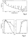
- FIG. 3 shows the overview spectrum of a photoelectron spectroscopy measurement (XPS measurement) of a silicon layer processed identically to sample A3. Plotted is the intensity (intensity) in normalized unit over the binding energy (binding energy) in eV. The names of the peaks are composed of the element abbreviation and the shell specification or Auger transition.
- the XPS spectrum also has signals of the elements Cd, Zn, S and O. About the energetic position of the signals can be concluded on the connection. It is very likely that the layer is a mixture of CdS and ZnO. The compounds CdO and ZnS can be excluded. Thus, the ILGAR process performed did not result in conversion of the CdS particles. Diffusion of the sulfur with subsequent formation of ZnS from the prepared ZnO matrix also did not occur. Thus, clearly CdS particles were embedded in an ILGAR-ZnO matrix.
- FIG. 4 shows the transmission behavior of a ZnO window layer (curve A).
- the right diagram shows an enlargement of the left diagram.
- the transmission is plotted in% over the wavelength ⁇ in nm.
- the absorption edge is clearly visible at approx. 375 nm, and there are also strong interferences (oscillations in curve A).
- the application of a CdS-particle-doped ILGAR-ZnO layer prepared on the above-mentioned synthesis example on this window layer causes a clear blue shift of the absorption edge (curve B).
- the absorption edge of the window has remained unchanged, by fluorescence, however, a portion of the UV light has been converted into visible light, which increases the transmission.
- solar cells comprising fluorescent particles-containing ILGAR layers prepared according to the present invention can be conceived and have a high degree of conversion.
Landscapes
- Photovoltaic Devices (AREA)
- Luminescent Compositions (AREA)
Applications Claiming Priority (2)
| Application Number | Priority Date | Filing Date | Title |
|---|---|---|---|
| DE10339824A DE10339824B4 (de) | 2003-08-24 | 2003-08-24 | Beschichtungsverfahren zur Deposition und Fixierung von Partikeln auf einer Substratoberfläche und Solarzellen mit funkionellem Schichtenaufbau |
| DE10339824 | 2003-08-24 |
Publications (2)
| Publication Number | Publication Date |
|---|---|
| EP1511087A2 true EP1511087A2 (fr) | 2005-03-02 |
| EP1511087A3 EP1511087A3 (fr) | 2007-08-15 |
Family
ID=34089255
Family Applications (1)
| Application Number | Title | Priority Date | Filing Date |
|---|---|---|---|
| EP04090308A Withdrawn EP1511087A3 (fr) | 2003-08-24 | 2004-08-06 | Procédé de dépot de particules sur une surface de substrate et cellules solaires avec des couches fonctionelles |
Country Status (2)
| Country | Link |
|---|---|
| EP (1) | EP1511087A3 (fr) |
| DE (1) | DE10339824B4 (fr) |
Cited By (1)
| Publication number | Priority date | Publication date | Assignee | Title |
|---|---|---|---|---|
| US8613973B2 (en) | 2007-12-06 | 2013-12-24 | International Business Machines Corporation | Photovoltaic device with solution-processed chalcogenide absorber layer |
Family Cites Families (4)
| Publication number | Priority date | Publication date | Assignee | Title |
|---|---|---|---|---|
| JP2967908B2 (ja) * | 1994-09-21 | 1999-10-25 | 矢崎総業株式会社 | 分散めっき法と太陽電池の製造方法 |
| DE19831214C2 (de) * | 1998-03-19 | 2003-07-03 | Hahn Meitner Inst Berlin Gmbh | Verfahren und Anordnung zur Herstellung dünner Metallchalkogenid-Schichten |
| US6127202A (en) * | 1998-07-02 | 2000-10-03 | International Solar Electronic Technology, Inc. | Oxide-based method of making compound semiconductor films and making related electronic devices |
| DE19916403C1 (de) * | 1999-04-06 | 2000-10-12 | Hahn Meitner Inst Berlin Gmbh | Verfahren zur Herstellung dünner, schwer löslicher Beschichtungen |
-
2003
- 2003-08-24 DE DE10339824A patent/DE10339824B4/de not_active Expired - Fee Related
-
2004
- 2004-08-06 EP EP04090308A patent/EP1511087A3/fr not_active Withdrawn
Cited By (2)
| Publication number | Priority date | Publication date | Assignee | Title |
|---|---|---|---|---|
| US8613973B2 (en) | 2007-12-06 | 2013-12-24 | International Business Machines Corporation | Photovoltaic device with solution-processed chalcogenide absorber layer |
| US9324890B2 (en) | 2007-12-06 | 2016-04-26 | Globalfoundries Inc. | Photovoltaic device with solution-processed chalcogenide absorber layer |
Also Published As
| Publication number | Publication date |
|---|---|
| DE10339824B4 (de) | 2005-07-07 |
| EP1511087A3 (fr) | 2007-08-15 |
| DE10339824A1 (de) | 2005-03-24 |
Similar Documents
| Publication | Publication Date | Title |
|---|---|---|
| DE112010004154B4 (de) | Verfahren zum Herstellen einer Halbleiter-Dünnschicht und einerphotovoltaischen Einheit, welche die Dünnschicht enthält | |
| DE69710614T2 (de) | Verfahren zur herstellung von metalleingelagerten fullerenähnlichen metallchalcogeniden | |
| DE112012003297B4 (de) | Deckschichten für verbesserte Kristallisation | |
| DE69325055T2 (de) | Orientierte polykristalline dünne Filme aus Übergangsmetallchalcogeniden | |
| WO2004052998A1 (fr) | Particules nanometriques noyau-enveloppe et leur production | |
| WO2008074298A1 (fr) | Procédé de préparation de points quantiques incorporés dans une matrice et points quantiques incorporés dans une matrice et préparés à l'aide du procédé | |
| EP2140958A2 (fr) | Procédé de fabrication de dispersions de nanoparticules de métal et produits en étant issu | |
| DE102007014538A1 (de) | Verfahren zur Erzeugung einer Antireflexionsoberfläche auf einem optischen Element sowie optische Elemente mit einer Antireflexionsoberfläche | |
| EP4126352A1 (fr) | Matériau particulaire à action photocatalytique à base de sulfure de zinc, son procédé de production et son utilisation | |
| EP2351087A1 (fr) | Nanofils à la surface d'un substrat, leur procédé de fabrication et d'utilisation | |
| DE102010003414A1 (de) | Verfahren zur Herstellung einer Solarzelle vom Chalcopyrit-Typ | |
| DE60314650T2 (de) | Verfahren zur herstellung von lösungen zur verwendung als beschichtung in photokatalytischen und transparenten filmen | |
| DE10131173C2 (de) | Verfahren zur Herstellung von Kern-Hülle-Teilchen und deren Verwendung | |
| DE102009035797A1 (de) | Verfahren zur Herstellung von Beschichtungen mit Antireflexionseigenschaften | |
| DE102009009550A1 (de) | Verfahren zum nasschemischen Synthetisieren von Dikupfer-Zink-Zinn-Tetrasulfid und/oder - Tetraselenid (CZTS), ein Verfahren zum Herstellen einer Halbleiterschicht aus CZTS sowie eine kolloidale Suspension | |
| DE10339824B4 (de) | Beschichtungsverfahren zur Deposition und Fixierung von Partikeln auf einer Substratoberfläche und Solarzellen mit funkionellem Schichtenaufbau | |
| DE102009054973A1 (de) | Chalkopyrit-Dünnschicht-Solarzelle mit CdS/(Zn(S,O)-Pufferschicht und dazugehöriges Herstellungsverfahren | |
| DE19722474A1 (de) | Verfahren zur Herstellung einer CIS-Dünnfilm-Solarzelle und Verfahren zur Bildung einer ternären Kupfer-Indium-Selen-Legierung | |
| DE10164904B4 (de) | Verfahren zur Herstellung eines Kern-Hülle-Teilchens, wobei der Kern ein nanoskaliges Teilchen ist und die Verwendung des Teilchens | |
| DE112021006938T5 (de) | Photoelektrisches Umwandlungselement einschliesslich eines Übergangsmetallchalkogenid-Dünnfilms und Lichtempfangselement einschliesslich des photoelektrischen Umwandlungselements | |
| DE102021113087A1 (de) | Verfahren zur herstellung von atomaren dünnschichten aus übergangsmetalloxiden und/oder -hydroxiden | |
| DE102008037177B4 (de) | Verfahren zur Herstellung nanostrukturierter Metalloxide oder -chalkogenide mittels chemischer Badabscheidung | |
| AT521545B1 (de) | Suspension zur herstellung einer halbleiterschicht | |
| DE2048497A1 (de) | Lichtträger mit Farbfilter Beschich tung | |
| DE69823004T2 (de) | Verfahren zur Herstellung von Metallenthaltenden Kolloidalen und Verfahren zur Herstellung von Metalloxyden enthaltenden empfindlichen Schichten für chemisches Sensorgerät |
Legal Events
| Date | Code | Title | Description |
|---|---|---|---|
| PUAI | Public reference made under article 153(3) epc to a published international application that has entered the european phase |
Free format text: ORIGINAL CODE: 0009012 |
|
| AK | Designated contracting states |
Kind code of ref document: A2 Designated state(s): AT BE BG CH CY CZ DE DK EE ES FI FR GB GR HU IE IT LI LU MC NL PL PT RO SE SI SK TR |
|
| AX | Request for extension of the european patent |
Extension state: AL HR LT LV MK |
|
| PUAL | Search report despatched |
Free format text: ORIGINAL CODE: 0009013 |
|
| AK | Designated contracting states |
Kind code of ref document: A3 Designated state(s): AT BE BG CH CY CZ DE DK EE ES FI FR GB GR HU IE IT LI LU MC NL PL PT RO SE SI SK TR |
|
| AX | Request for extension of the european patent |
Extension state: AL HR LT LV MK |
|
| 17P | Request for examination filed |
Effective date: 20080215 |
|
| AKX | Designation fees paid |
Designated state(s): AT BE BG CH CY CZ DE DK EE ES FI FR GB GR HU IE IT LI LU MC NL PL PT RO SE SI SK TR |
|
| RAP1 | Party data changed (applicant data changed or rights of an application transferred) |
Owner name: HELMHOLTZ-ZENTRUM BERLIN FUER MATERIALIEN UND ENER |
|
| STAA | Information on the status of an ep patent application or granted ep patent |
Free format text: STATUS: THE APPLICATION IS DEEMED TO BE WITHDRAWN |
|
| 18D | Application deemed to be withdrawn |
Effective date: 20090301 |