EP1511363A1 - Organische feldemissionsvorrichtung und feldemissionsvorrichtung - Google Patents
Organische feldemissionsvorrichtung und feldemissionsvorrichtung Download PDFInfo
- Publication number
- EP1511363A1 EP1511363A1 EP02730838A EP02730838A EP1511363A1 EP 1511363 A1 EP1511363 A1 EP 1511363A1 EP 02730838 A EP02730838 A EP 02730838A EP 02730838 A EP02730838 A EP 02730838A EP 1511363 A1 EP1511363 A1 EP 1511363A1
- Authority
- EP
- European Patent Office
- Prior art keywords
- light emission
- layer
- light emitting
- organic electroluminescence
- compound
- Prior art date
- Legal status (The legal status is an assumption and is not a legal conclusion. Google has not performed a legal analysis and makes no representation as to the accuracy of the status listed.)
- Withdrawn
Links
Images







Classifications
-
- H—ELECTRICITY
- H10—SEMICONDUCTOR DEVICES; ELECTRIC SOLID-STATE DEVICES NOT OTHERWISE PROVIDED FOR
- H10K—ORGANIC ELECTRIC SOLID-STATE DEVICES
- H10K50/00—Organic light-emitting devices
- H10K50/10—OLEDs or polymer light-emitting diodes [PLED]
- H10K50/11—OLEDs or polymer light-emitting diodes [PLED] characterised by the electroluminescent [EL] layers
-
- H—ELECTRICITY
- H05—ELECTRIC TECHNIQUES NOT OTHERWISE PROVIDED FOR
- H05B—ELECTRIC HEATING; ELECTRIC LIGHT SOURCES NOT OTHERWISE PROVIDED FOR; CIRCUIT ARRANGEMENTS FOR ELECTRIC LIGHT SOURCES, IN GENERAL
- H05B33/00—Electroluminescent light sources
- H05B33/12—Light sources with substantially two-dimensional [2D] radiating surfaces
- H05B33/14—Light sources with substantially two-dimensional [2D] radiating surfaces characterised by the chemical or physical composition or the arrangement of the electroluminescent material, or by the simultaneous addition of the electroluminescent material in or onto the light source
Definitions
- the present invention relates to an organic electroluminescence light emitting device (organic EL device) including an organic layer having a light emitting region between an anode and a cathode, and to a light emitting apparatus, such as a display device, using the same.
- organic EL device organic electroluminescence light emitting device
- Displays have a major role in our daily living, for example, in the forms of television receivers, computer monitors, and portable information terminals.
- displays as human interfaces have become increasingly important. These displays have been required to have a screen being comfortable for eyes to see and ensuring a definition high enough to allow clear viewing, and to have a resolution and a responsiveness high enough to allow clear, clean viewing of moving pictures without delay.
- Organic EL devices using organic compounds as luminescent materials exhibit a wide viewing angle, a high contrast, and an excellent visibility. Another advantage of organic EL devices is that since the devices emit spontaneous light, they do not require any backlight unlike liquid crystal, to thereby realize thinning of the size and reduction in weight, and also realize reduction in power consumption.
- Organic EL devices using organic compounds as luminescent materials are further advantageous in that they are operable with a low DC voltage at a high response speed, have a resistance against vibration, and are usable in a wide range of temperatures.
- Organic EL devices therefore, have become a focus of attention as the next generation display devices, and some of them have already begun to be put into market.
- Organic electroluminescence light emitting devices using organic luminescent materials have a configuration that an organic electroluminescence layer containing an organic luminescent material is sandwiched between an anode and a cathode, wherein at least one of the anode and the cathode has a light permeability. In these devices, light emission occurs when a DC voltage is applied between the anode and the cathode.
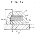
- FIGS. 10 and 12 show examples of related art organic electroluminescence light emitting devices (organic EL devices).
- FIG. 10 shows a related art organic electroluminescence light emitting device having a single-hetero structure, wherein an anode 6 made from a light permeable ITO (Indium Tin Oxide) or the like, an organic layer 15a composed of a hole transport layer 2 and an electron transport layer 4, and a cathode 7 are sequentially stacked on a substrate 10 made from light permeable glass or the like, and the stacked structure thus formed on the substrate 10 is sealed with a protective layer 14.
- a DC voltage supplied from a power source 20 is applied between the anode 6 and the cathode 7, light 5 having a specific wavelength is emitted from an interface between the hole transport layer 2 and the electron transport layer 4.
- FIG. 11 shows another organic electroluminescence light emitting device having a double-hetero structure, wherein a light permeable anode 6, an organic layer 15b composed of a hole injection layer 1, a hole transport layer 2, a light emission layer 3, and an electron transport layer 4, and a cathode 7 are sequentially stacked on a light permeable substrate 10, and the stacked structure formed on the substrate 10 is sealed with a protective layer 14.
- the hole injection layer is not necessarily provided.
- FIG. 12 is a view showing a configuration of a flat display using the above-described organic electroluminescence light emitting device.
- an organic layer 15 (15a, 15b) allowing emission of light of three primary colors of red (R), green (G), and blue (B) is disposed between a cathode 7 and an anode 6.
- the cathode 7 is composed of cathode stripes 7
- the anode 6 is composed of anode stripes 6, wherein the cathode stripes 7 and the anode stripes 6 are arranged to cross each other.
- a signal voltage is selectively applied from a luminance signal circuit 24 to one of the cathode stripes 7 and a signal voltage is selectively applied from a shift register integrated control circuit 25 to one of the anode stripes 6, whereby a portion (pixel) of the organic layer, located at a position where the selected cathode stripe 7 and the selected anode stripe 6 cross each other, emits light.
- the light emission layer can be made from one kind or two or more kinds of materials selected from various materials.
- a device structure for example, of a type shown in FIG. 10, characterized by including a light emission layer made from two or more kinds of materials, a two-layer structure having an electron transport layer 4 containing a luminescent material so as to serve as a light emission layer and a hole transport layer 2 has been reported by C. W. Tang, S. A. VanSlyke, and C. H. Chen in J. of Appl. Phys. 65-9, 3610-3616 (1989). This device structure has been also disclosed in Japanese Patent Laid-open No. Sho 63-264692.
- a light emission layer is composed of an organic host material capable of sustaining injection of both holes and electrons, and a fluorescent material capable of emitting light in response to hole-electron recombination.
- the hue of light emitted from the light emission layer is modified by doping a slight amount of such a fluorescent material in the light emission layer.
- the minimum amount, being enough to achieve the above-described effect, of the fluorescent material varies depending on specific selection of the host material and the fluorescent material; however, according to the above-described known technique, it is described in the specification of the patent document that in any case, it is not required to use the fluorescent material in an amount of about 10 mole percent or more on the basis of the mole number of the host material, and more specifically, it is seldom required to use the fluorescent material in an amount of 1 mole percent or more.
- the emission wavelength (535 nm) of the EL device including the light emission layer containing no fluorescent material becomes longer with the increase in concentration of the fluorescent material, and the emission wavelength of the EL device reaches 690 nm when the concentration of the fluorescent material is 4 mole percent.
- the EL device produced by the above-described cited technique has some advantages.
- One of the advantages is to easily change the emission wavelength.
- the EL device including the light emission layer made from a single luminescent material in order to change the emission color, it is required to change a chemical structure of the luminescent material, and therefore, in order to introduce each substitutional group for changing the emission wavelength, it is required to synthesize a new material.
- the emission wavelength can be changed by doping a slight amount of a fluorescent material in the host material.
- Another advantage is that a fluorescent material having neither film formability nor charge transport characteristic can be used.
- the known technique however, has important problems from the viewpoint of practical use.
- One of the problems is that since the hue and the luminous efficiency are greatly varied depending on a variation in concentration of the fluorescent material as described in the specification of the patent document, it is difficult to perform quality control for keeping the characteristics in the production process.
- Another problem is that since the hue is varied depending on an applied voltage or current, it is difficult to stably control the hue in the case where the device is applied as an element of a display.
- holes and electrons are concentrated at an interface between the organic layers 2 and 4 or its vicinity, or concentrated at an interface between the organic layers 2 and 3 and its vicinity, or an interface between the organic layers 3 and 4 and its vicinity, and consequently, light emission occurs at the interface or its vicinity, causing deterioration of the device, thereby shortening the service life of the device. In other words, the device having the above structure is poor in reliability.
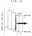
- the light emission layer 3 is made from a single material having an electron transport characteristic, as shown in FIG.
- a region (light emission region) in which hole-electron recombination efficiently occurs is concentrated in the vicinity of an interface, adjacent to a hole transport layer, of the light emission layer; and if the light emission layer 3 is made from a single material having a hole transport characteristic, as shown in FIG. 14 illustrating energy levels of layers constituting the device, a light emission region is concentrated in the vicinity of an interface, adjacent to an electron transport layer, of the light emission layer.
- an object of the present invention is to provide an organic electroluminescence light emitting device capable of preventing a color (hue) of light and a luminous efficiency from being varied depending on a concentration of a luminous material contained in a light emission layer and an operational condition such as an applied voltage, thereby exhibiting a high luminance, a high performance, and a stable, high reliability.
- an organic electroluminescence light emitting device in which an organic layer having a light emission region is provided between an anode and a cathode, characterized in that at least one of layers constituting the organic layer is composed of a mixed layer made from a luminescent material and a charge injection accelerating material, wherein the luminescent material exhibits, in a state held as a single thin film between the anode and the cathode, electroluminescence light emission when a voltage is applied thereto and has a charge transport characteristic, and the charge injection accelerating material has a charge transport characteristic capable of accelerating injection of charges in the luminescent material; and the at least one of layers constituting the organic layer has a light emission region existing not only at an interface with an adjacent layer or its vicinity but also over a specific thickness region from the interface or its vicinity in the layer thickness direction.
- the present invention also provides a light emitting a light emitting a light emission region existing not only at an interface with an adjacent layer or its vicinity but also over a specific thickness region from the interface or
- the organic electroluminescence light emitting device of the present invention typically includes an anode, a hole transport layer, a light emission layer, an electron transport layer, or includes an anode, a hole transport layer, and a light emission layer serving as an electron transport layer.
- a light emission region of the device is formed by a mixed layer made from a luminescent material and a charge injection accelerating material.
- the luminescent material exhibits, in a state held as a single thin film between the anode and the cathode, electroluminescence light emission when a DC voltage is applied thereto and has a charge transport characteristic.
- the charge injection accelerating material is different from the luminous material and has a charge transport characteristic capable of accelerating injection of charges in the luminescent material.
- the light emission region exists not only at an interface with an adjacent layer or its vicinity but also over a specific thickness region in the layer thickness direction. Accordingly, a region in which light is emitted is not limited to the above-described interface or its vicinity but can be spread in a wide range of the light emission layer. This means that even if the performance of a portion located in the layer thickness direction is deteriorated, light emission occurs a portion above or below the deteriorated portion, so that light emission occurs substantially over a specific thickness region in the light emission layer. As a result, it is possible to significantly improve the service life of the device.
- the luminous material used for the above-described known technique exhibits light emission resulting from fluorescence.
- the luminous material used for the present invention exhibits, in a state held as a single thin film between an anode and a cathode, electroluminescence light emission by itself when a DC voltage is applied thereto.
- the luminous material used for the present invention has not only electroluminescence light emission characteristic but also a charge transport characteristic, and therefore, does not require a material equivalent to the host material (used in the known technique) for keeping injection of holes and electrons in the light emission layer, and further the luminous material does not emit light in response to hole-electron recombination but emits light by performing hole-electron recombination by itself. Accordingly, a hue and a luminous efficiency of the device of the present invention is not varied so much depending on a concentration of the luminous material, with a result that the device of the present invention can obtain a stable hue.
- the above-described thickness region is preferably specified such that on the basis of an intensity of light emitted from each or both of an interface between the mixed layer and an electron transport layer adjacent thereto and an interface between the mixed layer and a hole transport layer adjacent thereto, an intensity of light emitted from a position being equidistant from the both interfaces is in a range of 25% or more.
- a concentration range of the luminous material on the basis of a mole number of the charge injection accelerating material having a charge transport characteristic capable of accelerating injection of charges in the luminous material in the light emission layer is preferably in a range of 5 to 90 mole percent (about 5 to 90 wt%), more preferably, in a range of 10 to 90 mole percent (about 10 to 90 wt%).
- the minimum ratio of the fluorescent material is varied depending on the specific selection of the host material and the fluorescent material; however, in any case, it is not required to use the fluorescent material in an amount of about 10 mole percent or more on the basis of the mole number of the host material, and more specifically, it is seldom required to use the fluorescent material in an amount of 1 mole percent or more. Therefore, the ratio of the fluorescent material is substantially not overlapped to the preferred concentration range of the luminous material used for the present invention. Further, according to the present invention, a hue of light is not varied depending on a change in the applicable concentration of the luminous material. This is basically different from the known technique intended to positively change a hue of light by changing the concentration of the fluorescent material.
- the charge injection accelerating material having a charge transport characteristic capable of accelerating injection of charges in the light emission layer for acceleration light emission due to hole-electron recombination in the luminous material is preferably specified as follows: (1) an energy level of a lowest unoccupied molecular orbital (LUMO) of the charge injection accelerating material is equal to or smaller (shallower) than that of the luminous material, or an energy level of a highest occupied molecular orbital (HOMO) of the charge injection accelerating material is equal to or larger (deeper) than that of the luminous material; or (2) the energy level of the lowest unoccupied molecular orbital (LUMO) of the charge injection accelerating material is equal to or smaller (shallower) than that of the luminous material, and the energy level of the highest occupied molecular orbital (HOMO) of the charge injection accelerating material is equal to or larger (deeper) than that of the luminous material.
- LUMO lowest unoccupied molecular orbital
- HOMO highest occupied molecular orbital
- the same material as a material forming the electron transport layer can be used as a material having the charge transport characteristic capable of accelerating injection of charges in the luminous material
- the same material as a material forming the hole transport layer can be used as a material having the charge transport characteristic capable of injection of charges in the luminous material.
- both the same material as a material forming the electron transport layer and the same material as a material forming the hole transport layer can be used as the material having the charge transport characteristic capable of accelerating injection of charges in the luminous material.
- an energy level of the lowest unoccupied molecular orbital (LUMO) of the hole transport layer adjacent to the mixed layer may be shallower than that of each of the luminous material and the charge injection accelerating material.
- LUMO lowest unoccupied molecular orbital
- the organic electroluminescence light emitting device of the present invention does not make use of a mechanism that either or both of electrons injected from the cathode and holes injected from the anode are concentrated at the interface between the organic layers, to cause hole-electron recombination, resulting in light emission, but make use of a mechanism that the luminous material efficiently acts as a trap for electrons and holes in the material having the charge transport characteristic in the light emission layer, to cause hole-electron recombination in the luminous material, resulting in light emission.
- the organic electroluminescence light emitting device of the present invention is thus characterized in that the light emission region is not concentrated in the vicinity of the interface between the organic layers but can exist over a wide range in the light emission layer, so that as compared with the case where a luminous material singly exists in a light emission layer, it is possible to significantly improve the reliability of the device.
- the light emitting device of the present invention it is possible to prevent occurrence of an inconvenience that the concentrated charge density in a light emission layer of a device accelerates deterioration of the device.
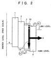
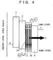
- a region (light emission region) in which recombination 8 of holes and electrons efficiently occurs is concentrated in the vicinity of an interface of a portion in the light emission layer 3 with a hole transport layer 2.
- a light emission region is concentrated in the vicinity of an interface of a portion in the light emission layer 3 with an electron transport layer 4.
- a region (light emission region) in which recombination 19 of holes and electrons efficiently occurs is somewhat spread inwardly from the interface into the light emission layer (within a specific thickness region in the layer thickness direction).
- the distribution of a light emission region in the light emission layer is varied depending on a voltage and a current applied to the device and a luminance; however, at an effective available luminance necessary for a display or the like using the device, the light emission region in the light emission layer is preferably specified such that on the basis of an intensity of light emitted from each or both of an interface between the mixed layer and an electron transport layer adjacent thereto and an interface between the mixed layer and a hole transport layer adjacent thereto, an intensity of light emitted from a position being equidistant from the both interfaces, that is, from a central portion of the light emission layer is in a range of 25% or more.
- the charge injection accelerating material may have not only the electron transport characteristic but also the hole transport characteristic, and the luminous material may have not only the hole transport characteristic but also the electron transport characteristic.
- the charge injecting accelerating material may have not only the hole transport characteristic but also the electron transport characteristic, and the luminous material may have not only the electron transport characteristic but also the hole transport characteristic.
- organic electroluminescence light emitting device of the present invention may be used as at least part of each of pixels of a display.
- FIG. 10 shows the above-described device structure including the anode 6, the hole transport layer 2, the light emission layer 4 serving as an electron transport layer, and the cathode 7, and
- FIG. 11 shows the above-described device structure including the anode 6, the hole injection layer 1 (provided as needed), the hole transport layer 2, the light emission layer 3, the electron transport layer 4, and the cathode 7.
- the organic electroluminescence light emitting device of the present invention is applicable to each of these device structures; however, as shown in FIGS. 1 to 4, according to the present invention, a charge (electron or hole) injection accelerating material is mixed in the light emission layer.
- a voltage is applied between the anode 6 and the cathode 7 of the device having the above device structure, a current flows therebetween, to allow light emission from the light emission layer of the device.
- a substrate 10 for supporting the organic electroluminescence light emitting device is in contact with the anode 6 or the cathode 7.
- a light permeable substrate made from glass, quartz, or plastic, a substrate having no light permeability in a visible light region such as silicon, or a substrate on the surface of which a thin film transistor circuit is formed is used in accordance with an application of the device.
- the anode 6 may be made from ITO (Indium Tin Oxide), a metal such as SnO 2 , Cr, Pd, In, Au, W, or Ni, or an alloy containing one of the metals.
- the cathode 7 may be made from an active metal such as Li, Mg or Ca, or an alloy containing Ag, Al, or In and one of the active metals. In addition, the cathode 7 may be of a stacked structure of these metal or alloy layers.
- the above materials for the anode 6 and the cathode 7 are only for illustrative purposes only, and it is to be understood that other materials may be used in accordance with an application of the device. Further, to improve the service life of the organic electroluminescence light emitting device, the device may be provided with a means for cutting off permeation of water or oxygen from external.
- the hole injection layer 1 for accelerating injection of holes may be provided between the anode 6 and the hole transport layer 2.
- the hole injection layer 1 may be made from, for example, a porphyrin compound described in U.S. Patent No. 4,720,432.
- the hole transport may be of not a single layer but a stacked structure.
- Each of the electron transport layer and the hole transport layer may be made from a material suitably selected from known materials.
- a thin film made from LiF or LiO 2 may be inserted.
- a hole block layer for preventing injection of holes from the light emission layer to the electron transport layer may be provided.
- a luminous material contained in the light emission layer there is known a material having, in its molecular skeleton, a styryl or distyryl structure described in Japanese Patent Laid-open Nos. Hei 11-329730, Hei 11-329731, 2000-91076, 2000-173773, 2000-12224, 2000-12225, 2000-12226, 2000-12227, 2000-12228, 2000-91073, 2000-91074, 2000-91075, 2000-173774, 2001-110570, and 2001-110571.
- Such a material can satisfy the prerequisite of the present invention that it has formability of an amorphous thin film and exhibits, in a state held as a single thin film between the anode and the cathode, electroluminescence light emission when a DC voltage is applied thereto.
- charge injection accelerating material capable of accelerating injection of charges in the luminous material
- a material having a charge transport characteristic capable of accelerating injection of charges in the luminous material
- a material suitably selected from known electron transport materials and hole transport materials there may be used a material suitably selected from known electron transport materials and hole transport materials.
- organic electroluminescence light emitting devices each using, as a light emission layer having an electron transport characteristic, a mixed layer made from a styryl compound represented by a compound 1 described below and an electron transport material represented by Alq 3 (tris (8-quinolinol) aluminum) described below, are produced as samples, and a relationship between a luminance of light emitted from each sample and a luminous efficiency of the sample is examined.
- a mixed layer made from a styryl compound represented by a compound 1 described below and an electron transport material represented by Alq 3 (tris (8-quinolinol) aluminum) described below are produced as samples, and a relationship between a luminance of light emitted from each sample and a luminous efficiency of the sample is examined.
- Samples of organic electroluminescence light emitting devices were prepared as follows: namely, as a light emission layer of each organic electroluminescence light emitting device, a mixed layer made from a styryl compound 1 expressed by the following chemical formula, and an electron transport material Alq 3 expressed by the following chemical formula was formed by a vacuum vapor-deposition process; and as the other components of this light emitting device, a glass sheet was used as a substrate, and an anode made from ITO, a hole transport layer made from ⁇ -NPD expressed by the following chemical formula, and a cathode made from Mg-Ag were each formed by a known process.
- Device structures of the samples thus prepared are shown below. It is to be noted that in each device structure, a value in the parenthesis expresses a film thickness (the same applies in the later examples).
- a relationship between a luminance and a luminous efficiency of each of the sample Nos. Device (1-1), Device (1-2), Device (1-3), Device (1-4), and Device (1-5) is shown in Table 1. It is to be noted that the luminous efficiency is calculated as a rate of luminance to a current value.
- organic electroluminescence light emitting devices each using, as a light emission layer having a hole transport characteristic, a mixed layer made from the same styryl compound 1 as that described in Example 1 and the same hole transport material ⁇ -NPD as that described in Example 1, are produced as samples, and a relationship between a luminance of light emitted from each sample and a luminous efficiency of the sample is examined.
- Samples of organic electroluminescence light emitting devices were prepared in the same manner as that described in Example 1, except that a mixed layer made from the same styryl compound 1 as that described in Example 1 and the same hole transport material ⁇ -NPD as that described in Example 1 was formed as a light emission layer by a vacuum vapor-deposition process.
- a relationship between a luminance and a luminous efficiency of each of the sample Nos. Device (2-1), Device (2-2), Device (2-3), Device (2-4), and Device (2-5) is shown in Table 2. It is to be noted that the luminous efficiency is calculated as a rate of luminance to a current value.
- organic electroluminescence light emitting devices each using, as a light emission layer having an electron transport characteristic, a mixed layer made from a styryl compound represented by a compound 2 described below and the same electron transport material Alq 3 (tris (8-quinolinol) aluminum) as that described in Example 1, are produced as samples, and a relationship between a luminance of light emitted from each sample and a luminous efficiency of the sample is examined.
- Samples of organic electroluminescence light emitting devices were prepared in the same manner as that described in Example 1, except that a mixed layer made from a styryl compound represented by a compound 2 expressed by the following chemical formula and the same electron transport material Alq 3 as that described in Example 1 was formed as a light emission layer by a vacuum vapor-deposition process.
- a relationship between a luminance and a luminous efficiency of each of the sample Nos. Device (3-1), Device (3-2), Device (3-3), Device (3-4), and Device (3-5) is shown in Table 3. It is to be noted that the luminous efficiency is calculated as a rate of luminance to a current value.
- organic electroluminescence light emitting devices each using, as a light emission layer having a hole transport characteristic, a mixed layer made from the same styryl compound 2 as that described in Example 2 and the same hole transport material ⁇ -NPD as that described in Example 1, are produced as samples, and a relationship between a luminance of light emitted from each sample and a luminous efficiency of the sample is examined.
- Samples of organic electroluminescence light emitting devices were prepared in the same manner as that described in Example 1, except that a mixed layer made from the same styryl compound 2 as that described in Example 2 and the same hole transport material ⁇ -NPD as that described in Example 1 was formed as a light emission layer by a vacuum vapor-deposition process.
- organic electroluminescence light emitting devices each using, as a light emission layer having an electron transport characteristic, a mixed layer made from the same styryl compound 1 as that described in Example 1 and the same electron transport material Alq 3 as that described in Example 1, are produced as samples, and a relationship between a luminance of light emitted from each sample and a hue of the light emitted from the sample is examined.
- Samples of organic electroluminescence light emitting devices were prepared in the same manner as that described in Example 1. Namely, like Example 1, a mixed layer made from the same styryl compound 1 as that described in Example 1 and the same electron transport material Alq 3 as that described in Example 1 was formed as a light emission layer by a vacuum vapor-deposition process. The same sample Nos. Device (1-1), Device (1-2), Device (1-3), Device (1-4), and Device (1-5) as those prepared in Example 1 were thus prepared.
- organic electroluminescence light emitting devices each using, as a light emission layer having a hole transport characteristic, a mixed layer made from the same styryl compound 1 as that described in Example 2 and the same hole transport material ⁇ -NPD as that described in Example 2, are produced as samples, and a relationship between a luminance of light emitted from each sample and a hue of the light emitted from the sample is examined.
- Samples of organic electroluminescence light emitting devices were prepared in the same manner as that described in Example 2. Namely, like Example 2, a mixed layer made from the same styryl compound 1 as that described in Example 2 and the same hole transport material ⁇ -NPD as that described in Example 2 was formed as a light emission layer by a vacuum vapor-deposition process. The same sample Nos. Device (2-1), Device (2-2), Device (2-3), Device (2-4), and Device (2-5) as those prepared in Example 2 were thus prepared. A relationship between a luminance and a hue of each of the samples is shown in Table 6.
- organic electroluminescence light emitting devices each using, as a light emission layer having an electron transport characteristic, a mixed layer made from the same styryl compound 2 as that described in Example 3 and the same electron transport material Alq 3 as that described in Example 3, are produced as samples, and a relationship between a luminance of light emitted from each sample and a hue of the light emitted from the sample is examined.
- Samples of organic electroluminescence light emitting devices were prepared in the same manner as that described in Example 3. Namely, like Example 3, a mixed layer made from the same styryl compound 2 as that described in Example 3 and the same electron transport material Alq 3 as that described in Example 3 was formed as a light emission layer by a vacuum vapor-deposition process. The same sample Nos. Device (3-1), Device (3-2), Device (3-3), Device (3-4), and Device (3-5) as those prepared in Example 3 were thus prepared. A relationship between a luminance and a hue of each of the samples is shown in Table 7.
- organic electroluminescence light emitting devices each using, as a light emission layer having a hole transport characteristic, a mixed layer made from the same styryl compound 2 as that described in Example 4 and the same hole transport material ⁇ -NPD as that described in Example 4, are produced as samples, and a relationship between a luminance of light emitted from each sample and a hue of the light emitted from the sample is examined.
- Samples of organic electroluminescence light emitting devices were prepared in the same manner as that described in Example 4. Namely, like Example 4, a mixed layer made from the same styryl compound 2 as that described in Example 4 and the same hole transport material ⁇ -NPD as that described in Example 4 was formed as a light emission layer by a vacuum vapor-deposition process. The same sample Nos. Device (4-1), Device (4-2), Device (4-3), Device (4-4), and Device (4-5) as those prepared in Example 4 were thus prepared. A relationship between a luminance and a hue of each of the samples is shown in Table 8.
- an organic electroluminescence light emitting device using, as a light emission layer having an electron transport characteristic, a mixed layer made from the same styryl compound 1 as that described in Example 1 and the same electron transport material Alq 3 as that described in Example 1 is produced as a sample, and a reliability of the sample is examined.
- Example 1 A sample of an organic electroluminescence light emitting device was prepared in the same manner as that described in Example 1. Namely, like Example 1, a mixed layer made from the same styryl compound 1 as that described in Example 1 and the same electron transport material Alq 3 as that described in Example 1 was formed as a light emission layer by a vacuum vapor-deposition process. The same sample No. Device (1-3) as that prepared in Example 1 was thus prepared.
- the sample thus prepared was left in a nitrogen atmosphere for one month, the result of which showed that no deterioration of the sample was observed.
- the sample was also forcibly deteriorated by continuously applying a constant current thereto with an initial luminance set to 1,000 cd/m 2 so as to continuously emit light, the result of which showed that the half value period of luminance was 1,000 hours.
- an organic electroluminescence light emitting device using, as a light emission layer having an electron transport characteristic, a mixed layer made from the same styryl compound 2 as that described in Example 3 and the same electron transport material Alq 3 as that described in Example 3 is produced as a sample, and a reliability of the sample is examined.
- Example 3 A sample of an organic electroluminescence light emitting device was prepared in the same manner as that described in Example 3. Namely, like Example 3, a mixed layer made from the same styryl compound 2 as that described in Example 3 and the same electron transport material Alq 3 as that described in Example 3 was formed as a light emission layer by a vacuum vapor-deposition process. The same sample No. Device (3-3) as that prepared in Example 3 was thus prepared.
- the sample thus prepared was left in a nitrogen atmosphere for one month, the result of which showed that no deterioration of the sample was observed.
- the sample was also forcibly deteriorated by continuously applying a constant current thereto with an initial luminance set to 1,000 cd/m 2 so as to continuously emit light, the result of which showed that the half value period of luminance was 4,800 hours.
- organic electroluminescence light emitting devices each using, as a light emission layer having an electron transport characteristic, a mixed layer made from a styryl compound represented by a compound 3 expressed by the following chemical formula and the same electron transport material Alq 3 as that described in Example 1, are produced as samples, and device characteristics of each sample are examined.
- Samples of organic electroluminescence light emitting devices were prepared in the same manner as that for preparing the sample Nos. Device (1-1) to Device (1-5) in Example 1, except that a mixed layer made from a styryl compound represented by a compound 3 having the above chemical formula and the same electron transport material Alq 3 as that described in Example 1 was formed as a light emission layer by a vacuum vapor-deposition process.
- Five sample Nos. Device (11-1), (11-2), (11-3), (11-4), and (11-5) containing 10 wt%, 30 wt%, 50 wt%, 80 wt%, and 90 wt% of the compound 3 in the mixed layer, respectively were thus prepared.
- Each of the five samples emitted light of red, and exhibited a high luminous efficiency in a practical luminance region from 10 to 1,000 cd/m 2 . Also, it was revealed that the sample did not exhibit any change in hue with an increase in luminance, and therefore, the sample was useful as a display device.
- each of the samples thus prepared was left in a nitrogen atmosphere for one month, the result of which showed that no deterioration of the sample was observed.
- the sample No. Device (11-3) was also forcibly deteriorated by continuously applying a constant current thereto with an initial luminance set to 1,000 cd/m 2 so as to continuously emit light, the result of which showed that the half value period of luminance was 1,200 hours.
- organic electroluminescence light emitting devices each using, as a light emission layer having an electron transport characteristic, a mixed layer made from a styryl compound represented by a compound 4 expressed by the following chemical formula and the same electron transport material Alq 3 as that described in Example 1, are produced as samples, and device characteristics of each sample are examined.
- Samples of organic electroluminescence light emitting devices were prepared in the same manner as that for preparing the sample Nos. Device (1-1) to Device (1-5) in Example 1, except that a mixed layer made from a styryl compound represented by a compound 4 having the above chemical formula and the same electron transport material Alq 3 as that described in Example 1 was formed as a light emission layer by a vacuum vapor-deposition process.
- Five sample Nos. Device (12-1), (12-2), (12-3), (12-4), and (12-5) containing 10 wt%, 30 wt%, 50 wt%, 80 wt%, and 90 wt% of the compound 4 in the mixed layer, respectively were thus prepared.
- Each of the five samples emitted light of green, and exhibited a high luminous efficiency in a practical luminance region from 10 to 1,000 cd/m 2 . Also, it was revealed that the sample did not exhibit any change in hue with an increase in luminance, and therefore, the sample was useful as a display device.
- each of the samples thus prepared was left in a nitrogen atmosphere for one month, the result of which showed that no deterioration of the sample was observed.
- the sample No. Device (12-3) was also forcibly deteriorated by continuously applying a constant current thereto with an initial luminance set to 1,000 cd/m 2 so as to continuously emit light, the result of which showed that the half value period of luminance was 500 hours.
- organic electroluminescence light emitting devices each using, as a light emission layer having a hole transport characteristic, a mixed layer made from a styryl compound represented by a compound 5 expressed by the following chemical formula and the same hole transport material ⁇ -NPD as that described in Example 2, are produced as samples, and device characteristics of each sample are examined.
- Samples of organic electroluminescence light emitting devices were prepared in the same manner as that for preparing the sample Nos. Device (2-1) to Device (2-5) in Example 2, except that a mixed layer made from a styryl compound represented by a compound 5 having the above chemical formula and the same hole transport material ⁇ -NPD as that described in Example 2 was formed as a light emission layer by a vacuum vapor-deposition process.
- Five sample Nos. Device (13-1), (13-2), (13-3), (13-4), and (13-5) containing 10 wt%, 30 wt%, 50 wt%, 80 wt%, and 90 wt% of the compound 5 in the mixed layer, respectively were thus prepared.
- Each of the five samples emitted light of blue-green, and exhibited a high luminous efficiency in a practical luminance region from 10 to 500 cd/m 2 . Also, it was revealed that the sample did not exhibit any change in hue with an increase in luminance, and therefore, the sample was useful as a display device.
- each of the samples thus prepared was left in a nitrogen atmosphere for one month, the result of which showed that no deterioration of the sample was observed.
- the sample No. Device (13-3) was also forcibly deteriorated by continuously applying a constant current thereto with an initial luminance set to 500 cd/m 2 so as to continuously emit light, the result of which showed that the half value period of luminance was 800 hours.
- organic electroluminescence light emitting devices each using, as a light emission layer having a hole transport characteristic, a mixed layer made from a compound 6 expressed by the following chemical formula and the same hole transport material ⁇ -NPD as that described in Example 2 and the like, are produced as samples, and device characteristics of each sample are examined.
- Samples of organic electroluminescence light emitting devices were prepared by forming the following layer structures on an ITO substrate by a vacuum vapor-deposition process.
- a second electron transport layer made from BAlq (bis (8-quinolinol) aluminum derivative) expressed by the following chemical formula was additionally formed between the light emission layer and the electron transport layer.
- Each of the five samples emitted light of blue-green, and exhibited a high luminous efficiency in a practical luminance region from 10 to 500 cd/m 2 . Also, it was revealed that the sample did not exhibit any change in hue with an increase in luminance, and therefore, the sample was useful as a display device.
- each of the samples thus prepared was left in a nitrogen atmosphere for one month, the result of which showed that no deterioration of the sample was observed.
- the sample No. Device (14-3) was also forcibly deteriorated by continuously applying a constant current thereto with an initial luminance set to 500 cd/m 2 so as to continuously emit light, the result of which showed that the half value period of luminance was 700 hours.
- organic electroluminescence light emitting devices each using, as a light emission layer having a hole transport characteristic, a mixed layer made from a compound 7 expressed by the following chemical formula and the same hole transport material ⁇ -NPD as that described in Example 14, are produced as samples, and device characteristics of each sample are examined.
- Samples of organic electroluminescence light emitting devices were prepared in the same manner as that for preparing the sample Nos. Device (14-1) to Device (14-5) in Example 14, except that a mixed layer made from a compound 7 having the above chemical formula and the same hole transport material ⁇ -NPD as that described in Example 14 was formed as a light emission layer by a vacuum vapor-deposition process.
- Five sample Nos. Device (15-1), (15-2), (15-3), (15-4), and (15-5) containing 10 wt%, 30 wt%, 50 wt%, 80 wt%, and 90 wt% of the compound 7 in the mixed layer, respectively were thus prepared.
- Each of the five samples emitted light of blue, and exhibited a high luminous efficiency in a practical luminance region from 10 to 500 cd/m 2 . Also, it was revealed that the sample did not exhibit any change in hue with an increase in luminance, and therefore, the sample was useful as a display device.
- each of the samples thus prepared was left in a nitrogen atmosphere for one month, the result of which showed that no deterioration of the sample was observed.
- the sample No. Device (15-3) was also forcibly deteriorated by continuously applying a constant current thereto with an initial luminance set to 500 cd/m 2 so as to continuously emit light, the result of which showed that the half value period of luminance was 600 hours.
- organic electroluminescence light emitting devices each using, as a light emission layer having a hole transport characteristic, a mixed layer made from a compound 8 expressed by the following chemical formula and the same hole transport material ⁇ -NPD as that described in Example 14, are produced as samples, and device characteristics of each sample are examined.
- Samples of organic electroluminescence light emitting devices were prepared in the same manner as that for preparing the sample Nos. Device (14-1) to Device (14-5) in Example 14, except that a mixed layer made from a compound 8 having the above chemical formula and the same hole transport material ⁇ -NPD as that described in Example 14 was formed as a light emission layer by a vacuum vapor-deposition process.
- Five sample Nos. Device (16-1), (16-2), (16-3), (16-4), and (16-5) containing 10 wt%, 30 wt%, 50 wt%, 80 wt%, and 90 wt% of the compound 8 in the mixed layer, respectively were thus prepared.
- Each of the five samples emitted light of blue, and exhibited a high luminous efficiency in a practical luminance region from 10 to 500 cd/m 2 . Also, it was revealed that the sample did not exhibit any change in hue with an increase in luminance, and therefore, the sample was useful as a display device.
- each of the samples thus prepared was left in a nitrogen atmosphere for one month, the result of which showed that no deterioration of the sample was observed.
- the sample No. Device (16-3) was also forcibly deteriorated by continuously applying a constant current thereto with an initial luminance set to 500 cd/m 2 so as to continuously emit light, the result of which showed that the half value period of luminance was 750 hours.
- Example 17 (Device Using Mixed Layer Made from Compound 9 and CBP as Light Emission Layer)
- organic electroluminescence light emitting devices each using, as a light emission layer, a mixed layer made from a compound 9 expressed by the following chemical formula and CBP (4,4'-N,N'-dicarbazole-biphenyl) expressed by the following chemical formula, are produced as samples, and device characteristics of each sample are examined.
- Samples of organic electroluminescence light emitting devices were prepared in the same manner as that for preparing the sample Nos. Device (1-1) to Device (1-5) in Example 1, except that a mixed layer made from a compound 9 having the above chemical formula and CBP having the above chemical formula was formed as a light emission layer by a vacuum vapor-deposition process.
- Five sample Nos. Device (17-1), (17-2), (17-3), (17-4), and (17-5) containing 10 wt%, 30 wt%, 50 wt%, 80 wt%, and 90 wt% of the compound 9 in the mixed layer, respectively were thus prepared.
- Each of the five samples emitted light of blue, and exhibited a high luminous efficiency in a practical luminance region from 10 to 500 cd/m 2 . Also, it was revealed that the sample did not exhibit any change in hue with an increase in luminance, and therefore, the sample was useful as a display device.
- each of the samples thus prepared was left in a nitrogen atmosphere for one month, the result of which showed that no deterioration of the sample was observed.
- the sample No. Device (17-3) was also forcibly deteriorated by continuously applying a constant current thereto with an initial luminance set to 500 cd/m 2 so as to continuously emit light, the result of which showed that the half value period of luminance was 780 hours.
- Example 18 (Device Using Mixed Layer Made from Compound 10 and CBP as Light Emission Layer)
- organic electroluminescence light emitting devices each using, as a light emission layer, a mixed layer made from a compound 10 expressed by the following chemical formula and the same material CBP as that described in Example 17, are produced as samples, and device characteristics of each sample are examined.
- Samples of organic electroluminescence light emitting devices were prepared in the same manner as that for preparing the sample Nos. Device (1-1) to Device (1-5) in Example 1, except that a mixed layer made from a compound 10 having the above chemical formula and the same material CBP as that described in Example 17 was formed as a light emission layer by a vacuum vapor-deposition process.
- Five sample Nos. Device (18-1), (18-2), (18-3), (18-4), and (18-5) containing 10 wt%, 30 wt%, 50 wt%, 80 wt%, and 90 wt% of the compound 10 in the mixed layer, respectively were thus prepared.
- Each of the five samples emitted light of blue green, and exhibited a high luminous efficiency in a practical luminance region from 10 to 500 cd/m 2 . Also, it was revealed that the sample did not exhibit any change in hue with an increase in luminance, and therefore, the sample was useful as a display device.
- each of the samples thus prepared was left in a nitrogen atmosphere for one month, the result of which showed that no deterioration of the sample was observed.
- the sample No. Device (18-3) was also forcibly deteriorated by continuously applying a constant current thereto with an initial luminance set to 500 cd/m 2 so as to continuously emit light, the result of which showed that the half value period of luminance was 1,100 hours.
- Example 19 (Device Using Mixed Layer Made from Compound 11 and CBP as Light Emission Layer)
- organic electroluminescence light emitting devices each using, as a light emission layer, a mixed layer made from a compound 11 expressed by the following chemical formula and the same material CBP as that described in Example 17, are produced as samples, and device characteristics of each sample are examined.
- Samples of organic electroluminescence light emitting devices were prepared in the same manner as that for preparing the sample Nos. Device (1-1) to Device (1-5) in Example 1, except that a mixed layer made from a compound 11 having the above chemical formula and the same material CBP as that described in Example 17 was formed as a light emission layer by a vacuum vapor-deposition process.
- Five sample Nos. Device (19-1), (19-2), (19-3), (19-4), and (19-5) containing 10 wt%, 30 wt%, 50 wt%, 80 wt%, and 90 wt% of the compound 11 in the mixed layer, respectively were thus prepared.
- Each of the five samples emitted light of blue, and exhibited a high luminous efficiency in a practical luminance region from 10 to 500 cd/m 2 . Also, it was revealed that the sample did not exhibit any change in hue with an increase in luminance, and therefore, the sample was useful as a display device.
- each of the samples thus prepared was left in a nitrogen atmosphere for one month, the result of which showed that no deterioration of the sample was observed.
- the sample No. Device (19-3) was also forcibly deteriorated by continuously applying a constant current thereto with an initial luminance set to 500 cd/m 2 so as to continuously emit light, the result of which showed that the half value period of luminance was 650 hours.
- Example 20 (Device Using Mixed Layer Made from Compound 12 and CBP as Light Emission Layer)
- organic electroluminescence light emitting devices each using, as a light emission layer, a mixed layer made from a compound 12 expressed by the following chemical formula and the same material CBP as that described in Example 17, are produced as samples, and device characteristics of each sample are examined.
- Samples of organic electroluminescence light emitting devices were prepared in the same manner as that for preparing the sample Nos. Device (1-1) to Device (1-5) in Example 1, except that a mixed layer made from a compound 12 having the above chemical formula and the same material CBP as that described in Example 17 was formed as a light emission layer by a vacuum vapor-deposition process.
- Five sample Nos. Device (20-1), (20-2), (20-3), (20-4), and (20-5) containing 10 wt%, 30 wt%, 50 wt%, 80 wt%, and 90 wt% of the compound 12 in the mixed layer, respectively were thus prepared.
- Each of the five samples emitted light of blue, and exhibited a high luminous efficiency in a practical luminance region from 10 to 500 cd/m 2 . Also, it was revealed that the sample did not exhibit any change in hue with an increase in luminance, and therefore, the sample was useful as a display device.
- each of the samples thus prepared was left in a nitrogen atmosphere for one month, the result of which showed that no deterioration of the sample was observed.
- the sample No. Device (20-3) was also forcibly deteriorated by continuously applying a constant current thereto with an initial luminance set to 500 cd/m 2 so as to continuously emit light, the result of which showed that the half value period of luminance was 880 hours.
- Example 2 a sample of an organic electroluminescence light emitting device was produced in the same manner as that described in Example 1, except that a single layer of 100% of the styryl compound 1 described in Example 1 was used as a light emission layer, and a reliability of the sample was examined.
- the hue of the sample No. Device (1-6) is nearly equal to each of the sample Nos. Device (1-1), Device (1-2), Device (1-3), Device (1-4), and Device (1-5) prepared in Example 5.
- Concentration of Compound 1 in Light Emission Layer and Hue in Comparative Example 1 Concentration of Compound 1 1 cd/m 2 10 cd/m 2 100 cd/m 2 1000 cd/m 2 Device (1-6) 100 wt% 0.633, 0.367 0.632, 0.366 0.632, 0.366 0.628, 0.371
- the sample No. Device (1-6) thus prepared was left in a nitrogen atmosphere for one month, the result of which showed that no deterioration of the sample was observed, and it was also forcibly deteriorated by continuously applying a constant current thereto with an initial luminance set to 1,000 cd/m 2 so as to continuously emit light, the result of which showed that the half value period of luminance was 200 hours.
- This half value life is about one-fifth of the half value life (1,000 hr) of the sample No. Device (1-3) prepared in Example 9.
- Example 3 a sample of an organic electroluminescence light emitting device was produced in the same manner as that described in Example 3, except that a single layer of 100% of the styryl compound 2 described in Example 3 was used as a light emission layer, and a reliability of the sample was examined.
- the hue of the sample No. Device (3-6) is nearly equal to each of the sample Nos. Device (3-1), Device (3-2), Device (3-3), Device (3-4), and Device (3-5) prepared in Example 7.
- the sample No. Device (3-6) thus prepared was left in a nitrogen atmosphere for one month, the result of which showed that no deterioration of the sample was observed, and it was also forcibly deteriorated by continuously applying a constant current thereto with an initial luminance set to 1,000 cd/m 2 so as to continuously emit light, the result of which showed that the half value period of luminance was 800 hours.
- This half value life is about one-sixth of the half value life (4,800 hr) of the sample No. Device (3-3) prepared in Example 10.
- organic electroluminescence light emitting devices each using, as a light emission layer having an electron transport characteristic, a mixed layer made from the same styryl compound 1 as that described in Example 1 and the same electron transport material Alq 3 as that described in Example 1, are produced as samples, and a relationship between a concentration of the compound 1 and a current density/voltage of each sample is examined.
- Samples of organic electroluminescence light emitting devices were prepared in the same manner as that described in Example 1, except that a mixed layer made from the same styryl compound 1 as that described in Example 1 and the same electron transport material Alq 3 as that described in Example 1 was formed as a light emission layer by a vacuum vapor-deposition process. Sample Nos. Device (21-1), Device (21-2), Device (21-3), Device (21-4), and Device (21-5) were thus prepared.
- the concentration of the compound 1 in the light emission layer is desirable to be in a range of 20 wt% or more.
- organic electroluminescence light emitting devices each using, as a light emission layer, a mixed layer made from the styryl compound 1, the hole transport material ⁇ -NPD, and the electron transport material Alq3, which are the same as those described in Example 1, are produced as samples, and a relationship between a luminance of light, a luminous efficiency, and a hue of light of each sample is examined.
- Samples of organic electroluminescence light emitting devices were prepared in the same manner as that described in Example 1, except that a mixed layer made from the styryl compound 1, the hole transport material ⁇ -NPD, and the electron transport material Alq 3 , was formed as a light emission layer by a vacuum vapor-deposition process.
- an organic electroluminescence light emitting device using, as a light emission layer, a mixed layer made from the styryl compound 1, the hole transport material ⁇ -NPD, and the electron transport material Alq 3 , which are the same as those described in Example 22, is produced as a sample, and a reliability of the sample is examined.
- Example 22 A sample of an organic electroluminescence light emitting device was prepared in the same manner as that described in Example 22. Namely, like Example 22, a mixed layer made from the styryl compound 1, the hole transport material ⁇ -NPD, and the electron transport material Alq 3 was formed as a light emission layer by a vacuum vapor-deposition process. The same sample No. Device (22-3) as that prepared in Example 22 was thus prepared.
- the sample thus prepared was left in a nitrogen atmosphere for one month, the result of which showed that no deterioration of the sample was observed.
- the sample was also forcibly deteriorated by continuously applying a constant current thereto with an initial luminance set to 1,000 cd/m 2 so as to continuously emit light, the result of which showed that the half value period of luminance was 950 hours.
- a light emission region is concentrated in the vicinity of an interface of a light emission layer or dispersed over the whole range of the light emission layer, by measuring a change in intensity of a photoluminescence spectrum (PL spectrum) of a luminescent material before and after reduction in luminance.
- PL spectrum photoluminescence spectrum
- the intensity of the PL spectrum of the device at the time when the EL luminous intensity thereof was reduced to a half of that in an initial stage was examined.
- the intensity of the PL spectrum was reduced to 50% of the initial luminance.
- the intensity of the PL spectrum was reduced to 70% of the initial luminance. Since the whole range of the light emission layer is optically pumped at the time of measuring the intensity of the PL spectrum, it may be considered that if the luminance of the whole range of the light emission range is reduced along with the electroluminescence (EL), the intensity of the PL spectrum is reduced at the same rate; however, if the luminance of part of the light emission layer is reduced along with electroluminescence (EL), the intensity of the PL spectrum is reduced at a rate smaller than the reduction rate of the EL luminous intensity.
- EL electroluminescence
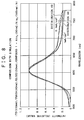
- the EL spectrum of the sample No. Device (3-6) is shown in FIG. 5.
- the EL spectrum exhibits the peak value at a wavelength near 650 nm, which indicates the compound 2, and a small peak value at a wavelength near 520 nm, which indicates Alq 3 .
- the EL spectrum of the sample No. Device (3-3) shown in FIG. 6 it is apparent that light emission occurs nearly in the whole range of the light emission layer and that no light emission of Alq 3 occur.
- a device was produced with a film thickness condition that a light interference effect between light emerged from a light emission interface and light reflected from an aluminum electrode 37 weakens light outputted from the device.
- An ITO electrode 36 (thickness: 119 nm), a TNATA (4,4',4"-tris (2-naphthylphenylamino)triphenylamine) layer 32a (thickness: 40 nm), an EL022 (triphenylamine tetramer) layer 32b (thickness: 50 nm), an Alq 3 layer 33 mixed with 40% of the above-described styryl compound 1 (thickness: 50 nm), and an Alq 3 layer 34 (thickness: 165 nm) were sequentially stacked, and the aluminum electrode 37 was formed thereon. A relationship between an actually measured emission spectrum of this device and an emission spectrum estimated from a light emission distribution in the light emission layer of the device was examined.
- a light emission distribution 49 in the light emission layer corresponds to an emission spectrum of the device operated at a current density of 0.1 mA/cm 2
- a light emission distribution 46 in the light emission layer corresponds to an emission spectrum of the device operated at a current density of 1mA/cm 2 .
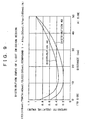
- the light emission distribution in the light emission layer used for calculation is shown in FIG. 9.
- the intensity can be obtained. Further, by integrating the intensity with a luminous intensity distribution in each depth direction and calculating the integrated intensity for each wavelength, a spectrum of the light ray emerged to the outside can be obtained.
- the emission spectrum exhibits that a distribution of a light emission region having a large luminous intensity occurs at both of the interface between the hole transport layer and the light emission layer and the interface between the electron transport layer and the light emission layer.
- the light emission distribution on the hole transport layer side increases with the increased current density.
- a light emission region is formed by a mixed layer made from a luminous material exhibiting electroluminescence when a voltage is applied thereto and having a charge transport characteristic and a charge injection accelerating material capable of accelerating injection of charges in the luminous material, and the light emission region exists not only at an interface with an adjacent layer or its vicinity but also over a specific thickness region in the layer thickness direction. Accordingly, a region in which light is emitted is not limited to the above-described interface or its vicinity but is spread in a wide range of the light emission layer. As a result, it is possible to significantly improve the service life of the device. Further, it is possible to prevent the hue of light from being varied depending on the concentration of the luminous material contained in the light emission layer and on an operational condition such as an applied voltage, and hence to stabilize the performance of the device.
Landscapes
- Physics & Mathematics (AREA)
- Optics & Photonics (AREA)
- Electroluminescent Light Sources (AREA)
Applications Claiming Priority (5)
| Application Number | Priority Date | Filing Date | Title |
|---|---|---|---|
| JP2002111659 | 2002-04-15 | ||
| JP2002111659 | 2002-04-15 | ||
| JP2002138212A JP2004006066A (ja) | 2002-04-15 | 2002-05-14 | 有機電界発光素子及び発光装置 |
| JP2002138212 | 2002-05-14 | ||
| PCT/JP2002/005366 WO2003088721A1 (en) | 2002-04-15 | 2002-05-31 | Organic field emission device and emission device |
Publications (2)
| Publication Number | Publication Date |
|---|---|
| EP1511363A1 true EP1511363A1 (de) | 2005-03-02 |
| EP1511363A4 EP1511363A4 (de) | 2010-08-25 |
Family
ID=29253553
Family Applications (1)
| Application Number | Title | Priority Date | Filing Date |
|---|---|---|---|
| EP02730838A Withdrawn EP1511363A4 (de) | 2002-04-15 | 2002-05-31 | Organische feldemissionsvorrichtung und feldemissionsvorrichtung |
Country Status (7)
| Country | Link |
|---|---|
| US (1) | US20050064232A1 (de) |
| EP (1) | EP1511363A4 (de) |
| JP (1) | JP2004006066A (de) |
| KR (1) | KR20040044066A (de) |
| CN (1) | CN100442568C (de) |
| TW (1) | TWI293011B (de) |
| WO (1) | WO2003088721A1 (de) |
Families Citing this family (12)
| Publication number | Priority date | Publication date | Assignee | Title |
|---|---|---|---|---|
| JP4001118B2 (ja) * | 2003-03-24 | 2007-10-31 | ソニー株式会社 | 有機電界発光素子及びアミノモノスチリルナフタレン化合物 |
| EP2924094B1 (de) * | 2003-06-02 | 2017-04-05 | UDC Ireland Limited | Organische elektrolumineszenzvorrichtungen und metallkomplexverbindungen |
| KR100981015B1 (ko) * | 2004-03-25 | 2010-09-07 | 사천홍시현시기건유한공사 | 유기 전계 발광 소자의 제조 방법 |
| CN100455151C (zh) * | 2005-08-30 | 2009-01-21 | 铼宝科技股份有限公司 | 有机电激发光元件及其制造方法 |
| US20070215889A1 (en) * | 2006-03-20 | 2007-09-20 | Semiconductor Energy Laboratory Co., Ltd. | Aromatic amine compound, and light-emitting element, light-emitting device, and electronic appliance using the aromatic amine compound |
| JP5207645B2 (ja) * | 2006-03-29 | 2013-06-12 | キヤノン株式会社 | 多色有機発光装置 |
| CN101919082B (zh) * | 2007-12-28 | 2012-05-30 | 夏普株式会社 | 有机电致发光元件 |
| KR101320107B1 (ko) * | 2007-12-31 | 2013-10-18 | 엘지디스플레이 주식회사 | 유기전계발광표시장치 |
| US8242489B2 (en) * | 2009-12-17 | 2012-08-14 | Global Oled Technology, Llc. | OLED with high efficiency blue light-emitting layer |
| JP6094480B2 (ja) * | 2011-06-15 | 2017-03-15 | コニカミノルタ株式会社 | 有機エレクトロルミネッセンス素子、照明装置、表示装置及び有機エレクトロルミネッセンス素子の製造方法 |
| KR101963226B1 (ko) * | 2012-02-29 | 2019-04-01 | 삼성전자주식회사 | 트랜지스터와 그 제조방법 및 트랜지스터를 포함하는 전자소자 |
| JP2018022862A (ja) * | 2016-07-20 | 2018-02-08 | 株式会社Joled | 有機電界発光素子、有機電界発光装置および電子機器 |
Family Cites Families (12)
| Publication number | Priority date | Publication date | Assignee | Title |
|---|---|---|---|---|
| JP2814435B2 (ja) * | 1987-03-02 | 1998-10-22 | イーストマン・コダック・カンパニー | 改良薄膜発光帯をもつ電場発光デバイス |
| JP2869446B2 (ja) * | 1989-01-13 | 1999-03-10 | 株式会社リコー | 電界発光素子 |
| US5085946A (en) * | 1989-01-13 | 1992-02-04 | Ricoh Company, Ltd. | Electroluminescence device |
| JP2879080B2 (ja) * | 1989-03-23 | 1999-04-05 | 株式会社リコー | 電界発光素子 |
| JP3712760B2 (ja) * | 1995-05-17 | 2005-11-02 | Tdk株式会社 | 有機el素子 |
| JPH10270166A (ja) * | 1997-03-27 | 1998-10-09 | Tatsuo Mori | 電界発光素子 |
| DE19803889A1 (de) * | 1998-01-31 | 1999-08-05 | Bosch Gmbh Robert | Elektrolumineszierende Anordnung unter Verwendung von dotierten Blendsystemen |
| JP3852517B2 (ja) * | 1998-05-18 | 2006-11-29 | ソニー株式会社 | 有機電界発光素子 |
| JP3555736B2 (ja) | 1998-06-26 | 2004-08-18 | ソニー株式会社 | 有機電界発光素子 |
| JP2001052870A (ja) * | 1999-06-03 | 2001-02-23 | Tdk Corp | 有機el素子 |
| JP2001291591A (ja) * | 2000-04-07 | 2001-10-19 | Sony Corp | 有機電界発光素子及び発光装置 |
| JP4273191B2 (ja) * | 2001-03-01 | 2009-06-03 | 三星モバイルディスプレイ株式會社 | 有機発光デバイス |
-
2002
- 2002-05-14 JP JP2002138212A patent/JP2004006066A/ja active Pending
- 2002-05-23 TW TW091110879A patent/TWI293011B/zh not_active IP Right Cessation
- 2002-05-31 EP EP02730838A patent/EP1511363A4/de not_active Withdrawn
- 2002-05-31 KR KR1020027012973A patent/KR20040044066A/ko not_active Ceased
- 2002-05-31 US US10/240,328 patent/US20050064232A1/en not_active Abandoned
- 2002-05-31 WO PCT/JP2002/005366 patent/WO2003088721A1/ja not_active Ceased
- 2002-09-30 CN CNB021545545A patent/CN100442568C/zh not_active Expired - Fee Related
Also Published As
| Publication number | Publication date |
|---|---|
| JP2004006066A (ja) | 2004-01-08 |
| TWI293011B (de) | 2008-01-21 |
| EP1511363A4 (de) | 2010-08-25 |
| WO2003088721A1 (en) | 2003-10-23 |
| CN100442568C (zh) | 2008-12-10 |
| CN1452439A (zh) | 2003-10-29 |
| KR20040044066A (ko) | 2004-05-27 |
| US20050064232A1 (en) | 2005-03-24 |
Similar Documents
| Publication | Publication Date | Title |
|---|---|---|
| US7510783B2 (en) | Organic light-emitting element and display device | |
| US6582838B2 (en) | Red-emitting organic light emitting devices (OLED's) | |
| JP4181795B2 (ja) | エレクトロルミネッセンス素子 | |
| EP1516902A1 (de) | Organisches elektrolumineszenzelement und es enthaltende elektrolumineszierende vorrichtung oder anzeige | |
| US7255935B2 (en) | Organic electroluminescent element and luminescent apparatus employing the same | |
| KR20010049923A (ko) | 유기 전계 발광 소자 | |
| JP2003323155A (ja) | 電界発光素子の駆動方法 | |
| EP1511363A1 (de) | Organische feldemissionsvorrichtung und feldemissionsvorrichtung | |
| JP3143362B2 (ja) | 有機エレクトロルミネッセンス素子 | |
| JP2002313579A (ja) | 有機電界発光素子及び表示装置 | |
| KR100572654B1 (ko) | 유기 전계발광 소자 | |
| KR100547055B1 (ko) | 유기 전계발광 소자 | |
| US20050067950A1 (en) | Organic electroluminescent device | |
| JP3143350B2 (ja) | 有機エレクトロルミネッセンス素子 | |
| KR100581639B1 (ko) | 유기 전계발광 소자 | |
| US20040219390A1 (en) | Benzoxazinone and quinazolinone derivatives | |
| KR100581640B1 (ko) | 유기 전계발광 소자 | |
| WO2003091357A1 (en) | Organic electroluminescent element |
Legal Events
| Date | Code | Title | Description |
|---|---|---|---|
| PUAI | Public reference made under article 153(3) epc to a published international application that has entered the european phase |
Free format text: ORIGINAL CODE: 0009012 |
|
| 17P | Request for examination filed |
Effective date: 20040305 |
|
| AK | Designated contracting states |
Kind code of ref document: A1 Designated state(s): AT BE CH CY DE DK ES FI FR GB GR IE IT LI LU MC NL PT SE TR |
|
| A4 | Supplementary search report drawn up and despatched |
Effective date: 20100728 |
|
| 17Q | First examination report despatched |
Effective date: 20110224 |
|
| GRAP | Despatch of communication of intention to grant a patent |
Free format text: ORIGINAL CODE: EPIDOSNIGR1 |
|
| RIC1 | Information provided on ipc code assigned before grant |
Ipc: H01L 51/50 20060101ALI20110930BHEP Ipc: H05B 33/14 20060101AFI20110930BHEP |
|
| RIN1 | Information on inventor provided before grant (corrected) |
Inventor name: UEDA, NAOYUKI Inventor name: TAMURA, SHINICHIRO Inventor name: YAMADA, JIRO Inventor name: ICHIMURA, MARI Inventor name: ISHIBASHI, TADASHI |
|
| STAA | Information on the status of an ep patent application or granted ep patent |
Free format text: STATUS: THE APPLICATION IS DEEMED TO BE WITHDRAWN |
|
| 18D | Application deemed to be withdrawn |
Effective date: 20120307 |